


查询BFG520X供应商
DISCRETE SEMICONDUCTORS
DATA SH EET
BFG520; BFG520/X; BFG520/XR
NPN 9 GHz wideband transistor
Product specification
File under Discrete Semiconductors, SC14
September 1995

Philips Semiconductors Product specification
NPN 9 GHz wideband transistor BFG520; BFG520/X; BFG520/XR
FEATURES
• High power gain
• Low noise figure
• High transition frequency
• Gold metallization ensures
excellent reliability.
DESCRIPTION
NPN silicon planar epitaxial
transistors, intended for applications
in the RF frontend in the GHz range,
such as analog and digital cellular
telephones, cordless telephones
(CT1, CT2, DECT, etc.), radar
detectors, pagers and satellite TV
tuners (SATV) and repeater
amplifiers in fibre-optic systems.
The transistors are encapsulated in
4-pin, dual-emitter plastic SOT143
and SOT143R envelopes.
PINNING
PIN DESCRIPTION
BFG520 (Fig.1) Code: N36
1 collector
2 base
3 emitter
4 emitter
BFG520/X (Fig.1) Code: N42
1 collector
2 emitter
3 base
4 emitter
BFG520/XR (Fig.2) Code: N48
1 collector
2 emitter
3 base
4 emitter
page
12
Top view
Fig.1 SOT143B.
handbook, 2 columns
Top view
Fig.2 SOT143R.
34
MSB014
43
12
MSB035
QUICK REFERENCE DATA
SYMBOL PARAMETER CONDITIONS MIN. TYP. MAX. UNIT
V
CBO
V
CEO
I
c
P
tot
h
FE
C
re
f
T
G
UM
2
S
21
F noise figure Γ
collector-base voltage open emitter −−20 V
collector-emitter voltage open base −−15 V
DC collector current −−70 mA
total power dissipation up to Ts=88°C; note 1 −−300 mW
DC current gain IC= 20 mA; VCE= 6 V; Tj=25°C 60 120 250
feedback capacitance IC = 0; VCB = 6 V; f = 1 MHz − 0.3 − pF
transition frequency IC= 20 mA; VCE= 6 V; f = 1 GHz;
=25°C
T
amb
maximum unilateral
power gain
IC= 20 mA; VCE= 6 V; f = 900 MHz;
T
=25°C
amb
I
= 20 mA; VCE= 6 V; f = 2 GHz;
C
T
=25°C
amb
insertion power gain IC= 20 mA; VCE= 6 V; f = 900 MHz;
T
=25°C
amb
= Γ
s
f = 900 MHz; T
Γ
s
f = 900 MHz; T
Γ
s
f = 2 GHz; T
; Ic= 5 mA; VCE=6V;
opt
=25°C
amb
= Γ
; IC= 20 mA; VCE=6 V;
opt
=25°C
amb
= Γ
; IC= 5 mA; VCE= 8 V;
opt
=25°C
amb
− 9 − GHz
− 19 − dB
− 13 − dB
17 18 − dB
− 1.1 1.6 dB
− 1.6 2.1 dB
− 1.9 − dB
September 1995 2

Philips Semiconductors Product specification
NPN 9 GHz wideband transistor BFG520; BFG520/X; BFG520/XR
LIMITING VALUES
In accordance with the Absolute Maximum System (IEC 134).
SYMBOL PARAMETER CONDITIONS MIN. MAX. UNIT
V
CBO
V
CEO
V
EBO
I
C
P
tot
T
stg
T
j
THERMAL RESISTANCE
SYMBOL PARAMETER CONDITIONS THERMAL RESISTANCE
R
th j-s
collector-base voltage open emitter − 20 V
collector-emitter voltage open base − 15 V
emitter-base voltage open collector − 2.5 V
DC collector current − 70 mA
total power dissipation up to Ts = 88 °C; note 1 − 300 mW
storage temperature −65 150 °C
junction temperature − 175 °C
thermal resistance from junction to
up to Ts=88°C; note 1 290 K/W
soldering point
Note
1. T
is the temperature at the soldering point of the collector tab.
s
September 1995 3

Philips Semiconductors Product specification
NPN 9 GHz wideband transistor BFG520; BFG520/X; BFG520/XR
CHARACTERISTICS
T
= 25 °C unless otherwise specified.
j
SYMBOL PARAMETER CONDITIONS MIN. TYP. MAX. UNIT
I
CBO
h
FE
C
e
C
c
C
re
f
T
G
UM
S
21
F noise figure Γ
P
L1
ITO third order intercept point note 2 − 26 − dBm
V
o
d
2
collector cut-off current IE = 0; VCB = 6 V −− 50 nA
DC current gain IC= 20 mA; VCE= 6 V 60 120 250
emitter capacitance IC=ic=0;VEB= 0.5 V; f = 1 MHz − 1 − pF
collector capacitance IE=ie=0;VCB= 6 V; f = 1 MHz − 0.6 − pF
feedback capacitance IC=0;VCB= 6 V; f = 1 MHz − 0.3 − pF
transition frequency IC = 20 mA; VCE = 6 V; f = 1 GHz;
T
=25°C
amb
maximum unilateral
power gain (note 1)
2
insertion power gain IC= 20 mA; VCE= 6 V; f = 900 MHz;
output power at 1 dB gain
compression
IC= 20 mA; VCE= 6 V; f = 900 MHz;
T
= 25 °C
amb
I
= 20 mA; VCE= 6 V; f = 2 GHz;
C
T
= 25 °C
amb
T
= 25 °C
amb
= Γ
s
f = 900 MHz; T
= Γ
Γ
s
f = 900 MHz; T
Γ
= Γ
s
f = 2 GHz; T
= 5 mA; VCE=6V;
opt;IC
=25°C
amb
; IC= 20 mA; VCE=6 V;
opt
=25°C
amb
= 5 mA; VCE=6 V;
opt;IC
=25°C
amb
IC= 20 mA; VCE= 6 V; RL=50Ω;
f = 900 MHz; T
amb
=25°C
− 9 − GHz
− 19 − dB
− 13 − dB
17 18 − dB
− 1.1 1.6 dB
− 1.6 2.1 dB
− 1.9 − dB
− 17 − dBm
output voltage note 3 − 275 − mV
second order intermodulation
distortion
IC= 20 mA; VCE= 6 V; Vo= 75 mV;
T
amb
=25°C; f
(p+q)
= 810 MHz
−−50 − dB
Notes
1. G
2. I
is the maximum unilateral power gain, assuming S12is zero and
UM
G
UM
= 20 mA; VCE= 6 V; RL=50Ω; f = 900 MHz; T
C
--------------------------------------------------------------
10 log
1S
–
2
S
21
2
1S
–
11
22
dB.=
2
=25°C;
amb
fp= 900 MHz; fq= 902 MHz;
measured at f
= 898 MHz and f
(2p−q)
(2q−p)
= 904 MHz.
3. dim= −60 dB (DIN 45004B);
Vp=Vo;Vq=Vo−6 dB; Vr=Vo−6 dB;
fp= 795.25 MHz; fq= 803.25 MHz; fr= 805.25 MHz;
measured at f
= 793.25 MHz
(p+q−r)
September 1995 4
Philips Semiconductors Product specification
NPN 9 GHz wideband transistor BFG520; BFG520/X; BFG520/XR
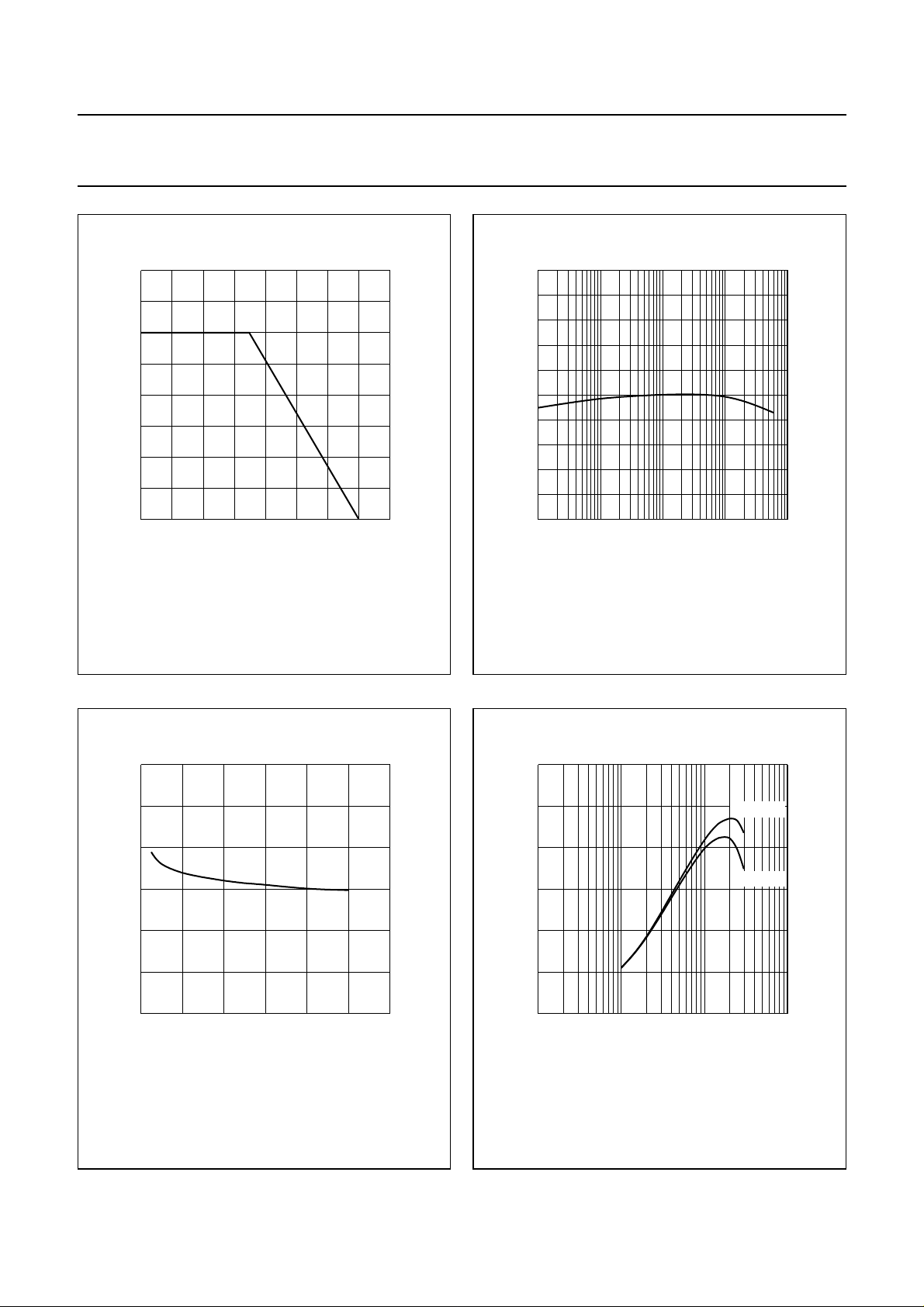
400
handbook, halfpage
P
tot
(mW)
300
200
100
0
0 50 100 200
150
Ts (oC)
Fig.3 Power derating curve.
MRA670-1
250
handbook, halfpage
h
FE
200
150
100
50
0
−2
10
VCE= 6 V; Tj=25°C.
−1
10
11010
MRA671
IC (mA)
Fig.4 DC current gain as a function of collector
current.
2
0.6
handbook, halfpage
C
re
(pF)
0.4
0.2
0
0
IC= 0; f = 1 MHz.
4812
VCB (V)
Fig.5 Feedback capacitance as a function of
collector-base voltage.
MRA672
12
handbook, halfpage
f
T
(GHz)
8
4
0
−1
10
f = 1 GHz; T
amb
11010
=25°C.
V
V
IC (mA)
Fig.6 Transition frequency as a function of
collector current.
CE
CE
MRA673
= 6 V
= 3 V
2
September 1995 5
Philips Semiconductors Product specification
NPN 9 GHz wideband transistor BFG520; BFG520/X; BFG520/XR
In Figs 7 to 10, GUM= maximum unilateral power gain;
MSG = maximum stable gain; G
gain.
= maximum available
max
25
handbook, halfpage
gain
(dB)
VCE= 6 V; f = 900 MHz; T
MSG
20
15
10
5
0
010
=25°C.
amb
20 30
Fig.7 Gain as a function of collector current.
MRA674
G
max
G
UM
I
(mA)
C
25
handbook, halfpage
gain
(dB)
20
15
MSG
10
5
0
010
VCE= 6 V; f = 2 GHz; T
amb
=25°C.
G
max
G
UM
20 30
Fig.8 Gain as a function of collector current.
MRA675
I
(mA)
C
G
max
f (MHz)
MRA676
4
10
50
handbook, halfpage
gain
(dB)
IC= 5 mA; VCE= 6 V; T
G
40
MSG
30
20
10
0
10
UM
10
amb
2
=25°C.
3
10
Fig.9 Gain as a function of frequency.
September 1995 6
50
handbook, halfpage
gain
(dB)
40
30
20
10
0
10
IC= 20 mA; VCE= 6 V; T
Fig.10 Gain as a function of frequency.
10
amb
G
UM
MSG
2
=25°C.
MRA677
G
max
3
10
f (MHz)
4
10

Philips Semiconductors Product specification
NPN 9 GHz wideband transistor BFG520; BFG520/X; BFG520/XR
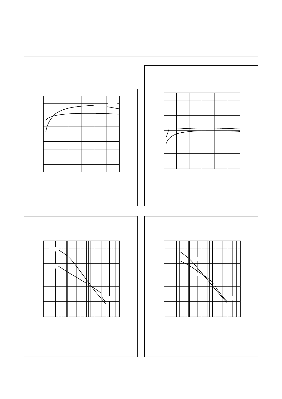
40
MEA975
IC (mA)
−20
handbook, halfpage
d
im
(dB)
−30
−40
−50
−60
−70
050
10 20 30
Fig.11 Intermodulation distortion as a function of
collector current.
40
MEA974
IC (mA)
−20
handbook, halfpage
d
2
(dB)
−30
−40
−50
−60
−70
050
10 20 30
Fig.12 Second order intermodulation distortion as
a function of collector current.
handbook, halfpage
5
F
min
(dB)
4
3
2000 MHz
2
1000 MHz
1
900 MHz
500 MHz
0
1
VCE= 6 V; T
amb
=25°C.
f = 900 MHz
1000 MHz
G
ass
2000 MHz
F
min
10
IC (mA)
Fig.13 Minimum noise figure and associated
available gain as functions of collector
current.
MRA682
20
G
ass
(dB)
15
10
5
0
−5
2
10
handbook, halfpage
5
F
min
(dB)
4
3
2
20 mA
1
5 mA
0
2
10
VCE= 6 V; T
amb
IC = 5 mA
=25°C.
20 mA
G
ass
F
min
3
10
f (MHz)
MRA683
20
G
ass
(dB)
15
10
5
0
−5
4
10
Fig.14 Minimum noise figure and associated
available gain as functions of frequency.
September 1995 7

Philips Semiconductors Product specification
NPN 9 GHz wideband transistor BFG520; BFG520/X; BFG520/XR
handbook, full pagewidth
IC= 5 mA; VCE= 6 V;
f =900 MHz; Z
o
=50Ω.
pot. unst.
region
180°
stability
circle
135°
0
0.2
−135°
0.5
0.2
0.2 0.5 1 2 5
0.5
F = 2 dB
F = 3 dB
90°
1
F
min
F = 1.5 dB
1
−90°
Fig.15 Noise circle figure.
= 1. 1 dB
Γ
OPT
1.0
45°
2
5
5
2
−45°
MRA684
0.8
0.6
0.4
0.2
0°
0
1.0
handbook, full pagewidth
IC= 5 mA; VCE= 6 V;
f =2 GHz; Z
=50Ω.
o
180°
G
max
135°
= 13 dB
Γ
0
0.2
−135°
0.5
0.2
0.2 0.5 1
MS
G = 12 dB
G = 11 dB
G = 10 dB
0.5
90°
1
F = 3 dB
F = 2.5 dB
F = 2 dB
Γ
OPT
F
= 1. 9 dB
min
2 5
1
−90°
Fig.16 Noise circle figure.
1.0
45°
2
5
5
2
−45°
MRA685
0.8
0.6
0.4
0.2
0°
0
1.0
September 1995 8

Philips Semiconductors Product specification
NPN 9 GHz wideband transistor BFG520; BFG520/X; BFG520/XR
handbook, full pagewidth
IC= 20 mA; VCE= 6 V.
Zo=50Ω.
90°
1
180°
135°
0
0.2
−135°
0.5
3 GHz
0.2
0.2 0.5 1 2 5
0.5
1
−90°
40 MHz
45°
2
2
−45°
Fig.17 Common emitter input reflection coefficient (S11).
5
5
MRA678
1.0
0.8
0.6
0.4
0.2
0°
0
1.0
handbook, full pagewidth
IC= 20 mA; VCE= 6 V.
90°
135°
45°
40 MHz
−90°
3 GHz
0°
−45°
MRA679
180°
50 40 30 20 10
−135°
Fig.18 Common emitter forward transmission coefficient (S21).
September 1995 9

Philips Semiconductors Product specification
NPN 9 GHz wideband transistor BFG520; BFG520/X; BFG520/XR
handbook, full pagewidth
IC= 20 mA; VCE= 6 V.
90°
135°
45°
3 GHz
180°
0.25 0.20 0.15 0.10 0.05
−135°
40 MHz
−45°
−90°
0°
MRA680
Fig.19 Common emitter reverse transmission coefficient (S12).
handbook, full pagewidth
IC= 20 mA; VCE= 6 V.
Zo=50Ω.
90°
1
180°
135°
0
0.5
0.2
0.2 0.5 1 2 5
45°
2
5
40 MHz
0.2
−135°
0.5
3 GHz
2
1
−90°
5
−45°
Fig.20 Common emitter output reflection coefficient (S22).
MRA681
1.0
0.8
0.6
0.4
0.2
0°
0
1.0
September 1995 10
Philips Semiconductors Product specification
NPN 9 GHz wideband transistor BFG520; BFG520/X; BFG520/XR
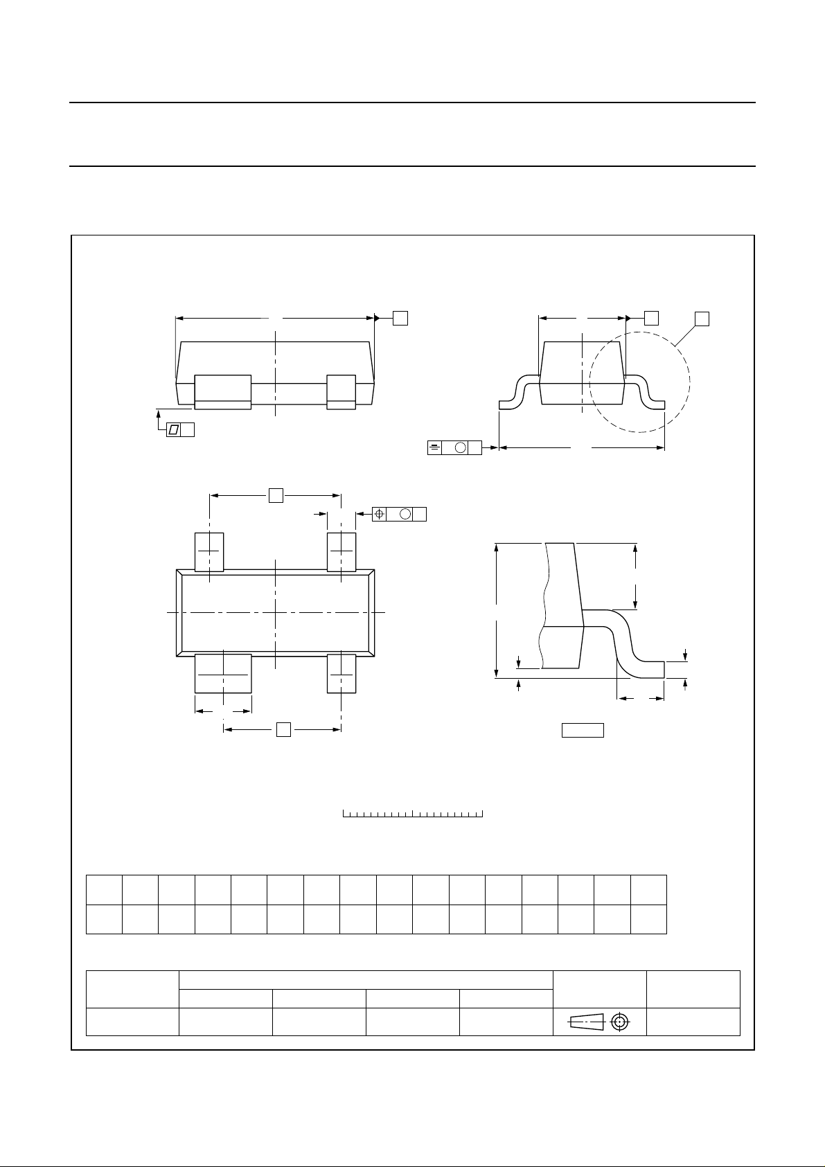
PACKAGE OUTLINES
Plastic surface mounted package; 4 leads SOT143B
D
y
e
b
p
B
w M
E
v M
A
B
H
E
A
X
34
Q
A
A
1
21
b
1
e
1
detail X
L
c
p
0 1 2 mm
scale
DIMENSIONS (mm are the original dimensions)
A
UNIT
mm
VERSION
A
1.1
0.9
OUTLINE
SOT143B
max
0.1
1
b
c
b
0.48
0.38
1
p
0.88
0.15
0.78
0.09
IEC JEDEC EIAJ
D
3.0
2.8
REFERENCES
1.4
1.2
E
e
1.9
September 1995 11
e
1.7
H
L
E
1
2.5
2.1
0.45
0.15
p
0.55
0.45
EUROPEAN
PROJECTION
ywvQ
0.1 0.10.2
ISSUE DATE
97-02-28

Philips Semiconductors Product specification
NPN 9 GHz wideband transistor BFG520; BFG520/X; BFG520/XR
Plastic surface mounted package; reverse pinning; 4 leads SOT143R
D
y
e
b
p
B
w M
E
v M
A
B
H
E
A
X
43
Q
A
A
1
c
12
L
b
1
e
1
detail X
p
0 1 2 mm
scale
DIMENSIONS (mm are the original dimensions)
A
UNIT
mm
VERSION
A
1.1
0.9
OUTLINE
SOT143R
max
0.1
1
b
c
b
0.48
0.38
1
p
0.88
0.15
0.78
0.09
IEC JEDEC EIAJ
D
3.0
2.8
REFERENCES
1.4
1.2
E
e
1.9
September 1995 12
e
1.7
H
L
E
1
2.5
2.1
0.55
0.25
p
0.45
0.25
EUROPEAN
PROJECTION
ywvQ
0.1 0.10.2
ISSUE DATE
97-03-10

Philips Semiconductors Product specification
NPN 9 GHz wideband transistor BFG520; BFG520/X; BFG520/XR
DEFINITIONS
Data Sheet Status
Objective specification This data sheet contains target or goal specifications for product development.
Preliminary specification This data sheet contains preliminary data; supplementary data may be published later.
Product specification This data sheet contains final product specifications.
Limiting values
Limiting values given are in accordance with the Absolute Maximum Rating System (IEC 134). Stress above one or
more of the limiting values may cause permanent damage to the device. These are stress ratings only and operation
of the device at these or at any other conditions above those given in the Characteristics sections of the specification
is not implied. Exposure to limiting values for extended periods may affect device reliability.
Application information
Where application information is given, it is advisory and does not form part of the specification.
LIFE SUPPORT APPLICATIONS
These products are not designed for use in life support appliances, devices, or systems where malfunction of these
products can reasonably be expected to result in personal injury. Philips customers using or selling these products for
use in such applications do so at their own risk and agree to fully indemnify Philips for any damages resulting from such
improper use or sale.
September 1995 13
 Loading...