

Philips VR540/39, VR740/02, VR540/58, VR740/16, VR740/58 Service Manual
...
Video Cassette Recorder
VR540
/39
VR740
/58
Service
Service
Service
VR540
VR740
VR740
VR740
/58
/02
/07
/16
VR742
VR742
VR742
/16
/39
/58
Service Manual
Contents
Chapter
Schematic Diagrams and CBA's
Sec. 1:
Exploded Views
Mechanical and Electrical Parts Lists
Survey of versions:
/02 PAL B/G
/07 PAL I, Ireland
/16 PAL B/G, Spain
/39 SECAM L,L' & PAL B/G
/58 PAL/SECAM B/G, D/K
For technical data reference is made to the Service Manual of VR540/02/07/16
3103 785 22160. The present manual states only the differences.
Safety regulations require that the set be restored to its original
condition and that parts which are identical with those specified
be used.
Published by BK 2003 Video Service Department Printed in Japan c
Copyright reserved Subject to modification GB 3103 785 22170

OPERATING CONTROLS AND FUNCTIONS
1 2 3
4 5 6
7 8 9
P
0
P
P
STILL
STOP
MENU
REW FWD
PLAYSTATUS/EXIT CLEAR
VCR TV
REC STANDBY/ON
PROGVOL
INDEXMUTE SLOW SYSTEM
AUDIO
y
[ VR540/ (39,58)]
The remote control
Buttons for VCR feature only
VCR
To operate the VCR with the remote control.
CLEAR
(TIMER).
press repeatedly to start a One-Touch Recording.
During normal or slow motion playback, press to adjust the
tracking.
INDEX
next
SLOW
AUDIO
SYSTEM
MENU
FWD
forward the tape at high speed. During playback, press to fast
forward the tape while the picture stay on the screen. To store or
confirm entry in the menu.
REW
the tape at high speed. During playback, press to rewind the
tape while the picture stay on the screen.To return the cursor in
the menu.
PLAY
STOP
VCR.
To delete last entry/Clear programmed recording
REC
To record the TV channel selected at this moment or
STILL
To stop the tape and slow a still picture.
+
PROG P–PROG P
In combination with
To select the programme number.
:to search for previous or
0 /1
recording on the cassette.
To view the picture in slow motion.
To change stereo sound and 2nd language.
To change the video (colour) system.
To call up main menu of VCR.
When tape playback is stopped, press to fast
-
When tape playback is stoped, press to rewind
-
K
To play a tape, select an item in the menu of VCR.
B-
C- L
To stop the tape, select an item in the menu of
Buttons with TV feature
TV
To call up additional TV functions.
y
STANDBY/ON
To switch VCR or Philips TV on or off, interrupt menu
function.
STATUS/EXIT
To access or remove the VCR’s on-screen status display.
To exit on-screen menus. Or, to access or remove a status display or menu
of Philips TV.
0..9
Press to select channels at VCR or Philips TV.
MUTE
To eliminate the TV’s sound. Press again to restore the volume.
VOL 5
VCR
–
To adjust the TV’s volume.
+
VOL
Press before pressing a VCR-feature key.
You can use this remote control to operate some func-
tions of Philips TVs. Press before pressing a TV-
TV
feature key.
1-5-3 HE473IB
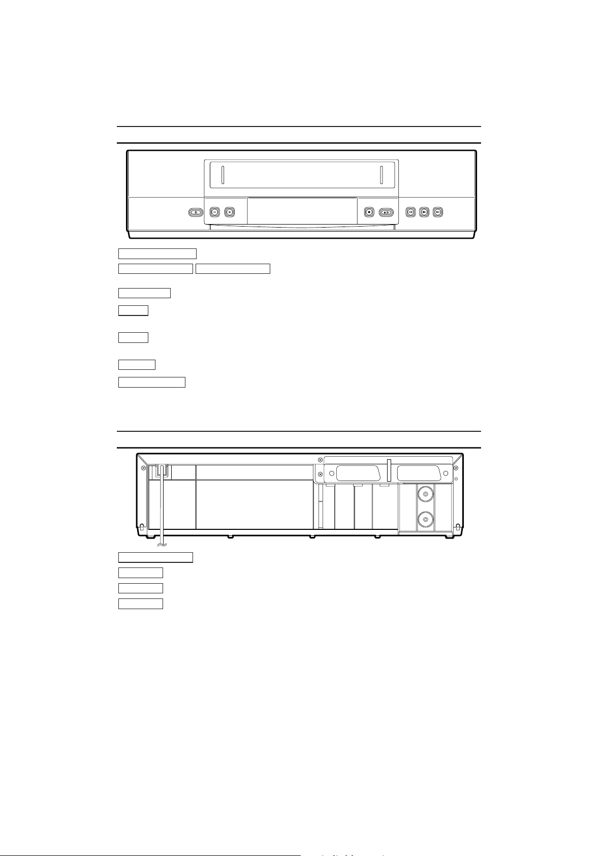
Front of the device
RF OUT
AV2 (DECODER) AV1 (TV)
AERIAL
FWDPLAYREWSTOP/EJECTRECORDPROGRAMMESTANDBY/ON
STANDBY/ON
motion playback, press to adjust the tracking.
RECORD
When tape playback is stopped, press to fast forward the tape at hight speed. During
FWD
playback, press to fast forward the tape while the picture stay on the screen.
When tape playback is stoped, press to rewind the tape at hight speed. During playback,
REW
press to rewind the tape while the picture stay on the screen.
PLAY
To play a tape.
STOP/EJECT
To switch off or on, interrupt a function.
PROGRAMME-PROGRAMME+
To record the TV channel selected at this moments.
To stop the tape and eject the cassette.
To select the programme number. During normal or slow
Back of the set
AV2(DECODER)
AV1(TV)
AERIAL
RF OUT
To connect the TV set(programme number).
To connect the aerial cable.
To connect the TV set.
To connect a satellite receiver, decoder, video recorder,etc.
1-5-4 HE473IB
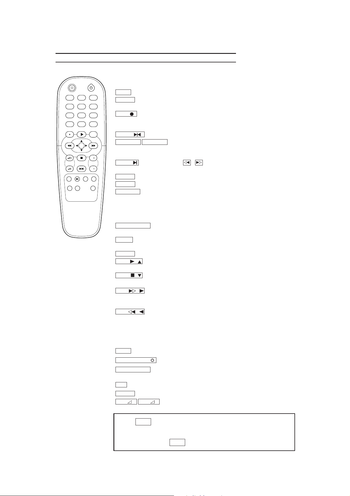
[ VR740/ (02, 07, 16, 58), VR742/ (16, 39, 58) ]
The remote control
REC STANDBY/ON
1 2 3
4 5 6
7 8 9
VCR TV
0
PLAYSTATUS/EXIT CLEAR
REW FWD
MENU
STOP
PROGVOL
STILL
INDEXMUTE SLOW SYSTEM
TURBO
SV / V+ AUDIO
TIMER
Buttons for VCR feature only
VCR
To operate the VCR with the remote control.
CLEAR
recording (TIMER).
moment or press repeatedly to start a One-Touch
Recording.
STILL
number. During normal or slow motion playback, press
P
P
to adjust the tracking.
INDEX
P
previous or next recording on the cassette.
SLOW
AUDIO
SYSTEM
[ VR740/ (02, 07, 16), VR742/ (16) ]
[ VR740/ (58), VR742/ (39, 58) ]
TURBO TIMER
function TURBO TIMER.
SV/V
SHOWVIEW system.
PLAY
of VCR.
STOP
menu of VCR
FWD
speed. During playback, press to fast forward the tape while the picture stay on the
screen. To store or confirm entry in the menu.
REW
speed. During playback, press to rewind the tape while the picture stay on the
screen.To return the cursor in the menu.
To delete last entry/Clear programmed
REC
To record the TV channel selected at this
To stop the tape and slow a still picture.
+
PROG P–PROG P
To select the programme
In combination with / :to search for
To view the picture in slow motion.
To change stereo sound and 2nd language.
Doesn’t
work in these
models.
To change the video (colour) system.
To programme a recording with the
+
To make a TIMER programming with
To call up main menu of VCR.
MENU
To play a tape, select an item in the menu
-
To stop the tape, select an item in the
-
When tape playback is stopped, press to fast forward the tape at high
-
When tape playback is stoped, press to rewind the tape at high
-
Buttons with TV feature
TV
To call up additional TV functions.
STANDBY/ON
STATUS/EXIT
on-screen menus. Or, to access or remove a status display or menu of Philips TV.
0..9
Press to select channels at VCR or Philips TV.
MUTE
To mute the TV’s sound. Press again to restore the volume.
+
VOL
Press before pressing a VCR-feature key.
VOL
VCR
You can use this remote control to operate some functions of
Philips TVs. Press before pressing a TV-feature key.
To switch VCR or Philips TV on or off, interrupt menu function.
To access or remove the VCR’s on-screen status display. To exit
–
To adjust the TV’s volume.
TV
1-5-5 HE473IB
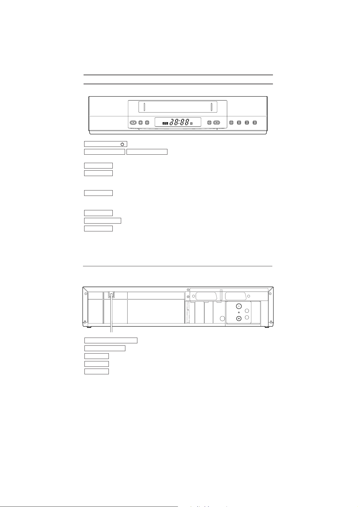
Front of the device
STANDBY/ON
STANDBY/ON
PROGRAMME
PWR. REC
RECORD
To switch off or on, interrupt a function.
PROGRAMME-PROGRAMME+
To select the programme number. During
STOP/EJECT
FWDPLAYREWSTILL
normal or slow motion playback, press to adjust the tracking.
RECORD
To record the TV channel selected at this moments.
FWD
When tape playback is stopped, press to fast forward the tape at high speed.
During playback, press to fast forward the tape while the picture stay on the screen.
REW
When tape playback is stoped, press to rewind the tape at hight speed. During
playback, press to rewind the tape while the picture stay on the screen.
PLAY
STOP/EJECT
STILL
To play a tape.
To stop the tape and eject the cassette.
o stop the tape and slow a still picture.
T
Back of the set
AV 2 (DECODER) AV 1 (TV)
AUDIO OUTPUT L
AV2(DECODER)
AV1(TV)
AERIAL
RF OUT
To connect the TV set.
To connect the aerial cable.
To connect the TV set.
AUDIO
OUTPUT
AERIAL
L
RF OU T
R
To connect a HIFI-set.
R
To connect a satellite receiver, decoder, video recorder,etc.
1-5-6 HE473IB
SIGNAL NAME ABBREVIATIONS
[ VR540/ (39, 58), VR740/ (02, 07, 16, 58), VR742/ (16, 39, 58) ]
Signal Name Function
Signal Name Function
4.43MHz 4.43MHz Clock
8POUT-1
8POUT-2
A-COM Audio Head Common
A-IN 1, 2 Audio Signal Input 1, 2
A-MODE Hi-Fi Tape Detection Signal
A-MUTE-H
A-OUT 1, 2 Audio Signal Output 1, 2
A-PB/REC
AE-H Audio Erase Head
AFC
AGC IF AGC Control Signal
AL+12/+20.5V
AL+44V
AL+5V
AL+9V
AMPC CTL AMP Connected Terminal
AMPVcc AMPVcc
AMPVREF
OUT
AMPVREF
AVcc
C-CONT Capstan Motor Control Signal
C-F/R
C-FG
C-POW-SW Capstan Power Switching Pulse
C-POWERSW
SCART 1 8Pin Output Control
Signal
SCART 2 8Pin Output Control
Signal
Audio Mute Control Signal
(Mute = “H”)
Normal Audio Play Back/Record
Signal
Automatic Frequency Control
Signal
Always +12V/+20.5V with AC Plug
Connected
Always +9V with AC Plug
Connected
Always +5V with AC Plug
Connected
Always +9V with AC Plug
Connected
V-Ref fo r C T L A MP
IN V-Ref fo r C T L A MP
A/D Converter Power Input/
Standard Voltage Input
Capstan Motor FWD/REV Control
Signal (FWD=”L”/REV=”H”)
Capstan Motor Rotation Detection
Pulse
Capstan Power Switching Pulse
C-ROTA
C-SYNC Composite Synchronized Pulse
C-SYNC Composite Synchronized Pulse
CLKSEL Clock Select (GND)
COLOR-IN
CTL (+)
CTL (-)
CTLAMPout To Monitor for CTL AMP Output
D-CONT Drum Motor Control Signal
D-PG Drum Motor Pulse Generator
D-REC-H Delayed Record Signal
D-V- SYNC Dummy V-sync Output
DAVN-L VPS/PDC Data Receive = “L”
DRV-CLK LED Clock Driver IC Control Clock
DRV-DATA LED Clock Driver IC Control Data
DRV-STB
END-S Tape End Position Detect Signal
FE-H GND Ground for Full Erase Head
FF/REW-L
FSC-IN
[4.43MHz]
FTV-IN
H-A-COMP Head Amp Comparator Signal
H-A-SW Video Head Amp Switching Pulse
Hi-Fi-A (L) Hi-Fi Audio Head (L)
Hi-Fi-A (R) Hi-Fi Audio Head (R)
Hi-Fi-COM Hi-Fi Audio Head Common
HiFi-H-SW HiFi Audio Head Switching Pulse
HLF LPF Connected Terminal (Slicer)
2
C BUS- SCL I2C BUS Control Clock
I
2
I
C BUS- SDA I2C BUS Control Data
Color Phase Rotary Changeover
SIgnal
SECAM or MESECAM Chroma
Video Input Signal at Super
Impose
Playback/Record Control
Signal (+)
Playback/Record Control
Signal (-)
LED Clock Driver IC Chip Select
Signal
CTL Amp Gain Switching Signal
(FF/REW=”L”)
4.43MHz Clock Input
Comparator Input of Video Signal
for Follow TV
1-6-3 HE473SNA
Signal Name Function
JK1-8P-OUT
SCART 8Pin Output Control
Signal
KEY-1 Key Scan Input Signal 1
KEY-2 Key Scan Input Signal 2
Signal Name Function
SC2-IN Input Signal from Pin 8 of SCART2
SECAM-C-IN SECAM Chroma Signal Input
SECAM-FMOUT
SECAM FM Signal Output
LD-SW
Deck Mode Position Detector
Signal
LINE MUTE Audio Mute Control Signal
LINK-IN Easy Link Data Input
LM-FWD/REV Loading Motor Control Signal
LP LP
MOD-A Modulator Audio Output Signal
N-A-PB Normal Audio Playback
N-A-REC Normal Audio Recording
IN
OSC
OUT Clock Output for letter size
OSC
Clock Input
for letter size
OSD-V-IN OSD Video Signal Input
OSD-V-OUT OSD Video Signal Output
OS DVcc OSDVcc
P-DOWN-L
Power Voltage Down Detector
Signal
P-OFF-H Power Off at High
SECAM-H SECAM Mode at High
SIF Intermediate Frequency
ST-S
Tape Start Position Detector
Signal
T-REEL Take Up Reel Rotation Signal
TIMER+5V +5V at Timer
TRICK-H
Special Playback = “H” in SECAM
Mode
TU-AUDIO Tuner Audio Input Signal
TU-VIDEO Tuner Video Input Signal
V-ENV
Video Envelope Comparator
Signal
V-IN 1, 2 Video Signal Input 1, 2
V-OUT 1, 2 Video Signal Output 1, 2
Vcc Vcc
VIDEO Video Signal
Vss Vss(GND)
X-IN Main Clock Input
P-ON+15V +15V at Power-On Signal
P-ON+32V +32V at Power-On Signal
P-ON+5V +5V at Power-On Signal
P-ON-H Power On Signal at High
P80/C P80/C Terminal
PB-H-OUT Playback Signal Output at High
PG-DELAY
POW-SAF
Video Head Switching Pulse
Signal Adjusted Voltage
P-ON Power Detection Input
Signal
Recording Safety SW Detect (With
REC-SAF-SW
Record tab="L"/With out Record
tab="H")
REMOCON-IN Remote Control Sensor
RESET System Reset Signal (Reset=”L”)
RESET +5V +5V at System Reset Signal
RF-SW Video Head Switching Pulse
RGBTHROUGH
SCART 2 RGB Through Control
Signal
X-OUT Main Clock Input
XC-IN Sub Clock
XC-OUT Sub Clock
S-REEL Supply Reel Rotation Signal
1-6-4 HE473SNA
CABINET DISASSEMBLY INSTRUCTIONS
[ VR740/ (02, 07, 16, 58), VR742/ (16, 39, 58) ]
1. Disassembly Flowchart
This flowchart indicates the disassembly steps to gain
access to item(s) to be serviced. When reassembling,
follow the steps in reverse order. Bend, route, and
dress the cables as they were originally.
[1] Top Case
[2] Front Assembly
[3] VCR Chassis Unit
[4] Jack CBA
[5] Deck Assembly
[6] Main CBA
[9] Rear Panel
[7] Function CBA
[8] Cylinder Shield
2. Disassembly Method
REMOVAL
ID/
LOC.
No.
PART
REMOVE/*UNHOOK/
Fig.
UNLOCK/RELEASE/
No.
UNPLUG/DESOLDER
Note
(1): Identification (location) No. of parts in the figures
(2): Name of the part
(3): Figure Number for reference
(4): Identification of parts to be removed, unhooked,
unlocked, released, unplugged, unclamped, or
desoldered.
P=Spring, L=Locking Tab, S=Screw,
CN=Connector
*=Unhook, Unlock, Release, Unplug, or Desolder
e.g. 2(S-2) = two Screws (S-2),
2(L-2) = two Locking Tabs (L-2)
(5): Refer to “Reference Notes.”
Reference Notes
CAUTION: Locking Tabs (L-1) and (L-2) are fragile.
Be careful not to break them.
1. Remove five Screws (S-2), four Screws (S-3) and
Screw (S-4). Then, slowly lift the VCR Chassis Unit
(Deck Assembly, Jack CBA and Main CBA) up.
2. When reassembling, solder wire jumpers as shown
in Fig. 5.
3. Before installing the Deck Assembly, be sure to
place the pin of LD-SW on Main CBA as shown in
Fig. 6. Then, install the Deck Assembly while aligning the hole of Cam Gear with the pin of LD-SW,
the shaft of Cam Gear with the hole of LD-SW as
shown in Fig. 6.
[1] Top Case 1 7(S-1) -
Front
[2]
Assembly
VCR
[3]
Chassis
Unit
[4] Jack CBA 4 Desolder, (S-5) -
Deck
[5]
Assembly
[6] Main CBA 5 (L-3) -
Function
[7]
CBA
Cylinder
[8]
Shield
Rear
[9]
Panel
↓
(1)
↓
(2)
2 *3(L-1),*4(L-2) -
3 5(S-2), 4(S-3), (S-4) 1
5,6 2(S-6), Desolder 2,3
5 Desolder (CN505) -
52(S-7) -
5 ---------- -
↓
(3)
↓
(4)
↓
(5)
(S-1)
(S-1)
[1] Top Case
(S-1)
Fig. 1
1-7-4 HE480DC
(L-2)
(S-5)
[4] Jack CBA
Desolder
[2] Front
Assembly
(S-2)
(S-3)
(L-1)
(S-3)
(S-2)
(L-2)
Fig. 4
Fig. 2
(S-2)
(S-4)
(S-3)
(S-2)
[3]VCR
Chassis Unit
(S-3)
Fig. 3
1-7-5 HE480DC
[8] Cylinder Shield
FE Head
[9] Rear Panel
Cylinder Assembly
(S-7)
AC Head
Assembly
Pin
SW507
LD-SW
(L-3)
CN505
(Desolder
from bottom)
From
FE Head
[7] Function CBA
TOP VIEW
From
Cylinder
Assembly
(S-6)
From
AC Head
Assembly
[5] Deck Assembly
[6] Main CBA
(S-6)
From
Capstan Motor
Assembly
Lead with
blue stripe
[6] Main CBA
[5] Deck Assembly
Shaft
Hole
LD-SW
Cam Gear
Hole
Pin
[6] Main CBA
Fig. 6
Printing
Lead with
blue stripe
Lead connections of Deck Assembly and Main CBA
Lead with
blue stripe
Desolder
from bottom
side
Fig. 5
1-7-6 HE480DC
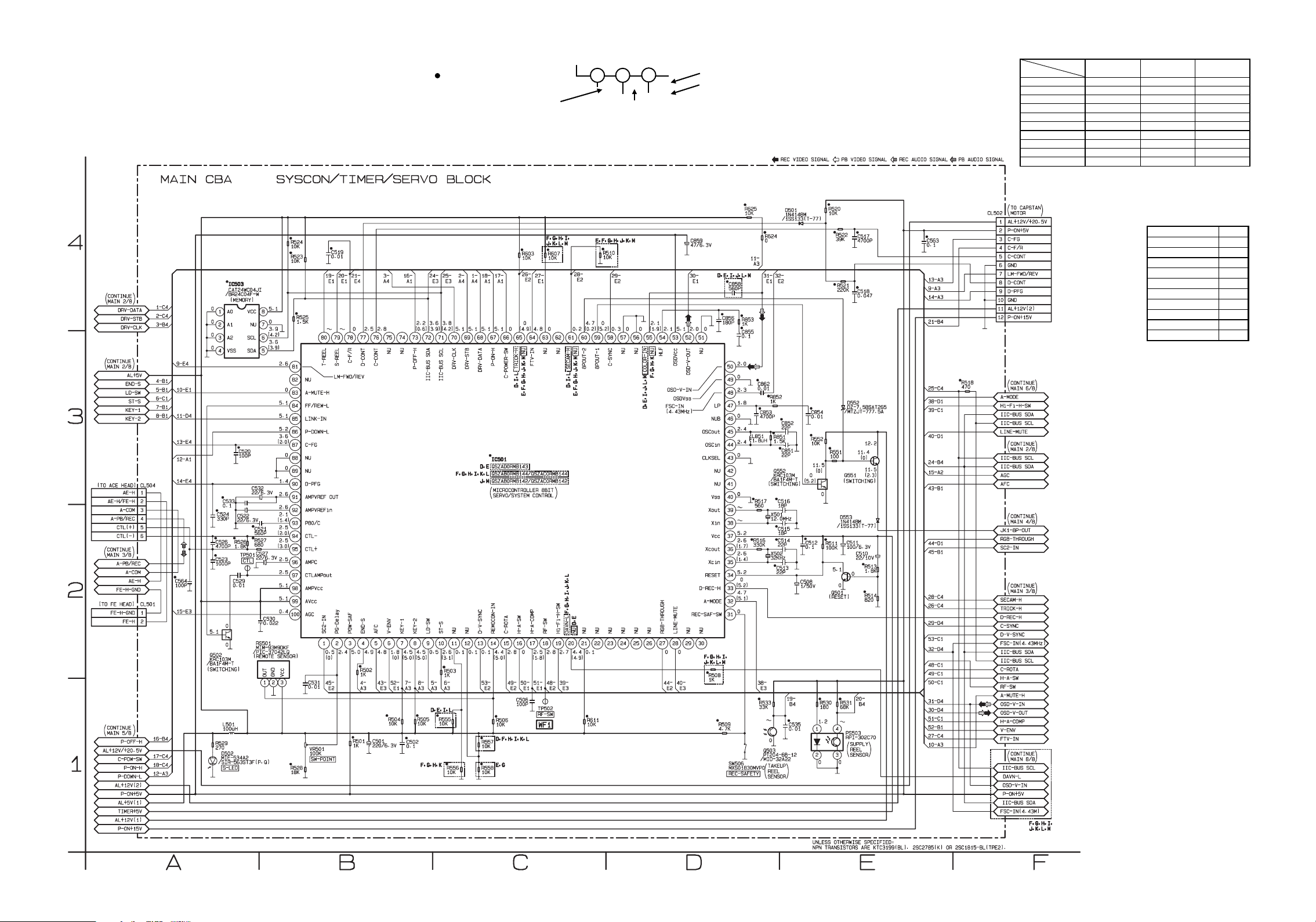
[ VR540/ (39, 58), VR740/ (02, 07, 16, 39, 58), VR742/ (16, 39, 58) ]
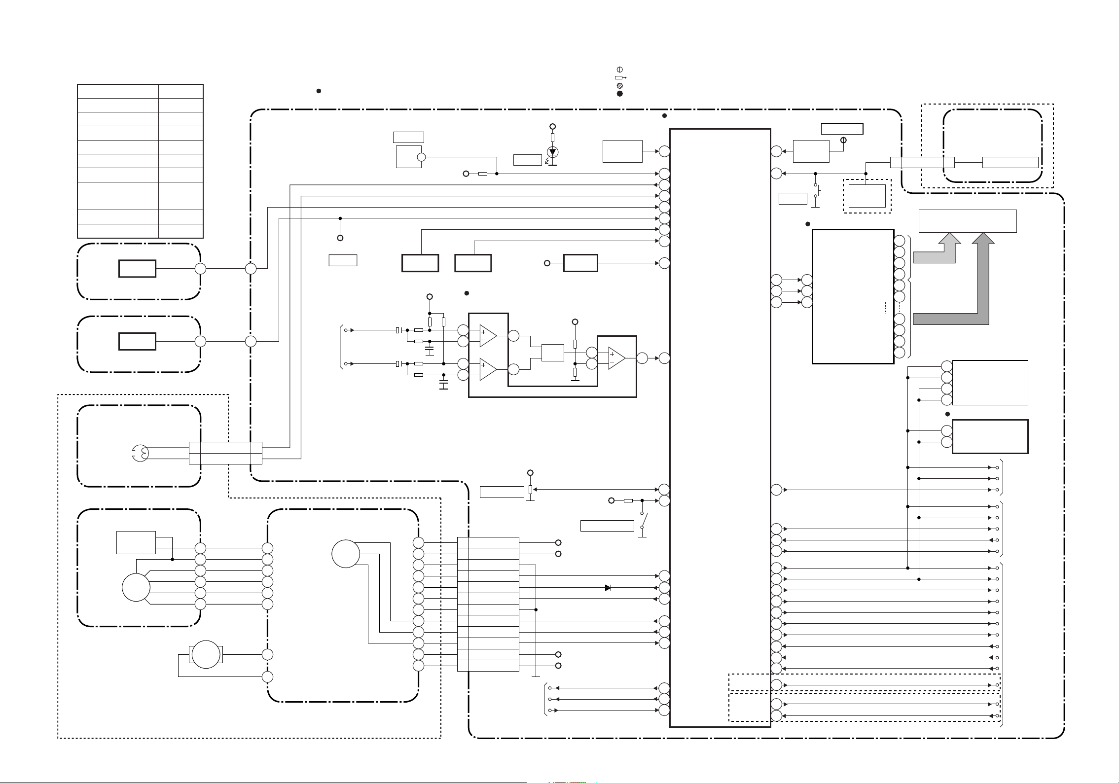
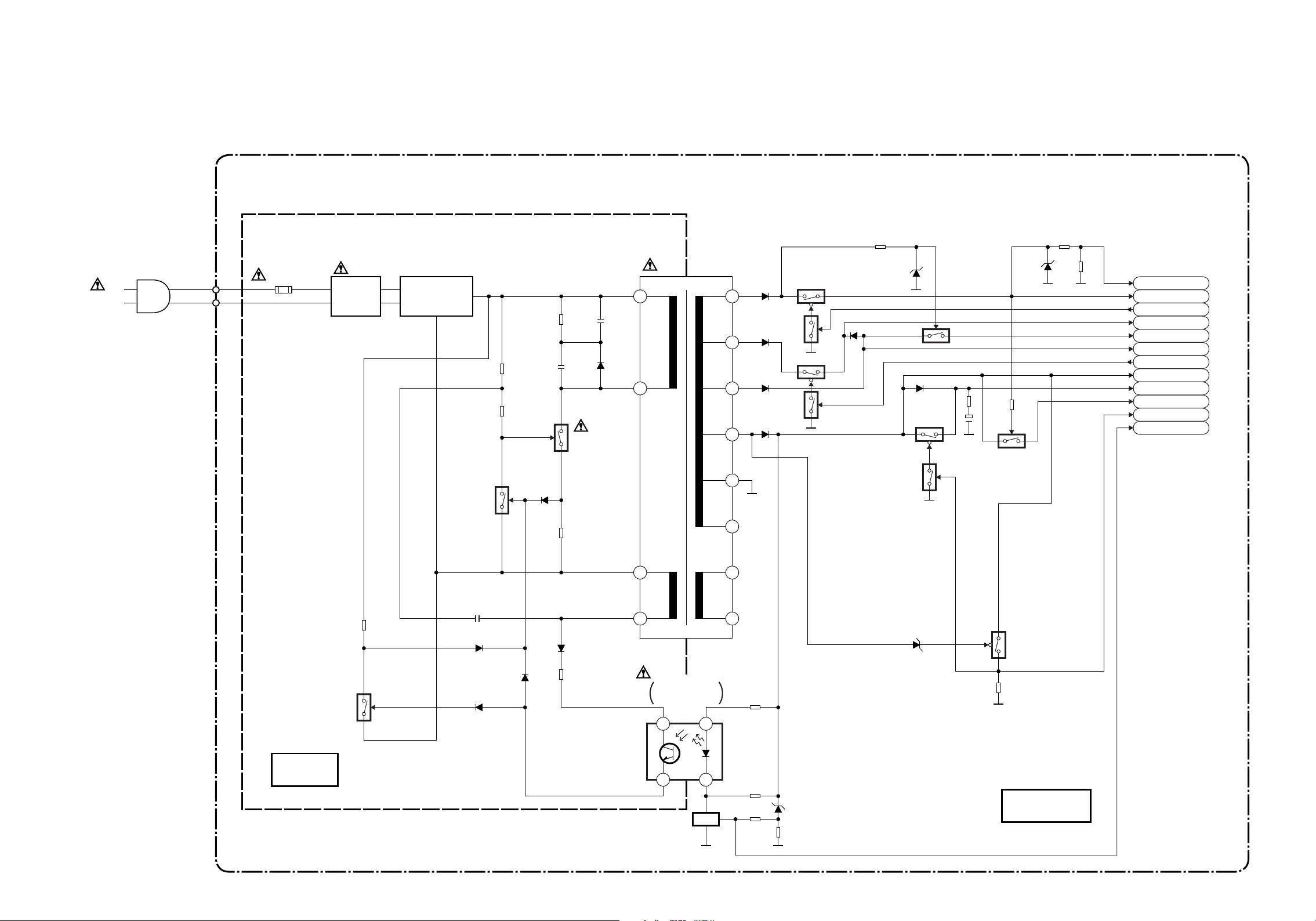
Servo/System Control Block Diagram
Comparison Chart of
Models & Marks
Model Mark
VR540/39
VR540/58
VR740/02
VR740/07 G
VR740/16
VR740/39
VR740/58
VR742/16
VR742/39
VR742/58
Q504
ST-S
SENSOR CBA
Q505
END-S
SENSOR CBA
(DECK ASSEMBLY)
AC HEAD ASSEMBLY
CONTROL
HEAD
CYLINDER ASSEMBLY CAPSTAN MOTOR
PG
SENSOR
DRUM
MOTOR
M
LOADING
MOTOR
D
E
F
H
I
J
K
L
M
CL287
5 5CTL(+)
6 6CTL(-)
M
CL504
" " = SMD
MAIN CBA
FROM
VIDEO
BLOCK
CAPSTAN
MOTOR
END-S
TU-VIDEO
V-IN1
M
NOTE FOR WIRE CONNECTORS:
1. PREFIX SYMBOL "CN" MEANS CONNECTOR.
(CAN DISCONNECT AND RECONNECT.)
2. PREFIX SYMBOL "CL" MEANS WIRE-SOLDER
HOLES OF THE PCB.
(WIRE IS SOLDERED DIRECTLY.)
SW507
LD-SW
AL+5V
Q503
T-REEL
P-ON+5V
PS503TP506
11
10
12 P-ON+15V
11
10 GND
BLOCK DIAGRAMS
AL+5V
D502
S-LED
Q501
P-ON+5V
Q771,
Q772
AND
P-ON+15V
AL+12V
P-ON+5V
AL+12V/+20.5V
C-POW-SW
P-ON-H
P-DOWN-L
RESET
4
5
AL+5V
REC-SAFETY
S-REEL
IC771
(COMPARATOR)
9
8
AL+12V(2)
D-PFG
9
D-CONT
8
LM-FWD/REV
7
GND
6
C-CONT
5
C-F/R
4
C-FG
3
P-ON+5V
2
AL+12V/+20.5V
1
TIMER+5V
VR501
SW-POINT
CL502
FROM/TO
POWER
SUPPLY
BLOCK
14
13
AL+5V
TEST POINT INFORMATION
:INDICATES A TEST POINT WITH A JUMPER WIRE ACROSS A HOLE IN THE PCB.
:USED TO INDICATE A TEST POINT WITH A COMPONENT LEAD ON FOIL SIDE.
:USED TO INDICATE A TEST POINT WITH NO TEST PIN.
:USED TO INDICATE A TEST POINT WITH A TEST PIN.
IC501
(SERVO/SYSTEM CONTROL)
RS501
REMOTE
SENSOR
2
SW506
REMOCON-IN
14
LD-SW9
95
CTL(+)
CTL(-)
94
10
ST-S
4
END-S
T-REEL
80
S-REEL79
RESET
34
FTV-IN
64
PG-DELAY
2
REC-SAF-SW
31
D-PG
90
D-CONT77
LM-FWD/REV
81
C-CONT
76
C-F/R
78
C-FG
87
C-POW-SW
66
P-ON-H
67
P-DOWN-L
86
F,G,H,I,
J,K,L,M
D,I,L
KEY- 1
KEY- 2
DRV-DATA
DRV-STB
DRV-CLK
A-MUTE-H
Hi-Fi-H-SW
A-MODE
LINE-MUTE
IIC-BUS SDA
IIC-BUS SCL
D-REC-H
RF-SW
C-ROTA
D-V SYNC
H-A-SW
H-A-COMP
V-ENV
C-SYNC
SECAM-H
7
8
SW509
ST/EJ
68
69
70
83
19
32
28
72
71
33
18
15
13
16
17
6
58
20DAVN-L
65TRICK-H
61
TP507
SENS-INH
KEY
SWITCH
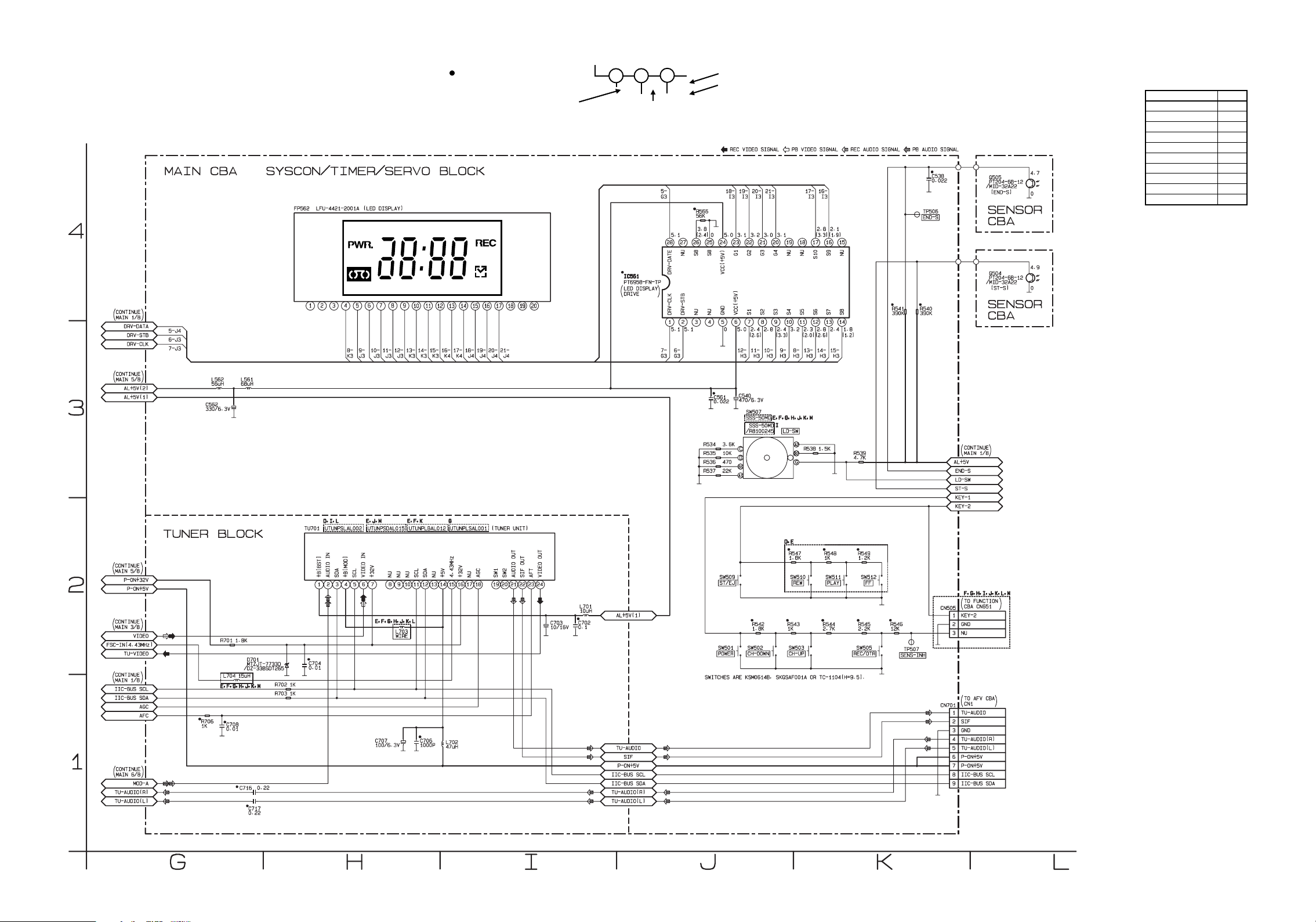
IC561 (LED DISPLAY)
DRV-DATA
28
DRV-STB
2
DRV-CLK
1
CL505 CN651
1 1KEY-2
D,E
KEY
SWITCH
G1
23
G2
22
G3
21
G4
20
S1
7
S2
8
S7
13
S8
14
S9
16
S10
17
F,G,H,I,J,K,L,M
FUNCTION CBA
KEY SWITCH
FP562
LED DISPLAY
TU701(TUNER UNIT)
SDA
3
SDA
12
SCL
5
SCL
11
IC503 (MEMORY)
SDA
5
SCL
6
IIC-BUS SDA
IIC-BUS SCL
A-MUTE-H
IIC-BUS SDA
IIC-BUS SCL
Hi-Fi-H-SW
A-MODE
LINE-MUTE
IIC-BUS SDA
IIC-BUS SCL
D-REC-H
RF-SW
C-ROTA
D-V SYNC
H-A-SW
H-A-COMP
V-ENV
C-SYNC
DAVN-L
TRICK-H
SECAM-H
TO
AUDIO BLOCK
FROM/TO
Hi-Fi AUDIO
BLOCK
FROM/TO
VIDEO BLOCK
1-9-11 1-9-12 HE473BLS
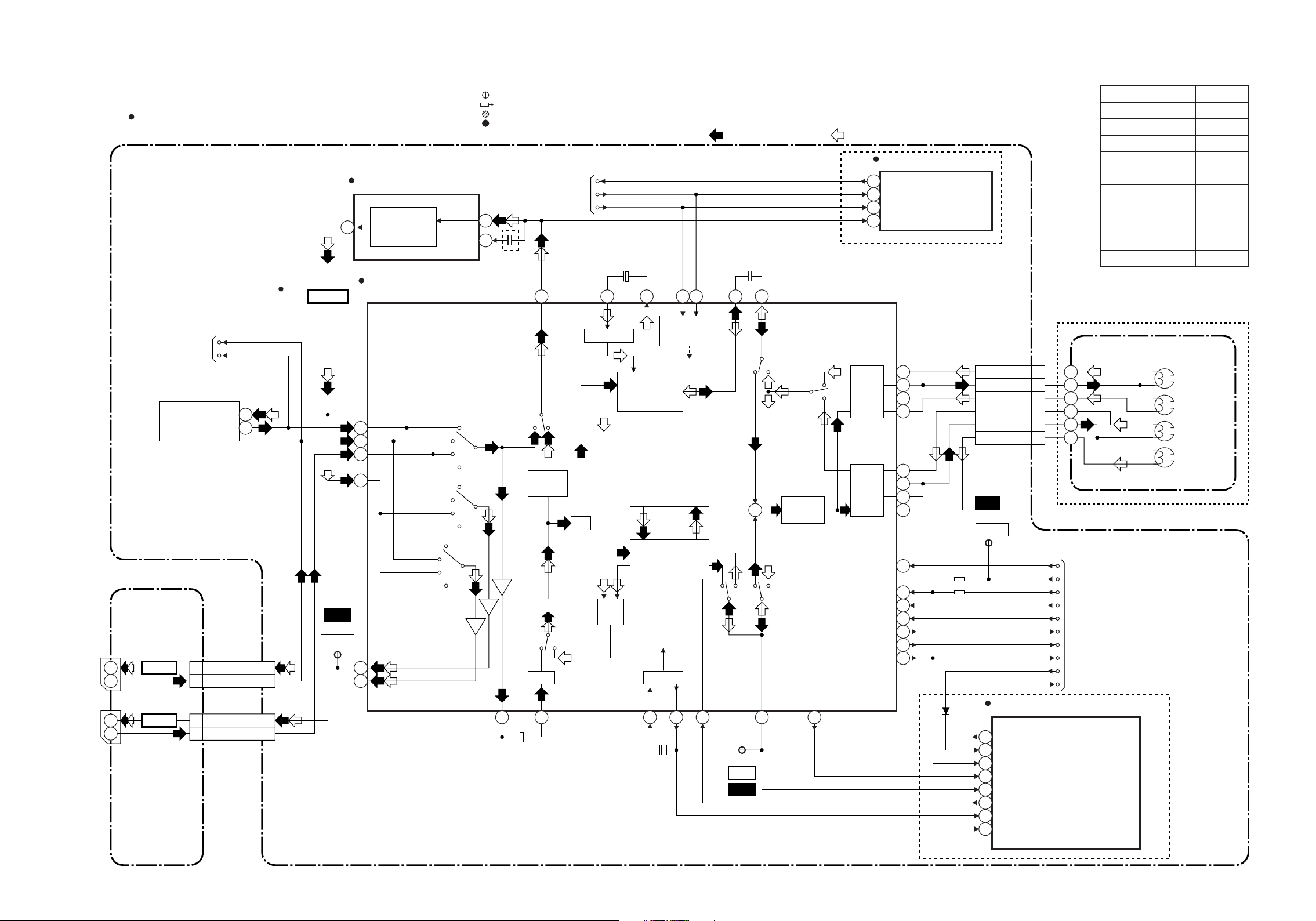
Video Block Diagram
" " = SMD
MAIN CBA
NOTE FOR WIRE CONNECTORS:
1. PREFIX SYMBOL "CN" MEANS CONNECTOR.
(CAN DISCONNECT AND RECONNECT.)
2. PREFIX SYMBOL "CL" MEANS WIRE-SOLDER
HOLES OF THE PCB.
(WIRE IS SOLDERED DIRECTLY.)
IC501 (OSD)
OSD
CHARACTER
52
MIX
IC301
Q351
BUFFER
(Y/C SIGNAL PROCESS)
TEST POINT INFORMATION
COLOR
-IN
:INDICATES A TEST POINT WITH A JUMPER WIRE ACROSS A HOLE IN THE PCB.
:USED TO INDICATE A TEST POINT WITH A COMPONENT LEAD ON FOIL SIDE.
:USED TO INDICATE A TEST POINT WITH NO TEST PIN.
:USED TO INDICATE A TEST POINT WITH A TEST PIN.
FROM
SERVO/SYSTEM
CONTROL BLOCK
50
55
D,E,I,J,L,M
65
DAVN-L
IIC-BUS SDA
IIC-BUS SCL
Comparison Chart of
Models & Marks
Model Mark
VR540/39
REC-VIDEO SIGNAL PB-VIDEO SIGNAL MODE: SP/REC
VR540/58
VR740/02
IC640 (VPS)
DAVN-L
14
6
IIC-BUS SDA
7
IIC-BUS SCL
VPS-V
16
F,G,H,I,J,K,L,M
VR740/07 G
VR740/16
VR740/39
VR740/58
VR742/16
VR742/39
VR742/58
69684643
7978
D
E
F
H
I
J
K
L
M
V-OUT1
V-IN1
V-OUT2
V-IN2
SERVO/SYSTEM
CONTROL BLOCK
JACK CBA
JK101
Q101
JK102
BUFFER
Q102
BUFFER
19
20
19
20
V-IN1TO
TU-VIDEO
TU701(TUNER UNIT)
VIDEO-IN
VIDEO-OUT
CL101
1
V-OUT1
V-IN1
3 3
CL102
1
V-OUT2
V-IN2 3
3
24
Y. DELAY
LUMINANCE
SIGNAL
PROCESS
6
48
50
52
56
WF1
J23
CL151
1
CL152
1
V-OUT
61
63
TUNER
PB/EE
TUNER
IN1
PB/EE
MUTE
IN1
IN2
FRT
IN2
FRT
MUTE
BYPASS
CHARA.
INS.
AGC VXO
58 59
FBC
AGC
CCD 1H DELAY
1/2
CHROMINANCE
SIGNAL
PROCESS
Y/C
MIX
PR
4.433619MHz
SERIAL
DECORDER
2928
X301
R
P
Y
REC FM
+
C
R P R P
25 44
TP301
C-PB
WF2
AGC
PB-H OUT
21
SP
SP
HEAD
AMP
EP
EP
HEAD
AMP
D-REC-H
C-ROTA/RF-SW
D-V-SYNC
H-A-SW
H-A-COMP
V-ENV
C-SYNC
96
95
93
94
90
89
88
87
80
70
62
71
83
84
67
CL253
V(R)-1
V-COM
V(L)-1
V(L)-2
V-COM
V(R)-2
WF1
TP502
RF-SW
D-V-SYNC
H-A-COMP
IC370 (PAL/SECAM DECTECTOR)
28
1
29
17
14
18
2
16
1
2
3
4
5
6
D-REC-H
RF-SW
C-ROTA
H-A-SW
V-ENV
C-SYNC
TRICK-H
SECAM-H
PAL/SECAM
DETECTOR
FROM/TO SERVO/SYSTEM
CONTROL BLOCK
CYLINDER ASSEMBLY
VIDEO (R)-1
HEAD
VIDEO (L)-1
HEAD
VIDEO (L)-2
HEAD
VIDEO (R)-2
HEAD
D,I,L
(DECK ASSEMBLY)
1-9-13 1-9-14 HE473BLV
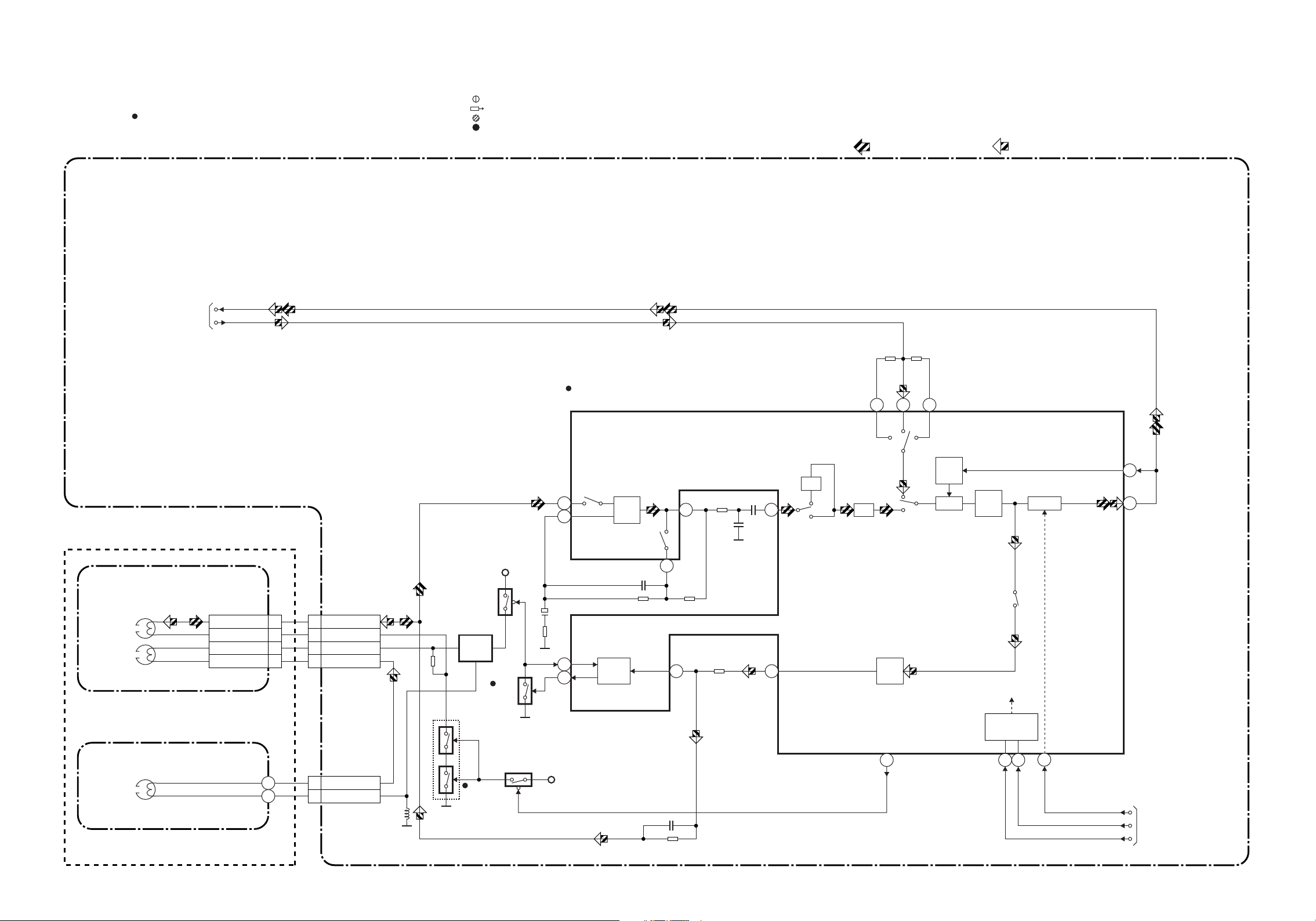
Audio Block Diagram
" " = SMD
TO Hi-Fi
AUDIO BLOCK
NOTE FOR WIRE CONNECTORS:
1. PREFIX SYMBOL "CN" MEANS CONNECTOR.
(CAN DISCONNECT AND RECONNECT.)
2. PREFIX SYMBOL "CL" MEANS WIRE-SOLDER
HOLES OF THE PCB.
(WIRE IS SOLDERED DIRECTLY.)
N-A-PB
N-A-REC
TEST POINT INFORMATION
:INDICATES A TEST POINT WITH A JUMPER WIRE ACROSS A HOLE IN THE PCB.
:USED TO INDICATE A TEST POINT WITH A COMPONENT LEAD ON FOIL SIDE.
:USED TO INDICATE A TEST POINT WITH NO TEST PIN.
:USED TO INDICATE A TEST POINT WITH A TEST PIN.
PB-AUDIO SIGNAL REC-AUDIO SIGNAL Mode : SP/REC
MAIN CBA
IC301
(AUDIO SIGNAL PROCESS) 1513 17
(DECK ASSEMBLY)
ACE HEAD ASSEMBLY
AUDIO
HEAD
AUDIO
ERASE
HEAD
FE HEAD
FULL
ERASE
HEAD
CL287
A-PB/REC 4
A-COM 3
AE-H 1
AE-H/FE-H 2
CL504
4 A-PB/REC
3 A-COM
1 AE-H
2 AE-H/FE-H
CL501
2 FE-H
1 FE-H-GND
+5V
Q401
Q402
BIAS
OSC
Q406
Q403 (SWITCHING)
Q405
(PB=ON)
5
6
1
2
+5V
PB-ON
EQ
AMP
SP/LP-ON
AUTO
BIAS
R
REC
AMP
IN1
ALC
DET
ALC
P
LINE
AMP
REC-ON
DECODER
MUTE
SERIAL
12
11
TUNER IN2
INV
98
7
3
100
ATT
AUDIO HD-SW
CONTROL
16
68 69
71
A-MUTE-H
IIC-BUS SDA
IIC-BUS SCL
TO SERVO/SYSTEM
CONTROL BLOCK
1-9-15 1-9-16 HE473BLA
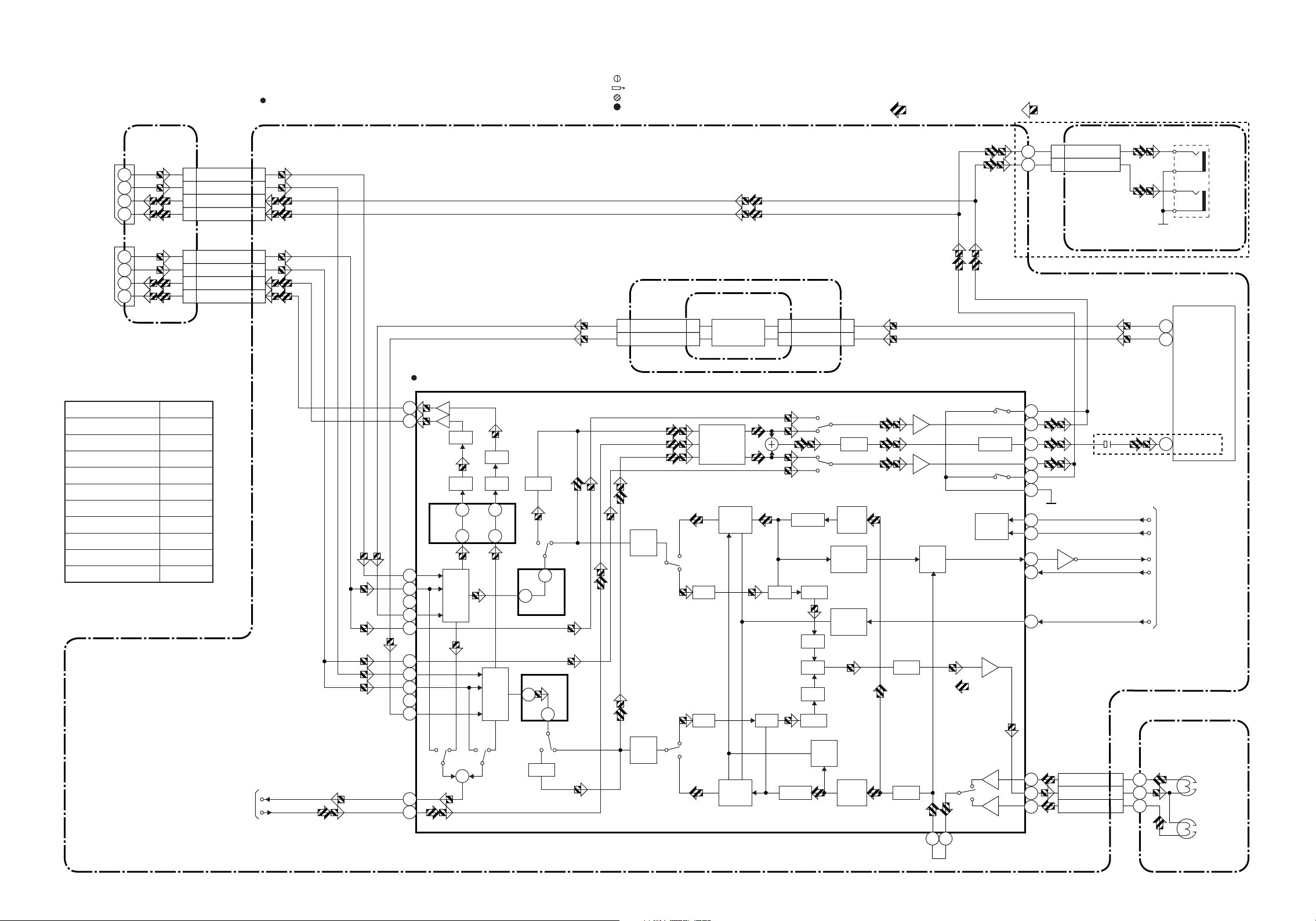
Hi-Fi Audio Block Diagram
" " = SMD
NOTE FOR WIRE CONNECTORS:
1. PREFIX SYMBOL "CN" MEANS CONNECTOR.
(CAN DISCONNECT AND RECONNECT.)
2. PREFIX SYMBOL "CL" MEANS WIRE-SOLDER
HOLES OF THE PCB.
(WIRE IS SOLDERED DIRECTLY.)
TEST POINT INFORMATION
:INDICATES A TEST POINT WITH A JUMPER WIRE ACROSS A HOLE IN THE PCB.
:USED TO INDICATE A TEST POINT WITH A COMPONENT LEAD ON FOIL SIDE.
:USED TO INDICATE A TEST POINT WITH NO TEST PIN.
:USED TO INDICATE A TEST POINT WITH A TEST PIN.
REC-AUDIO SIGNALPB-AUDIO SIGNAL Mode : SP/REC
JACK CBA
A-IN1(R)
A-IN1(L)
A-OUT1(R)
A-OUT1(L)
A-IN2(R)
A-IN2(L)
A-OUT2(R)
A-OUT2(L)
JK101
2
6
1
3
JK102
2
6
1
3
CL101
10
12
CL102
11
Comparison Chart of
Models & Marks
Model Mark
VR540/39
VR540/58
VR740/02
VR740/07 G
VR740/16
VR740/39
VR740/58
VR742/16
VR742/39
VR742/58
D
E
F
H
I
J
K
L
M
TO AUDIO BLOCK
A-IN1(R)
A-IN1(L) 8
8
6
A-OUT1(R)
A-OUT1(L) 12
9
A-IN2(R)
A-IN2(L) 8
8
6
A-OUT2(R)
A-OUT2(L) 11
10
6
9
6
CL151
CL152
N-A-REC
N-A-PB
67
65
52
56
54
50
60
2
6
10
8
4
78
80
(Hi-Fi AUDIO SIGNAL PROCESS)
IC451
SW
SW
ALC
R-CH
INSEL
ALC
62
70
61 71
L-CH
INSEL
+
48
14
ALC
ALC
47
15
MAIN CBA
CN701 CN1
4
TU-AUDIO(R)
TU-AUDIO(L)
5
R-CH
PNR
L-CH
PNR
4
5
P
R
LIM DEV
LIM DEV
R
P
AFV CBA
IF SIGNAL
PROCESS
OUTPUT
SELECT
SW
NOISE
SW
NOISE
CN1
CN701
SIF
TU-AUDIO
COMP
VCO
LPF
MIX V/I
LPF
VCO
COMP
22
11
VCO MUTE
R-CH
BPF
NOISE
DET
HOLD
PULSE
DO
DET
L-CH
BPF
LIM
ENV
DET
34 33
R
L
MUTE-ON
MUTE-ON
LOGIC
MUTE
73
74
72
76
77
75
37
38
21
53
39
24
26
27
CL509
2
A-OUT1(L)
1
A-OUT1(R)
E,F,G,H,J,K,M
IIC-BUS SDA
IIC-BUS SCL
Q451
Hi-Fi-H-SW
CL253
Hi-Fi-A(R) 9
Hi-Fi-COM 8
Hi-Fi-A(L) 7
SUB JACK CBA
A-MODE
LINE-MUTE
JK751
A-OUT
(L)
A-OUT
(R)
F,G,H,I,J,K,L,M
TU701
22
SIF OUT
21
AUDIO OUT
2
AUDIO IN
FROM/TO SYSTEM
CONTROL BLOCK
CYLINDER
ASSEMBLY
Hi-Fi
AUDIO
(R) HEAD
Hi-Fi
AUDIO
(L) HEAD
1-9-17 1-9-18
HE473BLH
Power Supply Block Diagram
AC001
NOTE :
The voltage for parts in hot circuit is measured using
hot GND as a common terminal.
HOT CIRCUIT. BE CAREFUL.
F001
T1.6A L 250V
L003
LINE
FILTER
D001 - D004
BRIDGE
RECTIFIER
CAUTION
FOR CONTINUED PROTECTION AGAINST FIRE HAZARD,
REPLACE ONLY WITH THE SAME TYPE T1.6AL/250V FUSE.
T001
Q051
2
4
Q001
12
Q052
13
Q057
14
Q058
15
CAUTION !
Fixed voltage (or Auto voltage selectable ) power supply circuit is used in this unit.
If Main Fuse (F001) is blown, check to see that all components in the power supply
circuit are not defective before you connect the AC plug to the AC power supply.
Otherwise it may cause some components in the power supply circuit to fail.
MAIN CBA
P-ON+15V
P-ON+32V
P-ON-H
Q053
Q055
Q054
AL+12V/+20.5V
AL+9V
AL+12V
C-POW-SW
AL+5V
TIMER+5V
P-ON+5V
P-DOWN-L
P-OFF-H
HOT
Q003
Q002
7
6
IC001
ERROR
VOLTAGE DET
4
Q004
(SHUNT REGULATOR)
1
23
REG
16
11
17
18
Q059
Q056
COLD
HE473BLP1-9-19 1-9-20
[ VR540/ (39, 58), VR740/ (02, 07, 16, 39, 58), VR742/ (16, 39, 58) ]
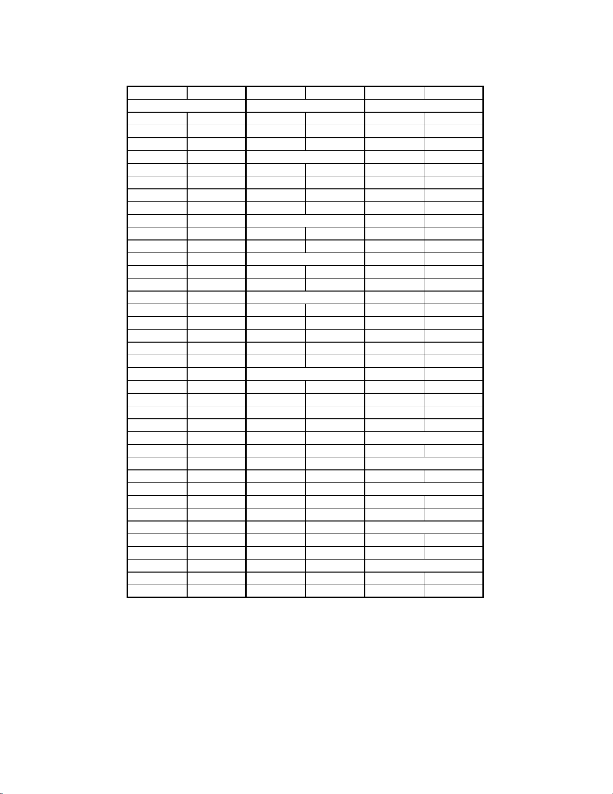
Main 1/8 Schematic Diagram Parts Location Guide
Ref No. Positio n Ref No. Position Ref No. Pos i tion
CAPACITORS
C501 B-1 CL501 A-2 R522 E-4
C502 B-1 CL502 F-4 R523 B-4
C506 C-1 CL504 A-3 R524 B-4
C508 E-2 R525 B-3
C510 E-2 D501 E-4 R526 A-2
C511 E-2 D502 A-1 R527 A-2
C512 E-2 D552 E-3 R528 B-1
C513 E-2 D553 E-2 R529 A-1
C514 E-2 R530 E-1
C515 E-2 IC501 C-3 R531 E-1
C516 E-2 IC503 A-4 R533 D-1
C517 E-4 R551 E-3
C518 E-4 L501 A-1 R552 E-3
C519 B-4 L851 D-3 R555 C-1
C520 A-3 R556 C-1
C521 A-2 Q501 E-2 R557 C-1
C522 A-2 Q502 A-2 R558 C-1
C523 A-2 Q503 D-1 R603 C-4
C524 A-2 Q551 E-3 R607 C-4
C526 A-2 Q552 D-3 R611 C-1
C527 B-2 R624 D-4
C529 A-2 R501 B-1 R625 D-4
C530 B-2 R502 B-2 R851 D-3
C531 B-1 R503 C-2 R852 D-3
C532 A-3 R504 B-1 R853 D-4
C533 A-3 R505 B-1
C535 E-1 R506 C-1 SW506 D-1
C563 E-4 R508 D-2
C564 A-2 R509 D-1 VR501 B-1
C851 E-3 R510 C-4
C852 E-3 E511 E-2 X501 D-2
C853 D-3 R513 E-2 X502 D-2
C854 E-3 R514 E-2
C855 D-3 R516 D-2 PS503 E-1
C856 D-4 R517 D-3 RS501 B-2
C858 D-4 R518 F-3
C859 D-4 R520 E-4 TP501 A-2
C862 D-3 R521 E-4 TP502 C-1
CONNECTORS
DIODES
ICS
COIL S
TRANSISTORS
RESISTORS
RESISTORS
SWITCHES
VARIABLE RESISTORS
CRYSTAL OSCILLATORS
MISCELLANEOUS
TEST PO I NTS
1-10-31
Main 1/8 Schematic Diagram
IC50 1 KEY V OLTAGE CHART
KEY 1 (7 PIN) KEY 2 (8 PIN) KEY 2 (8 PIN)
(D,E) (F,G,H,I,J,K,L)
0.00 ~ 0.51V POWER STOP/EJECT STOP/EJECT
0.51 ~ 0.92V CH DOWN REW REW
0.92 ~ 1.27V CH UP PLAY PLAY
1.27 ~ 1.61V ------------------- F F FF
1.61 ~ 1.98V ------------------- ------------------- -------------------
1.98 ~ 2.39V REC/OTR ------------------- PAUSE
2.39 ~ 2.90V ------------------- ------------------- -------------------
2.90 ~ 3.60V S-INH ------------------- -------------------
3.60 ~ 4.30V ------------------- ------------------- -------------------
4.30 ~ 5.00V KEY OFF KEY OFF KEY OFF
Comp arison Ch a rt of
Model s a nd M a rks
MODEL MARK
VR540/39 D
VR540/58 E
VR740/02 F
VR740/07 G
VR740/16 H
VR740/39 I
VR740/58 J
VR742/16 K
VR742/39 L
VR742/58 M
“ “ = SMD
MODE: SP/REC
THE SAME VOLTAGE FOR
BOTH PLAY & REC MODES.
2
1
5.0
3
5.0
~
(2.5)
INDICA TES THA T THE VOLTAGE
IS NOT CONSISTENT HERE.
PLAY MODE
REC MODE
1-10-32
1-10-33
HE473SCM1
Main 2/8 & Sensor Schematic Diagram
Comp arison Ch a rt of
Model s a nd M a rks
MODEL MARK
VR540/39 D
VR540/58 E
VR740/02 F
VR740/07 G
VR740/16 H
VR740/39 I
VR740/58 J
VR742/16 K
VR742/39 L
VR742/58 M
“ “ = SMD
MODE: SP/REC
THE SAME VOLTAGE FOR
BOTH PLA Y & REC MODES .
2
1
5.0
3
5.0
~
(2.5)
INDICA TES THA T THE VOLTAGE
IS NOT CONSISTENT HERE.
PLAY MODE
REC MODE
1-10-34
1-10-35
HE473SCM2
 Loading...