

INTEGRATED CIRCUITS
DATA SH EET
VES9600
Single Chip DVB-T Channel
Receiver
Product specification
File under Integrated Circuits, IC02
1999 Sep 01

Philips Semiconductors Product specification
Single Chip DVB-T Channel Receiver VES9600
FEATURES
• 2K and 8K COFDM demodulator ( Fully
DVB-T compliant : ETS 300-744).
• All modes supported including
hierarchical modes.
• On chip 9-bit ADC.
• Digital down conversion.
• Fully automatic transmission parameters
detection.
• Crystal or VCXO clock generation.
• Frequency offset estimator to speed up
the scan.
• RF Tuner input power measurement
• On chip FEC decoder, full DVB-T
compliant.
• Parallel or serial transport stream
interface.
• DSP based synchronization.
• BER measurement
• SNR estimation
• Channel frequency response output.
• Channel impulse response output.
• Controllable dedicated I2C tuner bus.
• 2 low frequency spare DAC. (∆Σ)
• Spare I/O.
• I2C bus interface, for easy control.
• CMOS 0.35µm technology.
DESCRIPTION
The VES9600 is a single chip channel receiver for 2K and 8K
COFDM modulated signals based on the ETSI specification (ETSI
300 744). The device interfaces directly to an IF signal, which is
sampled by a 9-bit AD converter.
The VES9600 performs all the COFDM demodulation tasks from IF
signal to the MPEG2 transport stream. An internal DSP core
manages the synchronization and the control of the demodulation
process.
After base band conversion and FFT, the channel frequency
response is estimated based on the scattered pilots, and filtered in
both time and frequency domains. This estimation is used as a
correction on the signal, carrier by carrier. A common phase error
and estimator is used to deal with the tuner phase noise.
The FEC decoder is automatically synchronized thanks to the frame
synchronization algorithm that uses the TPS information included in
the modulation. Finally descrambling according to DVB-T standard,
is achieved at the Reed Solomon output.
This device is controlled via an I2C bus. The chip provides a
switchable tuner I2C bus to be disconnected from the I2C master
when not necessary. The DSP software code can be fed to the
chip via the master I2C bus or via a dedicated I2C bus (Eeprom).
Designed in 0.35 µm CMOS technology and housed in a 208-pin
MQFP package, the VES9600 operates over the commercial
temperature range.
APPLICATIONS
• DVB-T fully compatible.
• Digital data transmission using
COFDM modulations.
1999 Sep 01 2
1999 Sep 01 3
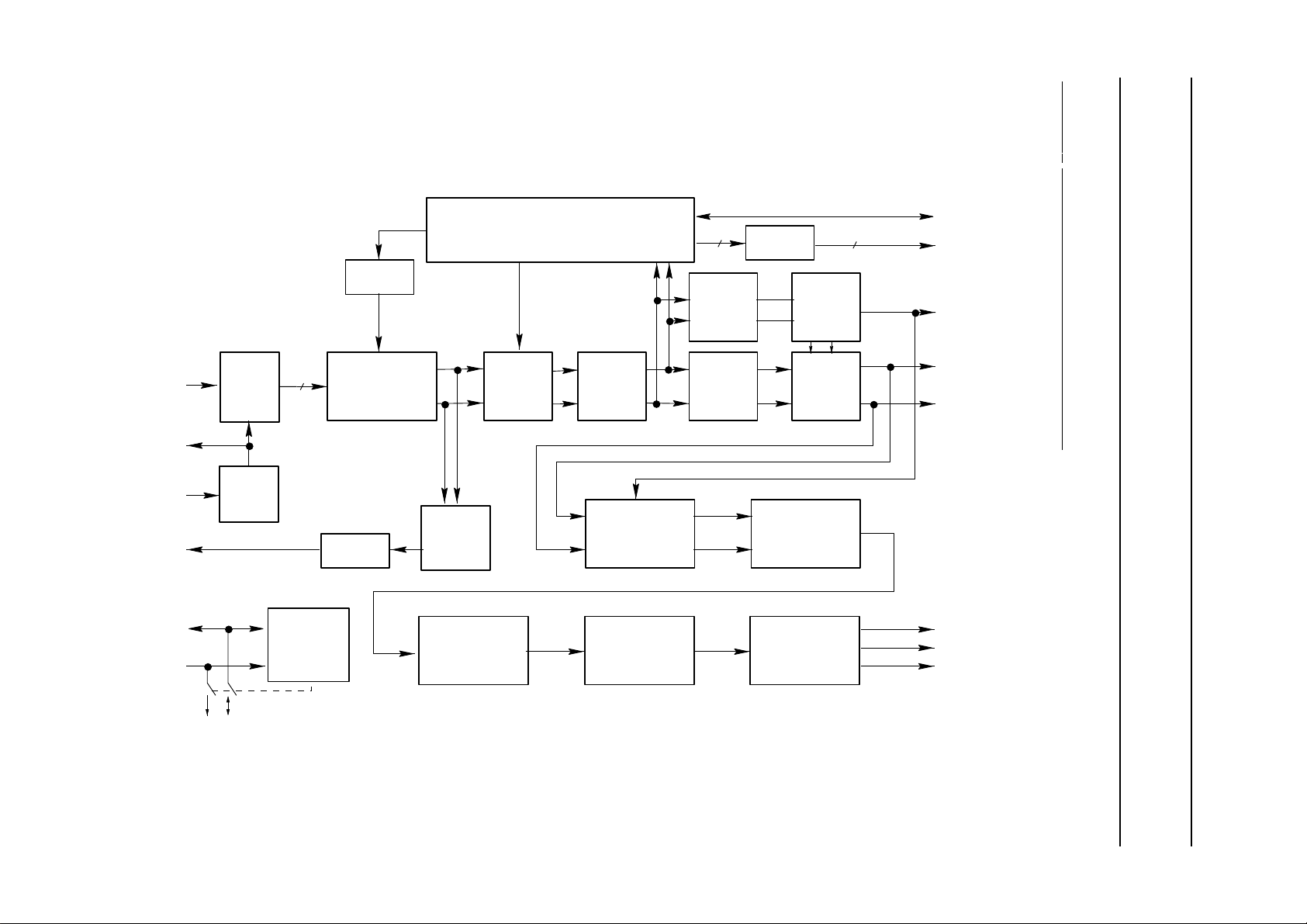
FIGURE 1 : FUNCTIONAL BLOCK DIAGRAM
Single Chip DVB-T Channel Receiver VES9600
Philips Semiconductors Product specification
IF
SACLK
XIN
O AGC
SDA
SCL
ADC
/2
9
2
IC
INTERFACE
NCO
BASE-BAND
CONVERSION
Σ/∆
OAK+ DSP CORE (XIN MIPS)
Frequency Timing framing recovery
CARRIER
RECOVERY
AGC
OUTER
DE-INTERLEAVER
FFT
INNER
DE-INTERLEAVER
R. S.
DECODER
10
CHANNEL
ESTIMATOR
CPE
3 Symbols
DELAY LINE
Σ/∆
TIMING
FREQUENCY
INTERPOLATOR
CORRECTION
VITERBI
DECODER
DE-SCRAMBLER
General purpose
digital inputs/outputs
3
analog outputs
CONFIDENCE
I
RECOV_DATA
Q
DO
OCLK
DEN
TO TUNER
Philips Semiconductors Product specification
Single Chip DVB-T Channel Receiver VES9600
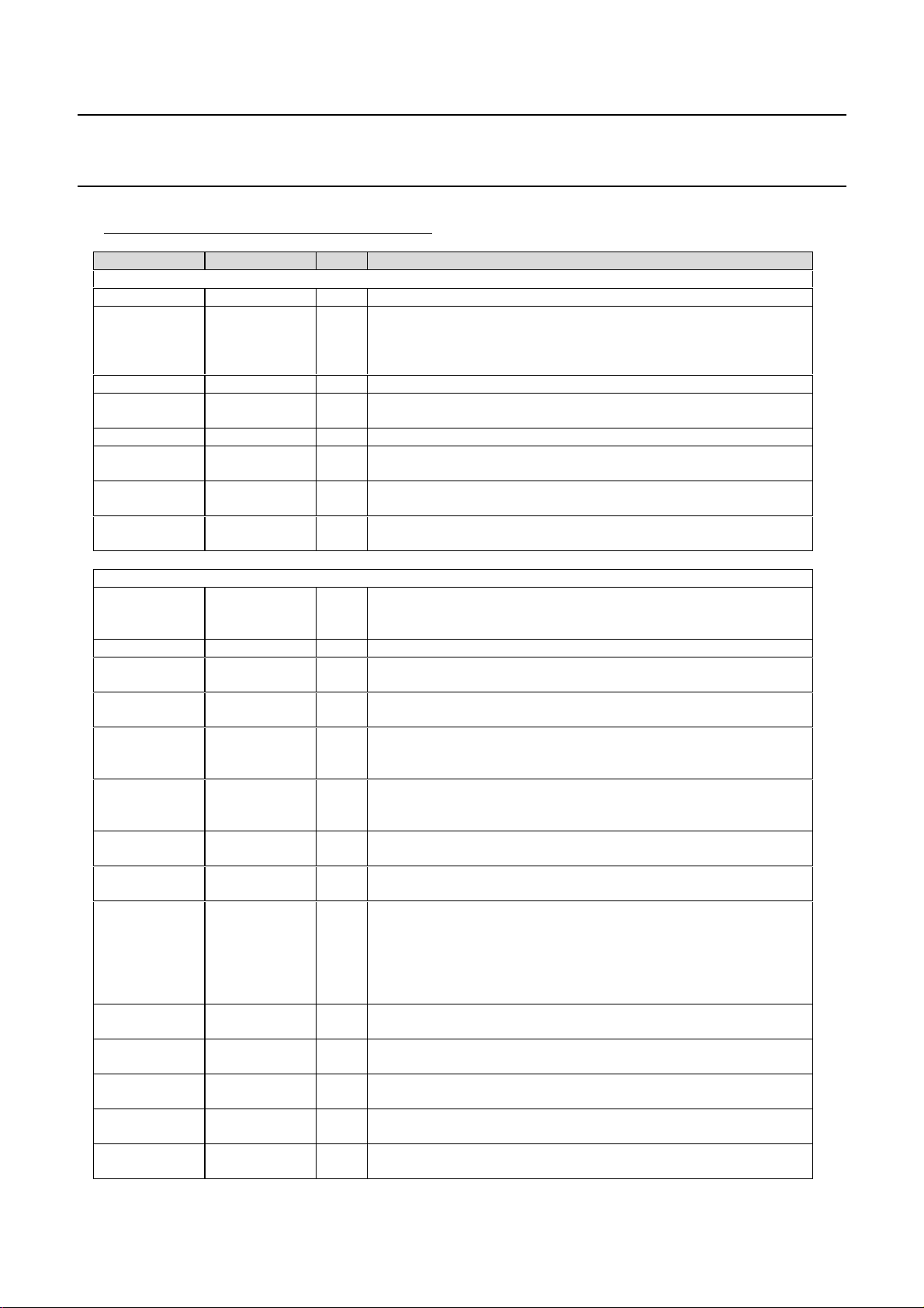
INPUT - OUTPUT SIGNAL DESCRIPTION
SYMBOL PIN NUMBER TYPE DESCRIPTION
CLOCK AND RESET SIGNALS
CLR# 32 I reset signal, active low
8
XIN
XOUT 9 O Crystal oscillator output pin.
SACLK
USE_NCO 33 I When low the chip is in VCXO mode else in NCO mode
CTRL_VCXO
CLK_X1
CLK_X2
25 O
26 O
181 O
180 O
I
(5V)
(5V)
(5V)
(5V)
Crystal oscillator input pin. When USE_NCO pin is high a third
overtone XTAL should be connected between the XIN and XOUT pins.
When USE_NCO pin is low a VCXO should be connected between
XIN and via a RC filter to the CTRL_VCXO output.
Sampling frequency output. This output clock can be fed to an
external (10-bit) ADC as sampling clock. SACLK= XIN/2
If not in NCO mode, control of an external sampling VCXO (after low-
pass filtering)
Internal SACLK equivalent monitoring output.
Internal SACLK* 2 equivalent monitoring output.
DEMODULATOR SIGNALS
FI[9:0] 12-13-14-15-16-
19-20-21-22-23
FFT_WIN_IN 81 I to be connected to FFT_WIN_OUT in default mode.
FFT_WIN_OUT 82 O
VAGC 27 O
RECOV_DATA
[7:0]
CFND[3 :0] 151-152-153-154 O
H2[3:0] 160-161-162-163 O
EN_CLK
D_START 145 O
D_VAL 144 O
FRAME 147 O
SUPER_FRAME 146 O
TPS_VAL 143 O
FEL
168-169-170171-172-173-
174-175
150 O
77 0
I Input data from an external ADC, FI must be tied to ground when not
used, positive notation (from 0 to 1023) or two’s complement notation
(from -512 to 511).
Output signal, indicating the start of the active data; equals 1 during
(3.3)
output value from the Delta-Sigma Modulator, used to control a log-
(5V)
O
Demodulator output signal (after channel correction), synchronous with
(3.3)
(3.3)
(3.3)
(3.3)
(3.3)
(3.3)
(3.3)
(3.3)
(3.3)
(5V)
the falling edge of CLK_X1, provided in a multiplexed way, I first.
Multiplexed output bearing the confidence factor during I and channel
response square amplitude during Q (4 MSB bits), respectively to
RECOV_DATA. (For the channel square amplitude see C2_H2)
4 LSB bits of the channel response square amplitude according to
enable clk18 to synchronize and phase the RECOV_DATA H2 et
CFND outputs. EN_CLK is set to 1 during I and 0 during Q.
Output signal, indicating the start of the active data out of the
equalizer; equals 1 during sample Kmin of the RECOV_DATA current
output block, for 2 18MHz clock cycles. CAUTION : sample Kmin does
not convey regular data, since it happens to be a continual carrier; it is
the first active (non zero) sample of the current OFDM block, but
active when RECOV_DATA corresponds to regular data .
Indicate the active data out of the first block in a frame at the
Same as FRAME in 8K; in 2K, active only on the first block of each
superframe. Indicates the beginning of a new SUPER-FRAME.
active when RECOV_DATA corresponds to TPS demodulated data .
front end lock. FEL is an output drain output and therefore requires an
complex sample 0 of the active FFT block
scaled amplifier (after analog filtering )
Normal order.
CFND.
D_VAL and TPS_VAL (see below) will be low.
demodulation part output. (RECOV_DATA)
external pull up resistor.
1999 Sep 01 4
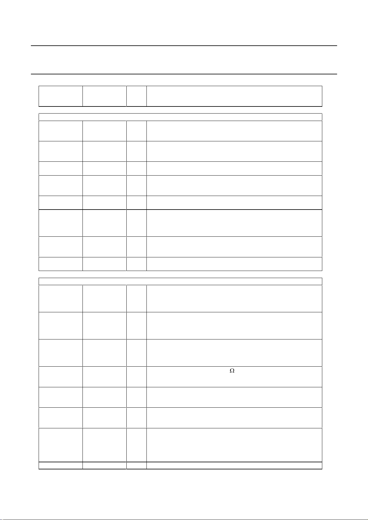
Philips Semiconductors Product specification
Single Chip DVB-T Channel Receiver VES9600
76
IT
DO[7:0] 118-119-120-
121-124-125-
126-127
OCLK 113 O
DEN 115 O
PSYNC 112 O
UNCOR 114 O
FSTART 109 O
108
DVIT
HVIT
107 O
(5V)
(3.3)
(3.3)
(3.3)
(3.3)
(3.3)
(3.3)
(3.3)
(3.3)
Interrupt line. This output interrupt line can be configured by the I2C
O
interface. See registers Itsel and Itstat. IT is an open drain output and
therefore requires an external pull up resistor.
FEC OUTPUTS
O
output data carrying the current sample of the current MPEG2 packet
(188 bytes), delivered on the rising edge of OCLK by default. When
the serial mode is selected, the output data is delivered by DO[0].
Output CLock. OCLK is the output clock for the parallel DO[7:0]
outputs. OCLK is internally generated depending on which interface is
selected.
output data validation signal active high during the valid and regular
data bytes (may be inverted, see serial bus description).
Pulse SYNChro. This output signal goes high on a rising edge of
OCLK when a synchro byte is provided, then goes low until the next
synchro byte (may be inverted).
RS error flag, active high on one RS packet if the RS decoder fails in
correcting the errors (may be inverted).
Frame start active high for one OCLK output clock cycle at the
beginning of a new superframe made of 272 OFDM symbols for the 2k
mode and made of 68 OFDM symbols for the 8k mode (may be
inverted as C3_psync).
viterbi output data stream, delivered on the rising hedge of HVIT. You
O
can also find the viterbi output on DO[0] after by-passing the RS and
the descrambling.
viterbi output data stream clock, according to DVIT.
ON-CHIP ADC SIGNALS
48
VIM
49
VIP
42
CMCAP
39
RBIAS
40
CMI
41
CMO
45
VREF
VREFP 44 O This is a positive voltage reference for the A/D converter. It is derived
I
I
I
I
O
O
O
Negative input to the A/D converter. This pin is DC biased to half
supply through an internal resistor divider (2x10K resistors). In order
to remain in the range of the ADC, the voltage difference between pins
VIP and VIM should be between -0.5 and 0.5 volts.
Positive input to the A/D converter. This pin is DC biased to half supply
through an internal resistor divider (2x10K resistors). In order to
remain in the range of the ADC, the voltage difference between pins
VIP and VIM should be between –0.5 and 0.5 volts.
This pin is connected to a tap point on an internal resistor divider used
to create CMO and CMI. An external capacitor of value 0.1µf should
be connected between this point and ground to provide good power
supply rejection from the positive supply at higher frequencies.
An external resistor of value 3.3k
pin and ground to provide good accurate bias currents for the analog
circuits on the ADC.
This pin provides the common-mode in voltage for the analog circuits
on the ADC. It is the buffered version of a voltage derived from an onchip resistor devider, and has a nominal value of 0.75 x VD3.
This pin provides the common-mode out voltage for the analog circuits
on the ADC. It is the buffered version of a voltage derived from an on-
chip resistor devider, and has a nominal value of 0.5 x VD3.
This is the output of an on-chip resistor divider. An exter nal capacitor
of value 0.1µf should be connected between this point and ground to
provide good power supply rejection from the positive supply at higher
frequencies. Reference voltages VREFP and VREFM are derived from
the voltage on VREF.
should be connected between this
1999 Sep 01 5
 Loading...