

Philips VES9600 Datasheet

PRELIMINARY
VES9600
SINGLE CHIP
DVB-T
CHANNEL RECEIVER
FEATURES
• 2K and 8K COFDM demodulator ( Fully
DVB-T compliant : ETS 300-744).
• All modes supported including
hierarchical modes.
• On chip 9-bit ADC.
• Digital down conversion.
• Fully automatic transmission parameters
detection.
• Crystal or VCXO clock generation.
• Frequency offset estimator to speed up
the scan.
• RF Tuner input power measurement
• On chip FEC decoder, full DVB-T
compliant.
• Parallel or serial transport stream
interface.
• DSP based synchronization.
• BER measurement
• SNR estimation
• Channel frequency response output.
• Channel impulse response output.
• Controllable dedicated I2C tuner bus.
• 2 low frequency spare DAC. (∆Σ)
• Spare I/O.
• I2C bus interface, for easy control.
• CMOS 0.35µm technology.
DESCRIPTION
The VES9600 is a single chip channel receiver for 2K and 8K
COFDM modulated signals based on the ETSI specification (ETSI
300 744). The device interfaces directly to an IF signal, which is
sampled by a 9-bit AD converter.
The VES9600 performs all the COFDM demodulation tasks from IF
signal to the MPEG2 transport stream. An internal DSP core
manages the synchronization and the control of the demodulation
process.
After base band conversion and FFT, the channel frequency
response is estimated based on the scattered pilots, and filtered in
both time and frequency domains. This estimation is used as a
correction on the signal, carrier by carrier. A common phase error
and estimator is used to deal with the tuner phase noise.
The FEC decoder is automatically synchronized thanks to the frame
synchronization algorithm that uses the TPS information included in
the modulation. Finally descrambling according to DVB-T standard,
is achieved at the Reed Solomon output.
This device is controlled via an I2C bus. The chip provides a
switchable tuner I2C bus to be disconnected from the I2C master
when not necessary. The DSP software code can be fed to the
chip via the master I2C bus or via a dedicated I2C bus (Eeprom).
Designed in 0.35 µm CMOS technology and housed in a 208-pin
MQFP package, the VES9600 operates over the commercial
temperature range.
APPLICATIONS
• DVB-T fully compatible.
• Digital data transmission using
COFDM modulations.
VLSI/comatlas reserves the right to make any change at anytime without notice. VES 9600 rev 1.2 / Sep 99

CAUTION
This document is preliminary and is subject to change.
Contact a VLSI Technology representative to determine if
this is the current information on this device.
The information contained in this document has been carefully checked and is believed to be reliable. However,
VLSI Technology makes no guarantee or warranty concerning the accuracy of said information and shall not be
responsible for any loss or damage of whatever nature resulting from the use of, or reliance upon, it. VLSI
Technology does not guarantee that the use of any information contained herein will not infringe upon the patent,
trademark, copyright, mask work right or other rights of third parties, and no patent or other license is implied
hereby.
This document does not in any way extend VLSI Technology warranty on any product beyond that set forth in its
standard terms and conditions of sale. VLSI Technology reserves the right to make changes in the products or
specifications, or both, presented in this publication at any time and without notice.
LIFE SUPPORT APPLICATIONS : VLSI Technology products are not intended for use as critical components in
life support appliances, devices, or systems in which the failure of a VLSI Technology product to perform could be
expected to result in personal injury.
VES9600 Data sheet
revision history
Revision number Observation
Rev1.0 Engineering document
Rev1.1 Typo errors
Rev1.2 Pin 7, 17, 70 & 200 from VCC
to VDD
VLSI/comatlas reserves the right to make any change at anytime without notice. VES 9600 rev 1.2 / Oct 99 / p2
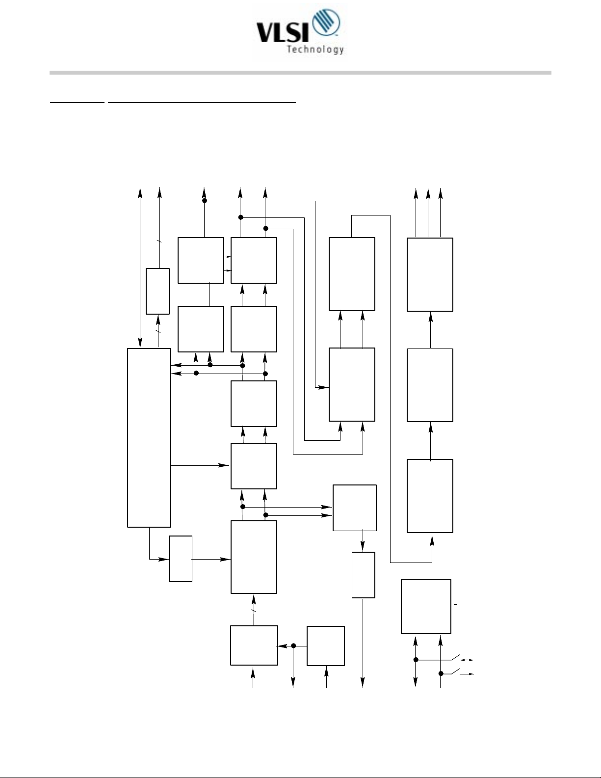
FIGURE 1 : FUNCTIONAL BLOCK DIAGRAM
General purpose
analog outputs
digital inputs/outputs
3
Σ/∆
10
CONFIDENCE
TIMING
FREQUENCY
INTERPOLATOR
CHANNEL
ESTIMATOR
CPE
I
Q
RECOV_DATA
CORRECTION
3 Symbols
DELAY LINE
FFT
VITERBI
DECODER
INNER
DE-INTERLEAVER
OCLK
DEN
DO
DE-SCRAMBLER
R. S.
DECODER
OAK+ DSP CORE (XIN MIPS)
Frequency Timing framing recovery
NCO
CARRIER
RECOVERY
BASE-BAND
CONVERSION
9
ADC
IF
SACLK
/2
XIN
AGC
Σ/∆
TO AGC
OUTER
DE-INTERLEAVER
2
IC
INTERFACE
SDA
SCL
TO TUNER
VLSI/comatlas reserves the right to make any change at anytime without notice. VES 9600 rev 1.2 / Oct 99 / p3

INPUT - OUTPUT SIGNAL DESCRIPTION
SYMBOL PIN NUMBER TYPE DESCRIPTION
CLOCK AND RESET SIGNALS
CLR# 32 I reset signal, active low
8
XIN
XOUT 9 O Crystal oscillator output pin.
SACLK
USE_NCO 33 I When low the chip is in VCXO mode else in NCO mode
CTRL_VCXO
CLK_X1
CLK_X2
FI[9:0] 12-13-14-15-16-
FFT_WIN_IN 81 I to be connected to FFT_WIN_OUT in default mode.
FFT_WIN_OUT 82 O
VAGC 27 O
RECOV_DATA
[7:0]
CFND[3 :0] 151-152-153-154 O
H2[3:0] 160-161-162-163 O
EN_CLK
D_START 145 O
D_VAL 144 O
FRAME 147 O
SUPER_FRAME 146 O
TPS_VAL 143 O
FEL
25 O
26 O
181 O
180 O
19-20-21-22-23
168-169-170171-172-173-
174-175
150 O
77 0
I
(5V)
(5V)
(5V)
(5V)
I Input data from an external ADC, FI must be tied to ground when not
(3.3)
(5V)
O
(3.3)
(3.3)
(3.3)
(3.3)
(3.3)
(3.3)
(3.3)
(3.3)
(3.3)
(5V)
Crystal oscillator input pin. When USE_NCO pin is high a third
overtone XTAL should be connected between the XIN and XOUT pins.
When USE_NCO pin is low a VCXO should be connected between
XIN and via a RC filter to the CTRL_VCXO output.
Sampling frequency output. This output clock can be fed to an
external (10-bit) ADC as sampling clock. SACLK= XIN/2
If not in NCO mode, control of an external sampling VCXO (after low-
pass filtering)
Internal SACLK equivalent monitoring output.
Internal SACLK* 2 equivalent monitoring output.
DEMODULATOR SIGNALS
used, positive notation (from 0 to 1023) or two’s complement notation
(from -512 to 511).
Output signal, indicating the start of the active data; equals 1 during
complex sample 0 of the active FFT block
output value from the Delta-Sigma Modulator, used to control a log-
scaled amplifier (after analog filtering )
Demodulator output signal (after channel correction), synchronous with
the falling edge of CLK_X1, provided in a multiplexed way, I first.
Normal order.
Multiplexed output bearing the confidence factor during I and channel
response square amplitude during Q (4 MSB bits), respectively to
RECOV_DATA. (For the channel square amplitude see C2_H2)
4 LSB bits of the channel response square amplitude according to
CFND.
enable clk18 to synchronize and phase the RECOV_DATA H2 et
CFND outputs. EN_CLK is set to 1 during I and 0 during Q.
Output signal, indicating the start of the active data out of the
equalizer; equals 1 during sample Kmin of the RECOV_DATA current
output block, for 2 18MHz clock cycles. CAUTION : sample Kmin does
not convey regular data, since it happens to be a continual carrier; it is
the first active (non zero) sample of the current OFDM block, but
D_VAL and TPS_VAL (see below) will be low.
active when RECOV_DATA corresponds to regular data .
Indicate the active data out of the first block in a frame at the
demodulation part output. (RECOV_DATA)
Same as FRAME in 8K; in 2K, active only on the first block of each
superframe. Indicates the beginning of a new SUPER-FRAME.
active when RECOV_DATA corresponds to TPS demodulated data .
front end lock. FEL is an output drain output and therefore requires an
external pull up resistor.
VLSI/comatlas reserves the right to make any change at anytime without notice. VES 9600 rev 1.2 / Oct 99 / p4
 Loading...