Philips ves1848 DATASHEETS

INTEGRATED CIRCUITS
DATA SH EET
VES1848
Single Chip DAVIC/DVB-RC Cable
Modem
Product specification
File under Integrated Circuits, IC02
1999 Jul 01

Philips Semiconductors Product specification
Single Chip DAVIC/DVB-RC Cable Modem VES1848
FEATURES
Fully compliant ETS300800 and DA VIC 1.2
•
Out-Off Band demodulation scheme :
•
On chip 7-bit ADC.
-
DQPSK demodulator.
-
Roll-off factor = 0.3 .
-
Direct IF sampling.
-
Variable bit rate from 1 to 12 Mbit/s (SAW
-
@ 8MHz BW).
Automatic Gain Control PWM output.
-
Descrambler.
-
Frame synchronization.
-
Deinterleaver.
-
RS decoder (55,53) .
-
In Band scheme :
•
Parallel or serial MPEG2 Transport Stream
-
inputs.
MAC PID filtering.
-
DAVIC ATM cells transmission supported.
-
Up-Stream synchronizati on.
•
Up-Stream modulation scheme :
•
Burst QPSK/16QAM modulator.
-
Roll-off factor = 0.25/0.3 .
-
Programmable preamble value.
-
- Programmable burst length.
- Direct IF synthesys from 5 to 46 MHz.
- I and Q base band outputs provided.
- Variable bit rate from 256kbit/s to 16Mbit/s.
- Programmable RS encoder.
- Scrambler.
- On chip 10 bit DACs.
• External MAC functionality.
• Package 208 MQFP.
• CMOS technology (0.35µm, 3.3V).
APPLICATIONS
Cable modem.
•
DVB interactive set-top bo x.
•
DAVIC ATM cable physical layer.
•
DESCRIPTION
Based on the DVB-RC cable and DAVIC
specifications, the VES 1848 allows interactive
communication through HFC network between settop boxes and headends.
For Down Stream (DS) channel the circuit
implements a differe ntial QPSK dem odulator (Out Of
Band application) and accepts MPEG2 Transport
Stream inputs from a DS QAM demodul ator (In Band
application). This channel allows to synchronize the
Up Stream (US) channe l and to provide data to the
MAC layer which remains external.
The US channel is highly programmable and built
around a digital burst QPSK or 16QAM modulator
with direct IF synthesys or I and Q base band
outputs. The modulator is fully DVB and MCNS
compliant thanks to its burst profile programmation
(burst length, preamble, RS encoder, scrambler, bit
rate …).
The VES 1848 is packaged in a 208 MQFP, and
operates over the commercial temperature 0-70°C.
1999 Jul 01 2

Philips Semiconductors Product specification
Single Chip DAVIC/DVB-RC Cable Modem VES1848
1 GENERAL DESCRIPTION
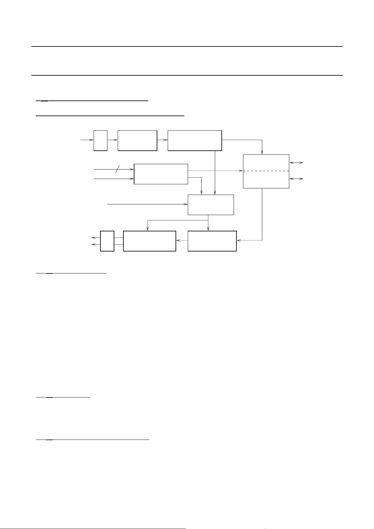
FIGURE 1 : FUNCTIONAL BLOCK DIAGRAM
fixed
ADC
IF
MPEG2-TS
symbol clock
external
synchro
programmable
IF or I
DAC
Q
demodulator
In Band
channel processing
QPSK / 16QAM
burst modulator
Out Of BandDQPSK
channel processing
Up Stream
synchronisation
Up Stream
channel encoding
1.1 ABREVIATIONS
AGC Automatic Gain Control
BW Bandwidth
CRC Cyclic Redundancy Checking (type of error correction code)
DS Down Stream (from the Headend to the set-top box)
HE Headend
HEC Header Error Control (CRC of the ATM cell header)
IB In Band
IF Intermediate Frequency
NIU Network Interface Unit (physical and MAC layers of the STB)
OOB Out Of Band
PWM Pulse Wave Modulation
SL-ESF Signalling Link Extended SuperFrame (name of the OOB frame)
STB Set-Top Box
US Up Stream (from the set-top box to the headend)
UW Unique Wor d (=pre am ble)
MAC
interface
application layers
interface
1.2 NOTATION
References to programmation registers are done this way :
AD.7 = bit 7 (in decimal) of the register located at the address AD (in hexa).
AD.[7-5] = bits 7 down to 5 of the register located at the address AD.
1.3 FUNCTIONAL DESCRIPTION
½ ADC
The VES 1848 implements a 7-bit analog to digit al converter. It directly sample s the OOB IF signal. The IF v alue
can be chosen by the system designer .
1999 Jul 01 3

Philips Semiconductors Product specification
Single Chip DAVIC/DVB-RC Cable Modem VES1848
½ DQPSK DEMODULATOR
Fully digital variable bitrate demodulator used for the OOB channel. It implements a digital down conversion to
base band, filtering and decimat ion, frequency and clock recoveries a s well as equali zation. It also provides an
AGC command to the OOB tuner.
½ OOB CHANNEL PROCESSING
After descrambling, defr aming and deinter leaving, ATM ce lls are fed into the RS decoder and correc ted. A filter ing
on ATM headers and MAC headers is the n d one on va li d c el l s to ke ep onl y t ho se addr e s sed to t he STB . MAC cells
and application layers cell s are stored in 2 diff erent FIFOs. Up to 4 different VPI-VCI can b e filtered f or applicatio n
layers data.
Mbits and Rxbits
For US synchronization, 3ms mar k ers ar e generated.
½ IB CHANNEL PROCESSING
This block is fed with the outputs of a cable FEC d ecoder . It i mp lem ent s t he f ilt er ing of the M AC d ata addr e s sed to
the STB as well as valid time references and valid Rxbits filtering.
Mbits, Rxbits (after integrity checking) and MAC data are stored in a FIFO.
For US synchronization, 3ms mar k ers ar e generated.
No PID filtering is done for application layers data.
This block implements the filtering of ATM cells transported in MPEG2-TS packet as defined by DAVIC. These data
are stored in the application layers FIFO and up to 4 different VPI-VCI can be filtered.
(1)
are also output after integrity checking.
½ INTERFACES
MAC messages and applicati on layers data are stored in different FIFOs. They can then be read/write with the
same or 2 different micro processor interfaces.
The VES 1848 registers are programmed with the MAC interface.
½ US SYNCHRONIZATION
This block decides when to send an US burst.
When the VES 1848 is used in a DVB/DAVIC device , th is bloc k al so doe s t he propagation dela y com pen sa tio n a nd
the US slot numberin g. It uses information fr om the DS channel (Mb its, 3ms markers) an d some provided by the
MAC layer (time compensation, slot number where to send a burst).
When the US path is u sed in a MCNS device, the burst start inf ormation is prov ided by the toggle of the external
synchro pin.
½ US CHANNEL ENCODING
It is DVB/DAVIC and MCNS compliant than ks to its burst profile programmatio n (6 different profiles ca n be stored
in the VES 1848).
Data read in FIFOs are RS encoded, randomized and differential encode d before the addit ion of a programmabl e
preamble.
½ BURST MODULATOR
Data can be output either in base band after predistorsion and nyquist filtering or directly on a programmable IF. In
that case a programmable sinewav e can al so be gen erated if required.
½ DAC
Two 10-bit Digital to Analog Converters are built in the VES 1848. The modulated data are provided on both analog
and digital outputs.
(1)
refer to the DVB or DAVIC specification for the definition of Mbits and Rxbits.
1999 Jul 01 4

Philips Semiconductors Product specification
Single Chip DAVIC/DVB-RC Cable Modem VES1848
TABLE 1: ABSOLUTE MAXIMUM RATINGS
Parameter Min Max Unit
Ambient operating temperature : Ta 0 70 °C
DC supply voltage (VDD) - 0.5 + 4.1 V
DC Input voltage - 0.5 VDD + 0.5 V
DC Input Current ± 20 mA
Lead Temperature +300 °C
Junction Temperature +150 °C
Stresses above the absolute m axim um rat in gs ma y caus e perm ane nt dam age to the de vi ce. E xpo sure to
absolute maximum ratings conditions for extended periods may affect device reliability.
TABLE 2 : RECOMMENDED OPERATING CONDITIONS
Symbol Parameter Min Typ Max Unit Notes
VDD
VD1, VD1IQ
VCC 5V supply 4.75 5 5.25 V
Ta Operating temperature 0 70 °C Ambient temperature
(1)
VIH
VIL Low-level input voltage -0.5 0.8 V TTL input
(2)
VOH
VOL Low-level output vo ltage 0.1
IDD + ICC Supply current 300 mA @US_clk = 116MHz
CIN Input capacitance 15 pF
COUT Output capacitance 15 pF
VD2
VD3, VD4
AVDDI, AVDDQ
VD0I, VD0Q
I
FS
R
L
Digital supply voltage 3.14 3.3 3.46 V 3.3V ±5%
5V ± 5%
High-level input voltage 2 VCC + 0.3 V TTL input
High-level output voltage VDD -0.1
2.4
V @ IOH = -0.8 mA
@ IOH = + 2mA
V @ IOL = 0.8 mA
0.4
@ IOL = + 2mA
(3)
Analog supply voltage 3.14 3.3 3.46 V 3.3V ± 5%
DAC full scale output
25 mA
current range
DAC termination resistor 75 ohms
(1)
All inputs are 5V tolerant.
(2)
IOH, IOL = ± 4mA only for pins DATAA, DATAM, INTA, INTM, VAGC, PWM2, FCONTI, SDAOUT, SDAIN,
SCLOUT, WRNA, RDN_ENAA, CSA, US_SA CL K.
(3)
with the US modul ator worki ng in continuous mode and with direct IF synthesys.
1999 Jul 01 5

Philips Semiconductors Product specification
Single Chip DAVIC/DVB-RC Cable Modem VES1848
TABLE 3 : ANALOG CHARACTERISTICS
Symbol Parameter Min Typ Max Unit Notes
VIP-VIM ADC input signal range -0.5 0.5 V
ADC Rin ADC input Resistance 3 kohms
ADC Cin ADC capacitance
(VIP or VIM)
ADC BW OOB ADC input full
power bandwidth
I
FS147
Voc DAC output voltage
SFRD DAC spurious Free
DAC full scale output
current
(on Iana and Qana)
compliance
Dynamic Range
40 50 MHZ 0.1dB bandwith
17 18 19 mA VrefIQ=1.235V
0 1.0 1.05 V
510pf
US_clk = 60MHz
-50 DBc RL = 37.5 ohms
US_clk = 58 MHz
IrefI and irefQ
connected to a
147Ω resistor,
Vout ≤ 1.0V
R
≤ 75 ohms
L
Input data
frequency
= 0.3 US_clk
1999 Jul 01 6
 Loading...