comatlas S.A., 30 rue du Chêne Germain, BP 814, 35518 CESSON SEVIGNE Cedex, France
Phone : + 33 2 99 27 55 55 – Fax : +33 2 99 27 55 27, Internet : www.comatlas.fr / VES 1848 rev 1.2 / July 99
VES 1848
SINGLE CHIP
DAVIC / DVB-RC
CABLE MODEM
FEATURES
•
Fully compliant ETS300800 and DA VIC 1.2
•
Out-Off Band demodulation scheme :
-
On chip 7-bit ADC.
-
DQPSK demodulator.
-
Roll-off factor = 0.3 .
-
Direct IF sampling.
-
Variable bit rate from 1 to 12 Mbit/s (SAW
@ 8MHz BW).
-
Automatic Gain Control PWM output.
-
Descrambler.
-
Frame synchronization.
-
Deinterleaver.
-
RS decoder (55,53) .
•
In Band scheme :
-
Parallel or serial MPEG2 Transport Stream
inputs.
-
MAC PID filtering.
-
DAVIC ATM cells transmission supported.
•
Up-Stream synchronizati on.
•
Up-Stream modulation scheme :
-
Burst QPSK/16QAM modulator.
-
Roll-off factor = 0.25/0.3 .
-
Programmable preamb le valu e.
- Programmable burst length.
- Direct IF synthesys from 5 to 46 MHz.
- I and Q base band outputs provided.
- Variable bit rate from 256kbit/s to 16Mbit/s.
- Programmable RS encoder.
- Scrambler.
- On chip 10 bit DACs.
• External MAC functionality.
• Package 208 MQFP.
• CMOS technology (0.35µm, 3.3V).
APPLICATIONS
•
Cable modem.
•
DVB interactive set-top box.
•
DAVIC ATM cable physical layer.
DESCRIPTION
Based on the DVB-RC cable and DAVIC
specifications, the VES 1848 allows interactive
communication through HFC network between settop boxes and headends.
For Down Stream (DS) channel the circuit
implements a differe ntial QPSK dem odulator (Out Of
Band application) and accepts MPEG2 Transport
Stream inputs from a DS QAM demodul ator (In Band
application). This channel allows to synchronize the
Up Stream (US) cha nnel and to provide data to the
MAC layer which remains external.
The US channel is highly programmable and built
around a digital burst QPSK or 16QAM modulator
with direct IF synthesys or I and Q base band
outputs. The modulator is fully DVB and MCNS
compliant thanks to its burst profile programmation
(burst length, preamble, RS encoder, scrambler, bit
rate …).
The VES 1848 is packaged in a 208 MQFP, and
operates over the commercial temperature 0-70°C.

comatlas reserves the right to make any change at any time without notice. VES 1848 rev 1.2 / July 99 / p 2
SUMMARY
CAUTION
This document is preliminary and is subject to change. Contact a
comatlas representative to determine if this is the current information
on this device.
The information containe d in this docu ment has bee n carefully ch ecked and is believed to be reliable. How ever,
comatlas makes no guarantee or warranty concerning the accuracy of said information and shall not be
responsible for any loss or damage of whate ver nature resulting fr om the use of, or reli ance upon, it. comatlas
does not guarantee that the use of an y informat ion contained herein wil l not infringe upon the p atent, tradem ark,
copyright, mask work right or other rights of third parties, and no patent or other license is implied hereby.
This document does not in any way extend comatlas warranty on any product beyond that set forth in its
standard terms and conditions of sale. comatlas reserves the right to make changes in the products or
specifications, or both, presented in this publication at any time and without notice.
LIFE SUPPORT APPLICATIONS : comatlas products are not intended for use as critical components in life
support applian ces, devic es, or sy stems i n which t he failur e of a comatlas product to perform could be expe cted
to result in personal injury.

comatlas reserves the right to make any change at any time without notice. VES 1848 rev 1.2 / July 99 / p 3
1 GENERAL DESCRIPTION
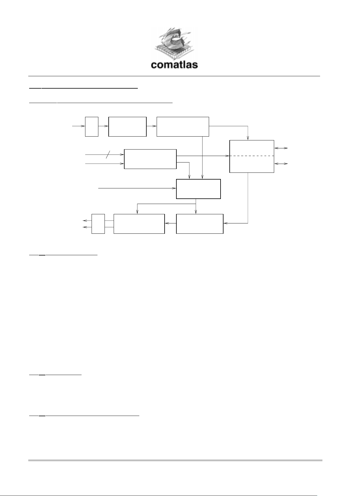
FIGURE 1 : FUNCTIONAL BLOCK DIAGRAM
interface
application layers
interface
MAC
Up Stream
synchronisation
external
synchro
channel processing
Out Of BandDQPSK
demodulator
ADC
IF
fixed
QPSK / 16QAM
burst modulator
DAC
Q
Up Stream
channel encoding
programmable
In Band
channel processing
symbol clock
MPEG2-TS
IF or I
1.1 ABREVIATIONS
AGC Automatic Gain Control
BW Bandwidth
CRC Cyclic Redundancy Checking (type of error correction code)
DS Down Stream (from the Headend to the set-top box)
HE Headend
HEC Header Error Control (CRC of the ATM cell header)
IB In Band
IF Intermediate Frequency
NIU Network Interface Unit (physical and MAC layers of the STB)
OOB Out Of Band
PWM Pulse Wave Modulation
SL-ESF Signalling Link Extended SuperFrame (name of the OOB frame)
STB Set-Top Box
US Up Stream (from the set-top box to the headend)
UW Unique Word (=preamble)
1.2 NOTATION
References to programmation registers are done this way :
AD.7 = bit 7 (in decimal) of the register located at the address AD (in hexa).
AD.[7-5] = bits 7 down to 5 of the register located at the address AD.
1.3 FUNCTIONAL DESCRIPTION
½ ADC
The VES 1848 implements a 7-bit analo g to digital converter. It directly sample s the OOB IF signal. The IF value
can be chosen by the system designer .

comatlas reserves the right to make any change at any time without notice. VES 1848 rev 1.2 / July 99 / p 4
½ DQPSK DEMODULATOR
Fully digital variable bitrate demodulator used for the OOB channel. It implements a digital down conversion to
base band, filtering and decimat ion, frequency and clock recoveries as well as equalization. It also provides an
AGC command to the OOB tuner.
½ OOB CHANNEL PROCESSING
After descrambling, de framing and dein terleaving, ATM ce lls are fed into the RS decoder and correc ted. A filt ering
on ATM headers and MAC headers is the n d one on valid cells to keep onl y t hose addressed to the STB . M AC c e ll s
and application layers cell s are stored in 2 differ ent FIFOs. Up to 4 different VP I-VCI can b e filtered for applicatio n
layers data.
Mbits and Rxbits
(1)
are also output after integrity checking.
For US synchronization, 3ms mar k ers ar e gener at ed.
½ IB CHANNEL PROCESSING
This block is fed with the outputs of a cable FEC d ec oder. It i mp lem ent s t he f iltering of the MAC data addr e s sed to
the STB as well as valid time references and valid Rxbits filtering.
Mbits, Rxbits (after integrity checking) and MAC data are stored in a FIFO.
For US synchronization, 3ms mar k ers ar e gener at ed.
No PID filtering is done for application layers data.
This block implements the filtering of ATM cells transported in MPEG2-TS packet as defined by DAVIC. These data
are stored in the application layers FIFO and up to 4 different VPI-VCI can be filtered.
½ INTERFACES
MAC messages and application layers data are stored in different FIFO s. They can then be read/write with the
same or 2 different micro processor interfaces.
The VES 1848 registers are programmed with the MAC interface.
½ US SYNCHRONIZATION
This block decides when to send an US burst.
When the VES 1848 is used in a DVB/DAVIC device , th is bl oc k also doe s the propagation de la y com pen sa tion and
the US slot numberin g. It uses information fr om the DS channel (Mb its, 3ms markers) an d some provided by the
MAC layer (time compensation, slot number where to send a burst).
When the US path is u sed in a MCNS device, the burst start information is prov ided by the toggle of the external
synchro pin.
½ US CHANNEL ENCODING
It is DVB/DAVIC and MCNS compliant than ks to its burst profile programmatio n (6 different profiles can be stored
in the VES 1848).
Data read in FIFOs are RS e ncoded, rand omized and diff erential e ncoded before the addit ion of a p rogrammable
preamble.
½ BURST MODULATOR
Data can be output either in base band after predistorsion and nyquist filtering or directly on a programmable IF. In
that case a programmable sinewav e can al so be gen er ate d if requir ed .
½ DAC
Two 10-bit Digital to Analog Converters are built in the VES 1848. The modulated data are provided on both analog
and digital outputs.
(1)
refer to the DVB or DAVIC specification for the definition of Mbits and Rxbits.

comatlas reserves the right to make any change at any time without notice. VES 1848 rev 1.2 / July 99 / p 5
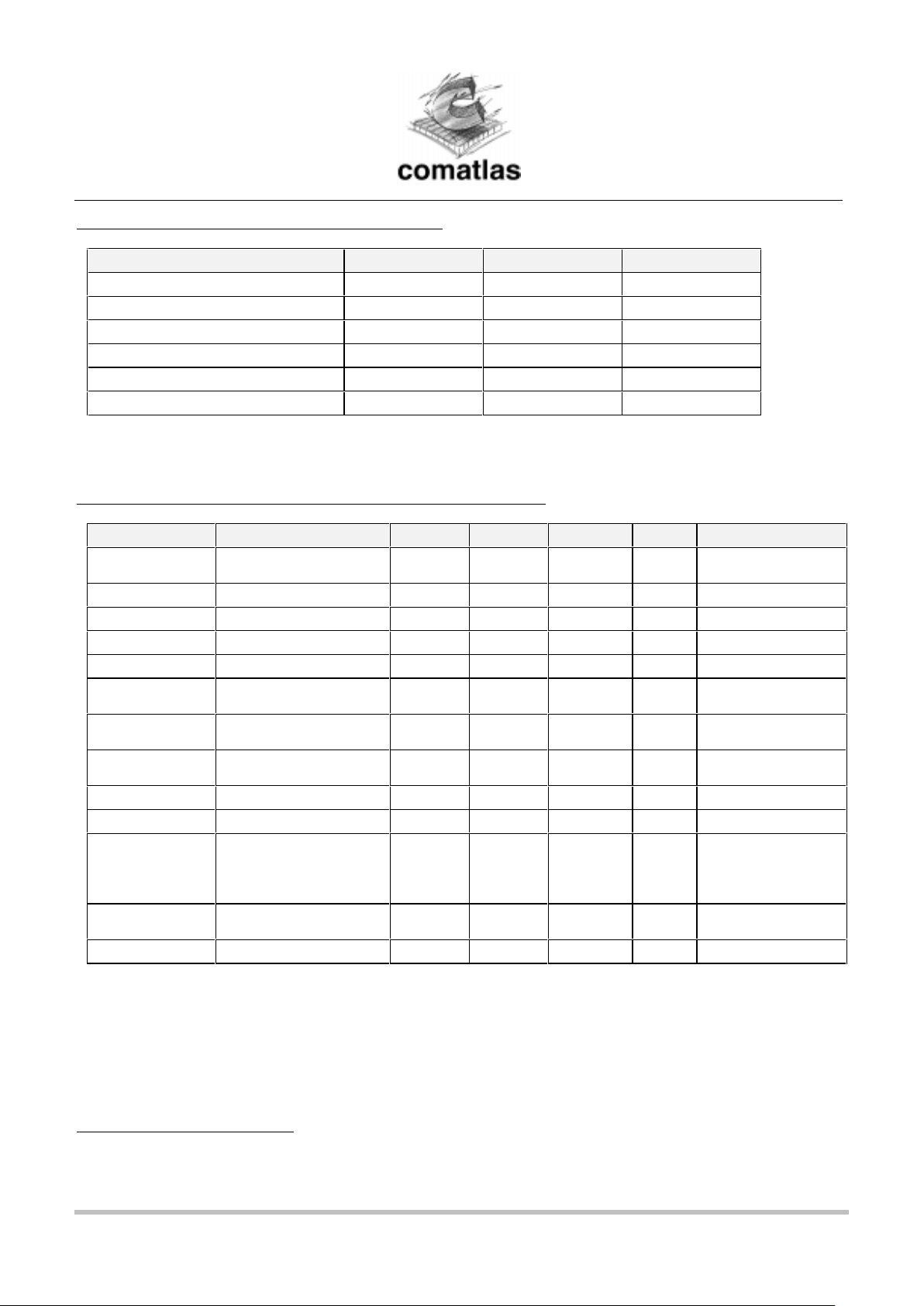
TABLE 1: ABSOLUTE MAXIMUM RATINGS
Parameter Min Max Unit
Ambient operating temperature : Ta 0 70 °C
DC supply voltage (VDD) - 0.5 + 4.1 V
DC Input voltage - 0.5 VDD + 0.5 V
DC Input Current ± 20 mA
Lead Temperature +300 °C
Junction Temperature +150 °C
Stresses above the abso lute max im um ratin gs ma y caus e perm ane nt dam age to the de vi ce. E xpo sur e to
absolute maximum ratings conditions for extended periods may affect device reliability.
TABLE 2 : RECOMMENDED OPERATING CONDITIONS
Symbol Parameter Min Typ Max Unit Notes
VDD
VD1, VD1IQ
Digital supply voltage 3.14 3.3 3.46 V 3.3V ±5%
VCC 5V supply 4.75 5 5.25 V
5V ± 5%
Ta Operating temperature 0 70 °C Ambient temperature
VIH
(1)
High-level input voltage 2 VCC + 0.3 V TTL input
VIL Low-level input voltage -0.5 0.8 V TTL input
VOH
(2)
High-level output voltage VDD -0.1
2.4
V @ IOH = -0.8 mA
@ IOH = + 2mA
VOL Low-level output voltage 0.1
0.4
V @ IOL = 0.8 mA
@ IOL = + 2mA
IDD + ICC Supply current 300 mA @US_clk = 116MHz
(3)
CIN Input capacitance 15 pF
COUT Output capacit an ce 15 pF
VD2
VD3, VD4
AVDDI, AVDDQ
VD0I, VD0Q
Analog supply voltage 3.14 3.3 3.46 V 3.3V ± 5%
I
FS
DAC full scale output
current range
25 mA
R
L
DAC termination resistor 75 ohms
(1)
All inputs are 5V tolerant.
(2)
IOH, IOL = ± 4mA only for pins DATAA, DATAM, INTA, INTM, VAGC, PWM2, FCONTI, SDAOUT, SDAIN,
SCLOUT, WRNA, RDN_ENAA, CSA, US_SACLK.
(3)
with the US modulator working in continuous mode and wit h direct IF sy nth es ys.

comatlas reserves the right to make any change at any time without notice. VES 1848 rev 1.2 / July 99 / p 6
TABLE 3 : ANALOG CHARACTERISTICS
Symbol Parameter Min Typ Max Unit Notes
VIP-VIM ADC input signal range -0.5 0.5 V
ADC Rin ADC input Resistance 3 kohms
ADC Cin ADC capacitance
(VIP or VIM)
510pf
ADC BW OOB ADC input full
power bandwidth
40 50 MHZ 0.1dB bandwith
I
FS147
DAC full scale output
current
(on Iana and Qana)
17 18 19 mA VrefIQ=1.235V
IrefI and irefQ
connected to a
147Ω resistor,
US_clk = 60MHz
Voc DAC output voltage
compliance
0 1.0 1.05 V
Vout ≤ 1.0V
R
L
≤ 75 ohms
SFRD DAC spurious Free
Dynamic Range
-50 DBc RL = 37.5 ohms
US_clk = 58 MHz
Input data
frequency
= 0.3 US_clk
 Loading...