

Philips VES1820X Datasheet
VES1820X
SINGLE CHIP
DVB-C
CHANNEL RECEIVER
FEATURES
16/32/64/128/256 QAM demodulator
•
(DVB-C compatible : ETS 300-429).
On chip 9-bit ADC.
•
On chip PLL for crystal frequency
•
multiplication.
Digital down conversion.
•
Half Nyquist filters (roll off = 15 %).
•
Automatic gain control PWM output
•
(AGC).
Symbol timing recovery, with
•
programmable second order loop filter.
Variable symbol rate capability from
•
SACLK/64 to SACLK/4
(SACLK max = 36 MHz)
Programmable anti-aliasing filters.
•
Full digital carrier recovery loop.
•
Carrier acquisition range up to 8 % of
•
symbol rate.
Integrated adaptative equalizer (Linear
•
Transversal Equalizer or Decision
Feedback Equalizer).
• On chip FEC decoder (Deinterleaver &
RS decoder), full DVB-C compliant.
• DVB compatible differential decoding
and mapping.
• Parallel or serial transport stream
interface.
• I2C bus interface, for easy control.
• CMOS 0.35µm technology.
APPLICATIONS
DVB-C fully compatible.
•
Digital data transmission using QAM modulations.
•
Cable demodulation.
•
Cable modems
•
MMDS (ETS 300-429).
•
DESCRIPTION
The VES1820X is a single chip channel receiver for 16, 32, 64, 128
and 256-QAM modulated signals. The device interfaces directly to
the IF signal, which is sampled by a 9-bit AD converter.
The VES1820X performs the clock and the carrier recovery
functions. The digital loop filters for both clock and carrier recovery
are programmable in order to optimize their characteristics
according to the current application.
After base band conversion, equalization filters are used for echo
cancellation in cable applications. These filters are configured as Tspaced transversal equalizer or DFE equalizer, so that the system
performance can be optimized according to the network
characteristics. A proprietary equalization algorithm, independent of
carrier offset, is achieved in order to assist carrier recovery. Then a
decision directed algorithm takes place, to achieve final
equalization convergence.
The VES1820X implements a FORNEY convolutional deinterleaver
of depth 12 blocks and a Reed-Solomon decoder which corrects up
to 8 erroneous bytes. The deinterleaver and the RS decoder are
automatically synchronized thanks to the frame synchronization
algorithm which uses the MPEG2 sync byte. Finally descrambling
according to DVB-C standard, is achieved at the Reed Solomon
output. This device is controlled via an I2C bus.
Designed in 0.35 µm CMOS technology and housed in a 100 pin
MQFP package, the VES1820X operates over the commercial
temperature range.
comatlas S.A., 30 rue du Chêne Germain, BP 814, 35518 CESSON-SEVIGNE Cedex, FRANCE
Phone : +33 (0)2 99 27 55 55, Fax : +33 (0)2 99 27 55 27 , Internet: www.comatlas.fr / VES 1820X rev 2.0 / Mar 99
CAUTION
This document is preliminary and is subject to change.
Contact a comatlas representative to determine if this is
the current information on this device.
The information contained in this document has been carefully checked and is believed to be reliable. However,
comatlas makes no guarantee or warranty concerning the accuracy of said information and shall not be responsible
for any loss or damage of whatever nature resulting from the use of, or reliance upon, it. comatlas does not
guarantee that the use of any information contained herein will not infringe upon the patent, trademark, copyright,
mask work right or other rights of third parties, and no patent or other license is implied hereby.
This document does not in any way extend comatlas warranty on any product beyond that set forth in its standard
terms and conditions of sale. comatlas reserves the right to make changes in the products or specifications, or
both, presented in this publication at any time and without notice.
LIFE SUPPORT APPLICATIONS : comatlas products are not intended for use as critical components in life support
appliances, devices, or systems in which the failure of a comatlas product to perform could be expected to result in
personal injury.
comatlas reserves the right to make any change at anytime without notice. VES 1820X rev 2.0 / Mar 99 / p2
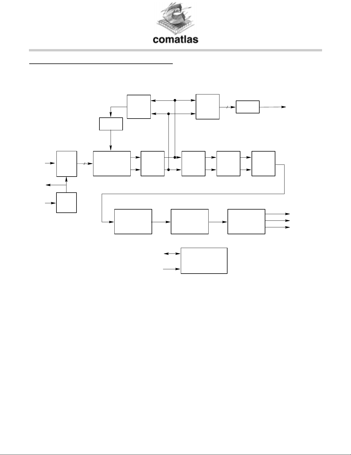
FIGURE 1 : FUNCTIONAL BLOCK DIAGRAM
IF
SACLK
XIN
ADC
PLL
9
NCO
BASE-BAND
CONVERSION
DE-INTERLEAVER
CLOCK
RECOVERY
FILTERS
BANK
SDA
SCL
EQUALIZER
R. S.
DECODER
INTERFACE
AGC TO AGC
8
CARRIER
RECOVERY
PWM
OUTPUT
INTERFACE
DO
DE-SCRAMBLER
OCLK
DEN
2
IC
comatlas reserves the right to make any change at anytime without notice. VES 1820X rev 2.0 / Mar 99 / p3
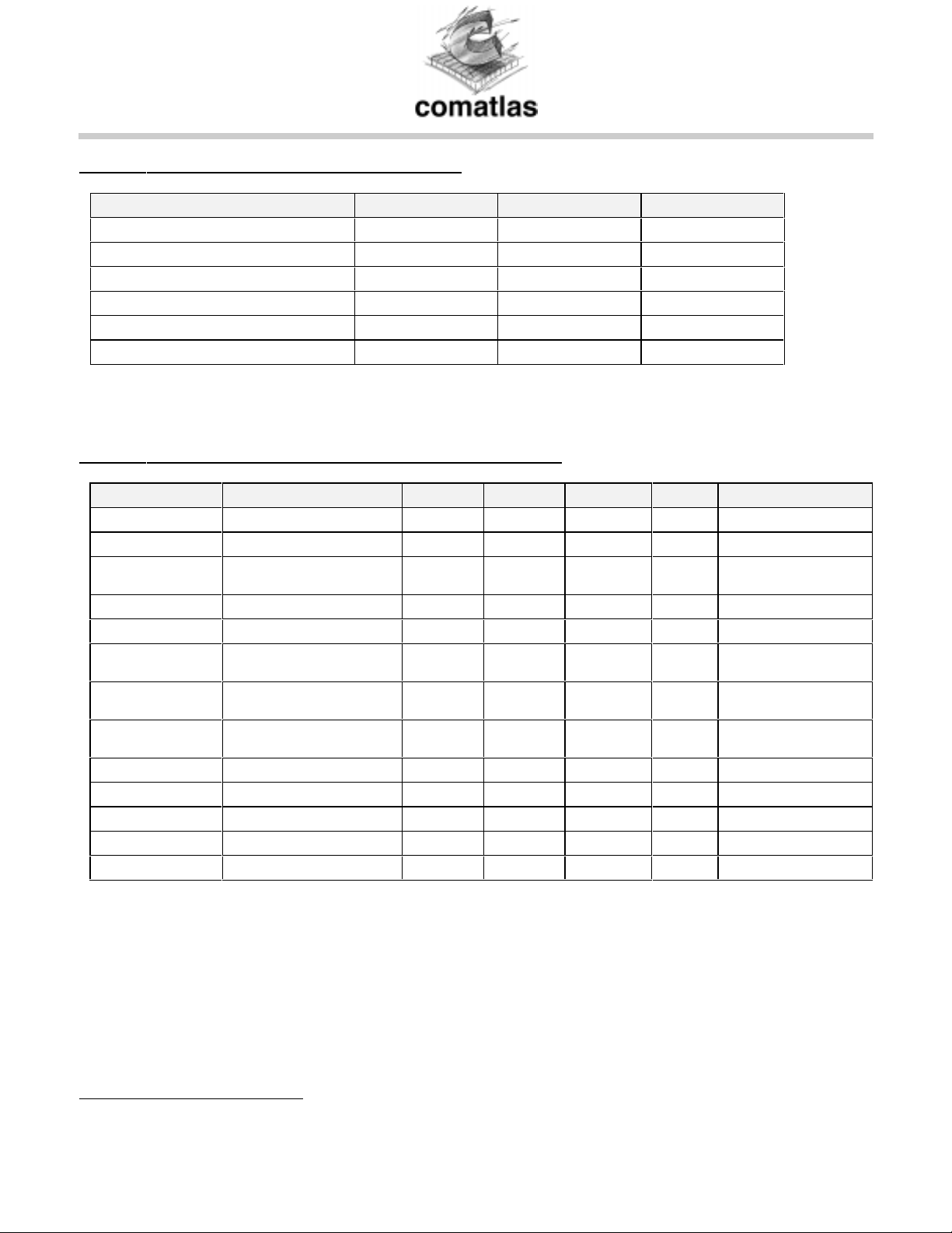
TABLE 1 : ABSOLUTE MAXIMUM RATINGS
Parameter Min Max Unit
Ambient operating temperature : Ta 0 70 °C
DC supply voltage - 0.5 + 4.1 V
DC Input voltage - 0.5 VDD + 0.5 V
DC Input Current ± 20 mA
Lead Temperature +300 °C
Junction Temperature +150 °C
Stresses above the absolute maximum ratings may cause permanent damage to the device. Exposure to absolute
maximum ratings conditions for extended periods may affect device reliability.
TABLE 2 : RECOMMENDED OPERATING CONDITIONS
Symbol Parameter Min Typ Max Unit Notes
VDD Digital supply voltage 3.14 3.3 3.46 V 3.3V ±5%
VCC 5V supply 4.75 5 5.25 V pin 17
Ta Operating temperature 0 70 °C Ambient
1
VIH
High-level input voltage 2 VCC + 0.3 V TTL input
VIL Low-level input voltage -0.5 0.8 V TTL input
2
VOH
VOL
2
High-level output
voltage
VDD -0.1
2.4
Low-level output voltage 0.1
V @ IOH = -0.8 mA
V @ IOL = 0.8 mA
0.4
IDD Supply current 200 mA @XIN = 57.84Mhz
CIN Input capacitance 15 pF
COUT Output capacitance 15 pF
VD2, VD3, VD4 Analog supply voltage 3.14 3.3 3.46 V 3.3V ± 5%
VIP Positive analog input 0.5 V
VIM Negative analog input -0.5 V
temperature
@ IOH = + 2mA
@ IOL = + 2mA
Symbol Rate =6Mbd
1
All inputs are 5V tolerant
2
IOH, IOL = ± 4mA only for pins SACLK, OCLK, SDA, CTRL1, CTRL2, IT
comatlas reserves the right to make any change at anytime without notice. VES 1820X rev 2.0 / Mar 99 / p4
 Loading...