

Philips UMA1022M Datasheet

INTEGRATED CIRCUITS
DATA SH EET
UMA1022M
Low cost dual frequency
synthesizer for radio telephones
Product specification
Supersedes data of 1998 May 15
File under Integrated Circuits, IC17
1998 Dec 09
Philips Semiconductors Product specification
Low cost dual frequency synthesizer for
radio telephones
FEATURES
• Low phase noise
• Low current from 3 V supply
• Fully programmable dividers
• 3-line serial interface bus
• Input reference buffer configurable as an oscillator with
external crystal resonator
• Wide compliance voltage charge pump outputs
• Two power-down input control pins.
APPLICATIONS
• 900 MHz and 2 GHz digital radio telephones
• Portable battery-powered radio equipment.
GENERAL DESCRIPTION
The UMA1022M BICMOS device integrates prescalers,
programmable dividers, a crystal oscillator/buffer and
phase comparators to implement two phase-locked loops.
The device is designed to operate from 3 NiCd or a single
LiIon cell in pocket phones, or from an external 3 V supply.
UMA1022M
The synthesizers operate at RF input frequencies up to
2.1 GHz and 550 MHz. All divider ratios are supplied via a
3-wire serial programming bus. The reference divider uses
a common, fully programmable part and a separate
subdivider section. In this way the comparison frequencies
are related to each other allowing optimum isolation
between charge pump pulses.
Separate power and ground pins are provided to the
analog (charge pump, prescaler) and digital (CMOS)
circuits. An independent supply for the crystal oscillator
section allows maximum frequency stability. The ground
leads should be externally short-circuited to prevent large
currents flowing across the die and thus causing damage.
and V
V
DD
V
must be equal to each other and equal to or greater
CCB
than VDD (e.g. VDD= 3 V and V
control voltage range).
The charge pump currents (phase detector gain) are fixed
by internal resistances and controlled by the serial
interface. Only passive loop filters are necessary;
the charge pumps function within a wide voltage
compliance range to improve the overall system
performance.
Suitable pin layout is chosen to minimize coupling and
interference between signals entering or leaving the chip.
must be at the same potential. V
DDX
= 5.5 V for wider VCO
CCA
CCA
and
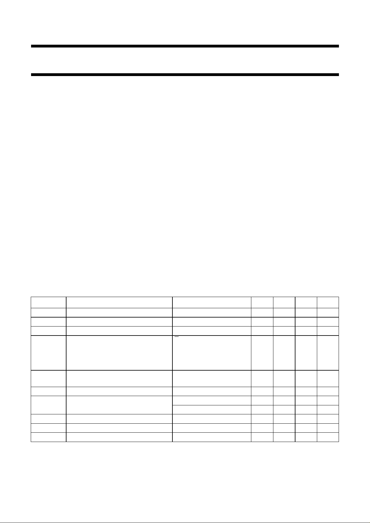
QUICK REFERENCE DATA
SYMBOL PARAMETER CONDITIONS MIN. TYP. MAX. UNIT
V
V
V
I
DD
CCA
DDX
tot
, V
digital supply voltage V
analog supply voltages V
CCB
crystal reference supply voltage V
all supply currents
(IDD+I
CCA+ICCB+IDDX
) in active
mode
CCA=VCCB
CCA=VCCB
DDX=VDD
E = 1; V
V
DDX=VDD
≥ V
DD
≥ V
DD
CCA=VCCB
= 3.0 V
= 3.0 V;
2.7 3.0 5.5 V
2.7 3.0 5.5 V
2.7 3.0 5.5 V
XON=0 − 14.65 − mA
XON=1 − 15.9 − mA
I
tot(pd)
total supply currents in power-down
− 40 −µA
mode
f
RF
f
IF
RF input frequency 300 − 2100 MHz
IF input frequency V
CCA=VCCB
≤ 4.0 V 50 − 550 MHz
50 − 400 MHz
f
xtal
f
PCmax
T
amb
crystal reference oscillator frequency 3 − 20 MHz
maximum loop comparison frequency − 2000 − kHz
operating ambient temperature −30 − +85 °C
1998 Dec 09 2
Philips Semiconductors Product specification
Low cost dual frequency synthesizer for
UMA1022M
radio telephones
ORDERING INFORMATION
TYPE NUMBER
NAME DESCRIPTION VERSION
UMA1022M SSOP20 plastic shrink small outline package; 20 leads; body width 4.4 mm SOT266-1
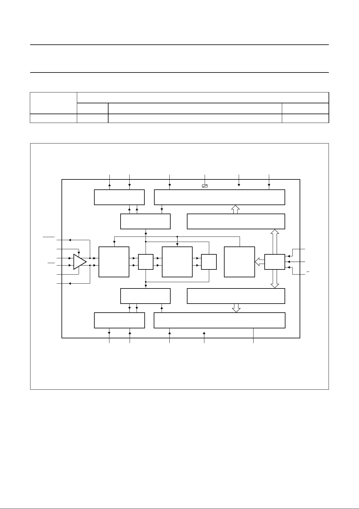
BLOCK DIAGRAM
handbook, full pagewidth
UMA1022M
V
CP
RF CHARGE PUMP
CCA
A
17 16 15
RF PHASE DETECTOR
RF
PACKAGE
A
AGND
14
RF PRESCALER AND DIVIDER
ON
A
13
RF DIVIDER LATCH
V
DD
12
XOUT
V
DDX
XIN
XIN
XGND
XOUT
18
19
20
1
2
3
COMMON
REFERENCE
DIVIDER
IF PHASE DETECTOR
IF CHARGE PUMP
45 67 8
CP
V
B
CCB
REFERENCE
SUBDIVIDER
IF
B
MUXMUX
IF PRESCALER AND DIVIDER
ON
B
REFERENCE
DIVIDER
LATCH
IF DIVIDER LATCH
DGND
SERIAL
BUS
11
CLK
10
DATA
9
E
MGE627
Fig.1 Block diagram.
1998 Dec 09 3
Philips Semiconductors Product specification
Low cost dual frequency synthesizer for
radio telephones
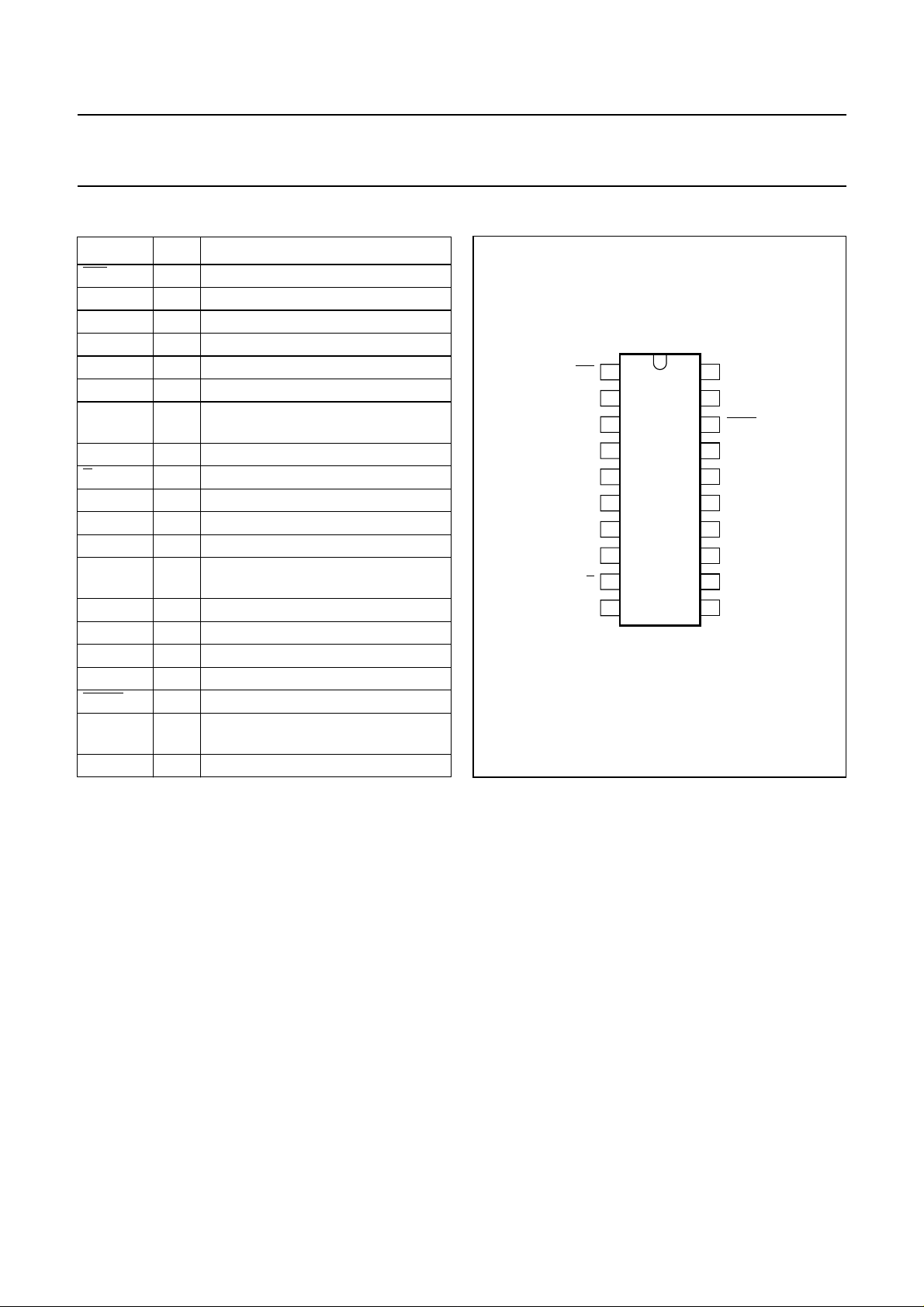
PINNING
SYMBOL PIN DESCRIPTION
XIN 1 inverting crystal reference input
XGND 2 ground for crystal oscillator circuits
XOUT 3 crystal oscillator buffer output
CP
B
V
CCB
IF
B
ON
B
DGND 8 digital circuits ground
E 9 programming bus enable input
DATA 10 programming bus data input
CLK 11 programming bus clock input
V
DD
ON
A
AGND 14 analog circuits ground
RF
A
V
CCA
CP
A
XOUT 18 inverting oscillator buffer output
V
DDX
XIN 20 non-inverting crystal reference input
4 IF synthesizer charge pump output
5 analog supply to IF synthesizer
6 IF VCO main divider input
7 IF power-on input; ONB= HIGH
means IF synthesizer is active
12 digital circuits supply voltage
13 RF power-on input; ONA= HIGH
means RF synthesizer is active
15 RF VCO main divider input
16 analog supply to RF synthesizer
17 RF synthesizer charge pump output
19 supply voltage to crystal oscillator
circuits
handbook, halfpage
1
XIN
XGND
2
3
XOUT
4
CP
B
5
V
CCB
IF
ON
DGND
DATA
B
B
E
10
UMA1022M
6
7
8
9
MGE626
Fig.2 Pin configuration.
UMA1022M
XIN
20
19
V
DDX
18
XOUT
CP
17
A
16
V
CCA
15
RF
A
AGND
14
ON
13
A
12
V
DD
CLK
11
1998 Dec 09 4

Philips Semiconductors Product specification
Low cost dual frequency synthesizer for
radio telephones
FUNCTIONAL DESCRIPTION
Main dividers
The main dividers are clocked at pin RF
oscillator signal and at pin IFB by the IF oscillator signal.
The inputs are AC coupled through external capacitors.
Input impedances are high, dominated by parasitic
package capacitances, so matching is off-chip.
The sensitive dividers operate with signal levels from
35 to 225 mV (RMS), at frequencies up to 2.1 GHz
(RF part) and up to 550 MHz (IF part). Both include
programmable bipolar prescalers followed by CMOS
counters. The RF main divider allows programmable ratios
from 512 to 65535; the IF blocks accept values between
128 and 16383.
Crystal oscillator
A fully differential low-noise amplifier/buffer is integrated
providing outputs to drive other circuits, and to build a
crystal oscillator; only needed are an external resonance
circuit and tuning elements (temperature compensation).
A bus controlled power-down mode disables the low-noise
amplifier to reduce current if not needed.
The normal differential input pins drive a clock buffer to
provide edges to the programmable reference divider at
frequencies up to 20 MHz. The inputs are AC coupled
through external capacitors, and operate with signals
down to 35 mV (RMS) and up to 0.5 V (RMS).
Various crystal oscillator structures can be built using the
amplifier. By coupling one output back to the appropriate
input through the resonator, and decoupling the other input
to ground, the second output becomes available to deliver
the reference frequency to other circuits.
Reference dividers
A first common divider circuit produces an output
frequency for RF or IF synthesizer phase comparison,
depending on the P/A bit. It drives a second independent
divider, which delivers the reference edge to the IF or RF
synthesizer phase comparator. When P/A is logic 1, the
output of the subdivider is connected to the RF phase
comparator, whereas the output of the common divider is
connected to the IF phase detector.
by the RF
A
UMA1022M
Phase comparators
The phase detectors are driven by the output edges
selected by the main and reference dividers. Each
generates lead and lag signals to control the appropriate
charge pump. The pumps output current pulses appear at
pins CP
The current pulse duration is at least equal to the
difference in time of arrival of the edges from the two
dividers. If the main divider edge arrives first, CPA or CP
sink current. If the reference divider edge arrives first, CP
or CPB source current. For correct PLL operation the
VCOs need to have a positive frequency/voltage control
slope.
The currents at CPA and CPB are programmed via the
serial bus as multiples of an internally-set reference
current. The passage into power-down mode is
synchronized with respect to the phase detector to prevent
output current pulses being interrupted. Additional circuitry
is included to ensure that the gain of the phase
comparators remains linear even for small phase errors.
Serial programming bus
A simple 3-line unidirectional serial bus is used to program
the circuit. The 3 lines are DATA, clock (CLK) and enable
(
E). The data sent to the device is loaded in bursts framed
byE. Programming clock edges and their appropriate data
bits are ignored untilE goes active LOW. The programmed
information is loaded into the addressed latch when E
returns HIGH. During normal operation, E should be kept
HIGH. Only the last 19 bits serially clocked into the device
are retained within the programming register.
Additional leading bits are ignored, and no check is made
on the number of clock pulses. The NMOS-rich design
uses virtually no current when the bus is inactive;
power-up is initiated when enable is taken LOW, and
power-down occurs a short time after enable returns
HIGH. Bus activity is allowed when either synthesizer is
active or in power-down (ONA and ONB inputs LOW)
mode. Fully static CMOS registers retain programmed
data whatever the power-down state, as long as the supply
voltage is present.
(RF synthesizer) and CPB (IF synthesizer).
A
B
A
The phase comparators run at related frequencies with a
controlled phase difference to avoid interference when
in-lock. The common 10-bit section permits divide ratios
from 8 to 1023; the second subdivider allows phase
comparison frequency ratios between 1 and 16. Table 2
indicates how to program the corresponding bits to get the
wanted ratio.
1998 Dec 09 5
Philips Semiconductors Product specification
Low cost dual frequency synthesizer for
radio telephones
Data format
The leading bits (dt15 to dt0) make up the data field, while
the trailing three bits (ad2 to ad0) comprise an address
field. The UMA1022M uses 4 of the 8 available addresses.
The data format is shown in Table 1. The first bit entered
is dt15, the last bit is ad0. For the divider ratios, the first
bits entered (P0 and R0) are the Least Significant Bits
(LSB). This is different from previous Philips
synthesizers.
The trailing address bits are decoded on the rising edge of
E. This produces an internal load pulse to store the data in
the addressed latch. To avoid erroneous divider ratios, the
load pulse is not allowed during data reads by the
frequency dividers. This condition is guaranteed by
respecting a minimum E pulse width after data
transfer.The test register bits should not normally be
programmed active (HIGH); normal operation requires
them set LOW. When the supply voltage is established an
internal power-up initialization pulse is generated to
preconfigure the circuit state. Production testing does not
verify that all bits are preconfigured correctly.
UMA1022M
Power-down mode
The RF and IF synthesizers are on when respectively the
input signal ON
dividers and phase detector are synchronized to avoid
random phase errors. When turnedoff, the phase detector
is synchronized to avoid interrupting charge pump pulses.
The UMA1022M has a very low current consumption in the
power-down mode.
and ONB are HIGH. When turned on, the
A
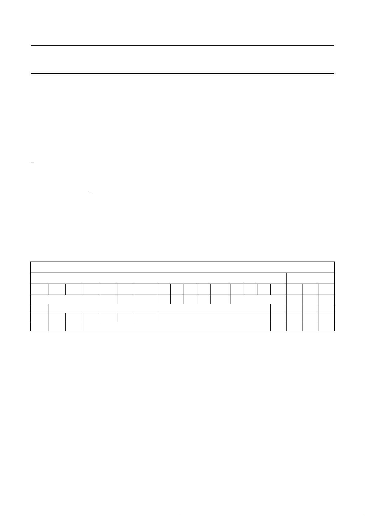
Table 1 Bit allocation; note 1
FIRST IN REGISTER BIT ALLOCATION LAST IN
DATA FIELD ADDRESS
dt15 dt14 dt13 dt12 dt11 dt10 dt9 dt8 dt7 dt6 dt5 dt4 dt3 dt2 dt1 dt0 ad2 ad1 ad0
P0
(6)
Test bits
(2)
CPI S/D XON
RF synthesizer main divider coefficient P15 0 0 0
XXXXXXR0
XXA0
(6)
IF synthesizer main divider coefficient A13 0 1 0
(3)
XXXXP/A
(6)
reference divider coefficient R9 0 0 1
(4)
REFDIV2
(5)
011
Notes
1. X = don’t care.
2. The test bits (at address 011) should not be programmed with any other value except all zeros for normal operation.
3. Bit XON = power-on of crystal oscillator low-noise amplifier; logic 1 turns on circuit block.
4. Bit P/A = 1 selects the output of the reference subdivider to the RF synthesizer and the output of the common
reference divider to the IF synthesizer.
5. The coefficient REFDIV2 (4 bits) selects the phase comparison ratio (1 to 16) between IF and RF synthesizers
(see Table 2).
6. P0 is the LSB of the RF main divider coefficient; R0 is the LSB of the reference divider coefficient; A0 is the LSB of
the IF main divider.
1998 Dec 09 6
 Loading...