

Philips UMA1020M Datasheet

INTEGRATED CIRCUITS
DATA SH EET
UMA1020M
Low-voltage dual frequency
synthesizer for radio telephones
Product specification
Supersedes data of November 1994
File under Integrated Circuits, IC03
1995 Jun 15
Philips Semiconductors Product specification
Low-voltage dual frequency
synthesizer for radio telephones
FEATURES
• Low current from 3 V supply
• Fully programmable RF divider
• 3-line serial interface bus
• Second synthesizer to control first IF or offset loop
frequency
• Independent fully programmable reference dividers for
each loop, driven from external crystal oscillator
• Dual phase detector outputs to allow fast frequency
switching
• Integrated digital-to-analog converter
• Dual power-down modes.
APPLICATIONS
• 2 GHz mobile telephones
• Portable battery-powered radio equipment.
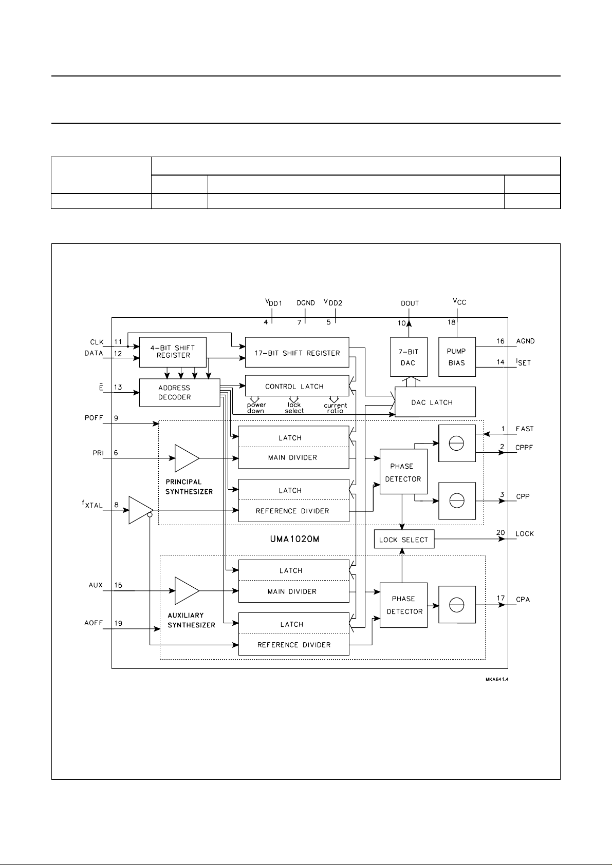
GENERAL DESCRIPTION
The UMA1020M BICMOS device integrates prescalers,
programmable dividers, and phase comparators to
implement two phase-locked loops. The device is
designed to operate from 3 NiCd cells, in pocket phones,
with low current and nominal 5 V supplies.
UMA1020M
The principal synthesizer operates at RF input frequencies
up to 2.4 GHz the auxiliary synthesizer operates at
300 MHz. The auxiliary loop is intended for the first IF or to
transmit offset loop-frequency settings. Each synthesizer
has a fully programmable reference divider. All divider
ratios are supplied via a 3-wire serial programming bus.
Separate power and ground pins are provided to the
analog and digital circuits. The ground leads should be
externally short-circuited to prevent large currents flowing
across the die and thus causing damage. Digital supplies
and V
V
DD1
must be equal to or greater than VDD (i.e. VDD= 3 V and
VCC= 5 V for wider tuning range).
The principal synthesizer phase detector uses two charge
pumps, one provides normal loop feedback, while the
other is only active during fast mode to speed-up
switching. The auxiliary loop has a separate phase
detector. All charge pump currents (gain) are fixed by an
external resistance at pin I
filters are used; the charge-pumps function within a wide
voltage compliance range to improve the overall system
performance. An on-chip 7-bit DAC enables adjustment of
an external function, such as the temperature
compensation of a crystal oscillator.
must also be at the same potential. V
DD2
(pin 14). Only passive loop
SET
CC
QUICK REFERENCE DATA
SYMBOL PARAMETER CONDITIONS MIN. TYP. MAX. UNIT
, V
V
CC
I
CC+IDD
DD
supply voltage VCC≥ V
DD
principal synthesizer supply current auxiliary synthesizer in
2.7 − 5.5 V
− 9.4 − mA
power-down mode
I
, I
CCPD
f
VCO
f
AI
f
XTAL
f
PPC
f
APC
T
amb
principal and auxiliary synthesizer
supply current
current in power-down mode per supply − 12 −µA
DDPD
principal input frequency 1700 − 2400 MHz
auxiliary input frequency 20 − 300 MHz
crystal reference input frequency 3 − 40 MHz
principal phase comparator frequency − 200 − kHz
auxiliary phase comparator frequency − 200 − kHz
operating ambient temperature −30 − +85 °C
principal and auxiliary
synthesizers ON
− 12.1 − mA
1995 Jun 15 2
Philips Semiconductors Product specification
Low-voltage dual frequency
UMA1020M
synthesizer for radio telephones
ORDERING INFORMATION
TYPE NUMBER
NAME DESCRIPTION VERSION
UMA1020M SSOP20 plastic shrink small outline package; 20 leads; body width 4.4 mm SOT266-1
BLOCK DIAGRAM
PACKAGE
Fig.1 Block diagram.
1995 Jun 15 3
Philips Semiconductors Product specification
Low-voltage dual frequency
synthesizer for radio telephones
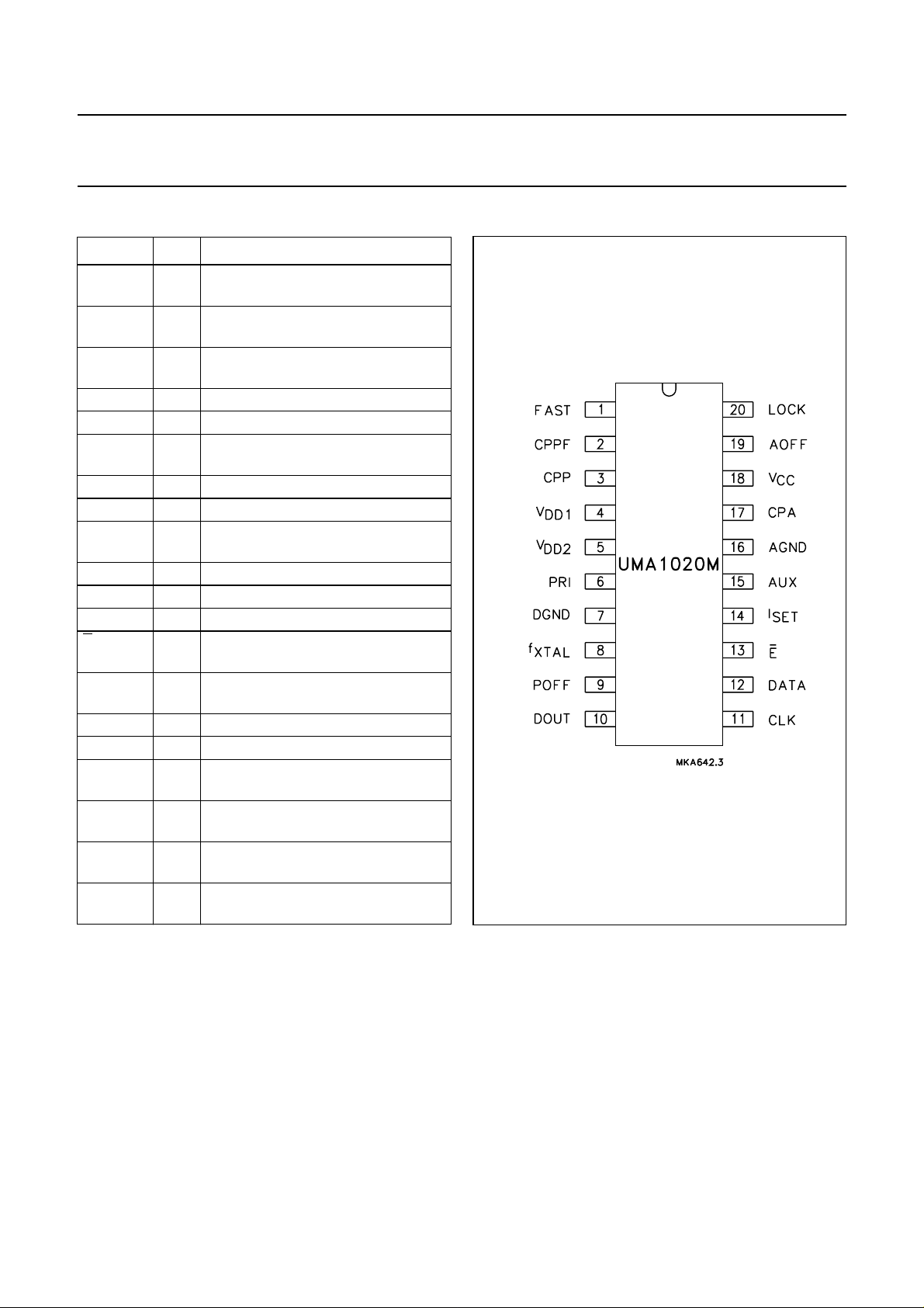
PINNING
SYMBOL PIN DESCRIPTION
FAST 1 control input to speed-up main
synthesizer
CPPF 2 principal synthesizer speed-up
charge-pump output
CPP 3 principal synthesizer normal
charge-pump output
V
DD1
V
DD2
PRI 6 2 GHz principal synthesizer
DGND 7 digital ground
f
XTAL
POFF 9 principal synthesizer power-down
DOUT 10 7-bit digital-to-analog output
CLK 11 programming bus clock input
DATA 12 programming bus data input
E 13 programming bus enable input
I
SET
AUX 15 auxiliary synthesizer frequency input
AGND 16 analog ground
CPA 17 auxiliary synthesizer charge-pump
V
CC
AOFF 19 auxiliary synthesizer power-down
LOCK 20 in-lock detect output (main PLL); test
4 digital power supply 1
5 digital power supply 2
frequency input
8 crystal frequency input from TCXO
input
(active LOW)
14 regulator pin to set the charge-pump
currents
output
18 supply for charge-pump and DAC
circuits
input
mode output
UMA1020M
Fig.2 Pin configuration.
FUNCTIONAL DESCRIPTION
Principal synthesizer
Programmable reference and main dividers drive the
principal PLL phase detector. Two charge pumps produce
phase error current pulses for integration in an external
loop filter. A hardwired power-down input POFF (pin 9)
ensures that the dividers and phase comparator circuits
can be disabled.
1995 Jun 15 4
The PRI input (pin 6) drives a preamplifier to provide the
clock to the first divider stage. The preamplifier has a high
input impedance, dominated by pin and pad capacitance.
The circuit operates with signal levels from 60 mV to
180 mV (RMS), and at frequencies up to 2.4 GHz. The
high frequency divider circuits use bipolar transistors,
slower bits are CMOS. Divide ratios (512 to 131071) allow
a 2 MHz phase comparison frequency.

Philips Semiconductors Product specification
Low-voltage dual frequency
synthesizer for radio telephones
The reference and main divider outputs are connected to
a phase/frequency detector that controls two charge
pumps. The two pumps have a common bias setting
current that is set by an external resistance. The ratio
between currents in fast and normal operating modes can
be programmed via the 3-wire serial bus. The low current
pump remains active except in power-down. The high
current pump is enabled via the control input FAST (pin 1).
By appropriate connection to the loop filter, dual bandwidth
loops are provided: short time constant during frequency
switching (FAST mode) to speed-up channel changes and
low bandwidth in the settled state (on-frequency) to reduce
noise and breakthrough levels.
The principal synthesizer speed-up charge pump (CPPF)
is controlled by the FAST input in synchronization with
phase detector operation in such a way that potential
disturbances are minimized. The dead zone (caused by
finite time taken to switch the current sources on or off) is
cancelled by feedback from the normal pump output to the
phase detector thereby improving linearity.
An open drain transistor drives the output pin LOCK
(pin 20). It is recommended that the pull-up resistor from
this pin to VDD is chosen such that the value is high enough
to keep the sink current in the LOW state below 400 µA.
The circuit can be programmed to output either the phase
error in the principal or auxiliary phase detectors or the
combination from both detectors (OR function). The
resultant output will be a current pulse with the duration of
the selected phase error. By appropriate external filtering
and threshold comparison, an out-of-lock or an in-lock flag
is generated.
Auxiliary synthesizer
The auxiliary synthesizer has a 14-bit main divider and an
11-bit reference divider. A separate power-down input
AOFF (pin 19), disables currents in the auxiliary dividers,
phase detector, and charge pump. The auxiliary input
signal is amplified and fed to the main divider. The input
buffer presents a high impedance, dominated by pin and
pad capacitance. First divider stages use bipolar
technology operating at input frequencies up to 300 MHz;
the slower bits are CMOS. The auxiliary loop phase
detector and charge pump use similar circuits to the main
loop low-current phase comparator, including dead-zone
compensation feedback.
UMA1020M
Serial programming bus
A simple 3-line unidirectional serial bus is used to program
the circuit. The 3 lines are DATA, CLK and
data sent to the device is loaded in bursts framed by E.
Programming clock edges and their appropriate data bits
are ignored until E goes active LOW. The programmed
information is loaded into the addressed latch when E
returns inactive HIGH. Only the last 21 bits serially clocked
into the device are retained within the programming
register. Additional leading bits are ignored, and no check
is made on the number of clock pulses. The fully static
CMOS design uses virtually no current when the bus is
inactive. It can always capture new programmed data
even during power-down of main and auxiliary loops.
However when either principal synthesizer or auxiliary
synthesizer or both are powered-on, the presence of a
TCXO signal is required at pin 8 (f
programming.
Data format
Data is entered with the most significant bit first. The
leading bits make up the data field, while the trailing four
bits are an address field. The UMA1020M uses 6 of the
16 available addresses. The data format is shown in
Table 1. The first entered bit is p1, the last bit is p21.
The trailing address bits are decoded on the inactive edge
E. This produces an internal load pulse to store the data
of
in one of the addressed latches. To ensure that the data is
correctly loaded on first power-up, E should be held LOW
and only taken HIGH after having programmed an
appropriate register. To avoid erroneous divider ratios, the
pulse is not allowed during data reads by the frequency
dividers. This condition is guaranteed by respecting a
minimum E pulse width after data transfer. The
corresponding relationship between data fields and
addresses is given in Table 2.
XTAL
E (enable). The
) for correct
The auxiliary reference divider is clocked on the opposite
edge of the principal reference divider to ensure that active
edges arrive at the auxiliary and principal phase detectors
at different times. This minimizes the potential for
interference between the charge pumps of each loop.
1995 Jun 15 5
1995 Jun 15 6
Table 1 Format of programmed data
LAST IN PROGRAMMING REGISTER BIT USAGE FIRST IN
p21 p20 p19 p18 p17 p16 ../.. p2 p1
ADD0 ADD1 ADD2 ADD3 DATA0 DATA1 ../.. DATA15 DATA16
LATCH ADDRESS LSB DATA COEFFICIENT MSB
Table 2 Bit allocation (note 1)
FT REGISTER BIT ALLOCATION LT
p1 p2 p3 p4 p5 p6 p7 p8 p9 p10 p11 p12 p13 p14 p15 p16 p17 p18 p19 p20 p21
dt16 dt15 dt14 dt13 dt12 DATA FIELD dt4 dt3 dt2 dt1 dt0 ADDRESS
TEST BITS
X X X X OLP OLA CR1 CR0 X X sPOFF sAOFF X X X X X 0 0 0 1
PM16 PRINCIPAL MAIN DIVIDER COEFFICIENT PM0 0 1 0 0
X X X X X X PR10 PRINCIPAL REFERENCE DIVIDER COEFFICIENT PR0 0 1 0 1
X X X AM13 AUXILIARY MAIN DIVIDER COEFFICIENT AM0 0 1 1 0
X X X X X X AR10 AUXILIARY REFERENCE DIVIDER COEFFICIENT AR0 0 1 1 1
X X X X X X X X X 0 DA6 7-BIT DAC DA0 1 0 0 0
Notes
1. FT = first; LT = last; sPOFF = software power-down for principal synthesizer (1 = OFF); sAOFF = software power-down for auxiliary synthesizer
(1 = OFF).
2. The test register should not be programmed with any other value except all zeros for normal operation.
(2)
0000
Philips Semiconductors Product specification
Low-voltage dual frequency
synthesizer for radio telephones
Table 3 Out-of-lock select
OLP OLA OUT-OF-LOCK ON PIN 20
0 0 output disabled
0 1 auxiliary phase error
1 0 principal phase error
1 1 both auxiliary and principal
UMA1020M
 Loading...