

Philips UMA1016AT, UMA1016xT, UMA1016BT Datasheet

DATA SH EET
Product specification
Supersedes data of June 1992
File under Integrated Circuits, IC03
1995 Jul 12
INTEGRATED CIRCUITS
UMA1016xT
Frequency synthesizer for
radio communication equipment
1995 Jul 12 2
Philips Semiconductors Product specification
Frequency synthesizer for
radio communication equipment
UMA1016xT
FEATURES
• RF input frequencies to 1 GHz
• Fully programmable RF divider
• 3-wire serial bus interface
• On-chip 3 to 16 MHz crystal oscillator
• Mask programmable ÷2to÷31 reference divider ratio
• Up to 1 MHz channel spacing
• Crystal frequency buffered output
• Dual register architecture for fast Tx/Rx switching in
TDD single synthesizer systems
• Phase detector compensated for supply and
temperature variations
• Power-down mode.
APPLICATIONS
• 900 MHz cordless telephones
• Portable battery-powered radio equipment.
GENERAL DESCRIPTION
The UMA1016xT is a low power synthesizer for radio
communications. Manufactured in bipolar technology, it is
designed for a 70 to 1000 kHz channel spacing in the
500 to 1000 MHz band. The channel is programmed via a
3-wire serial bus. The internal dual register architecture
allows a single synthesizer to be used in TDD systems.
Fast switching between transmit and receive frequencies
is achieved without the need for bus overhead. It also
incorporates a sensitive, low power RF divider and a
dead-zone-eliminated 3-state phase comparator.
A power-down mode enables the circuit to be idled.
QUICK REFERENCE DATA
ORDERING INFORMATION
Notes
1. UMA1016AT has a Reference Division Factor of 27.
2. UMA1016AT has a Reference Division Factor of 16.
3. UMA1016xT is a customized version.
SYMBOL PARAMETER CONDITIONS MIN. TYP. MAX. UNIT
Supply
V
CC
supply voltage 4.5 − 5.5 V
V
DD
supply voltage 4.5 − 5.5 V
I
CC
+ I
DD
supply current − 12 − mA
I
DD(pd)
digital supply current in power-down − 0.8 − mA
f
ref
phase comparator frequency 70 250 1000 kHz
RF
I
RF input frequency T
amb
= −10 to +70°C 500 − 800 MHz
T
amb
= 0 to +70°C 500 − 1000 MHz
T
amb
operating ambient temperature −10 − +70 °C
TYPE
NUMBER
PACKAGE
NAME PIN POSITION VERSION
UMA1016AT
(1)
SO16 plastic small outline package; 16 leads; body width 3.9 mm SOT109-1
UMA1016BT
(2)
SO16 plastic small outline package; 16 leads; body width 3.9 mm SOT109-1
UMA1016xT
(3)
SO16 plastic small outline package; 16 leads; body width 3.9 mm SOT109-1
1995 Jul 12 3
Philips Semiconductors Product specification
Frequency synthesizer for
radio communication equipment
UMA1016xT
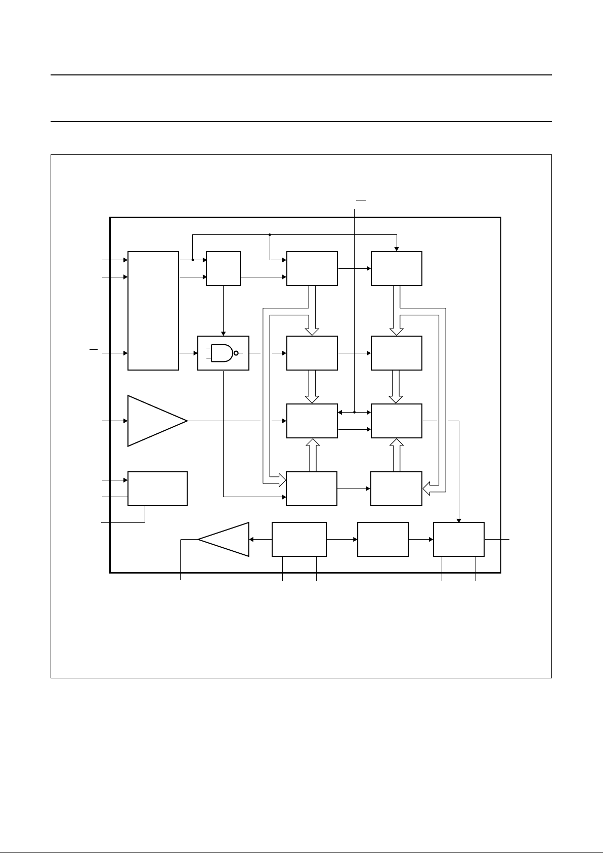
BLOCK DIAGRAM
Fig.1 Block diagram.
handbook, full pagewidth
MGA193 - 1
REGISTER
Tx
LATCH
RF
DIVIDER
Rx
LATCH
OSCILLATOR
BIAS
GENERATORS
PHASE
DETECTOR
INTERFACE
Ck
DQ
AMPLIFIER
BUFFER
DIVIDER
2 – 31
.
.
REGISTER
Tx
LATCH
MAIN
DIVIDER
Rx
LATCH
12
3
4
5
6
7
16
15
14
12
11
10
9
CP
V
CC
AGND
Tx/Rx
EN
CK
DATA
RO1 RO2
V
DD
REFCK
HPDN
DGND
RFI
UMA1016XT
1995 Jul 12 4
Philips Semiconductors Product specification
Frequency synthesizer for
radio communication equipment
UMA1016xT
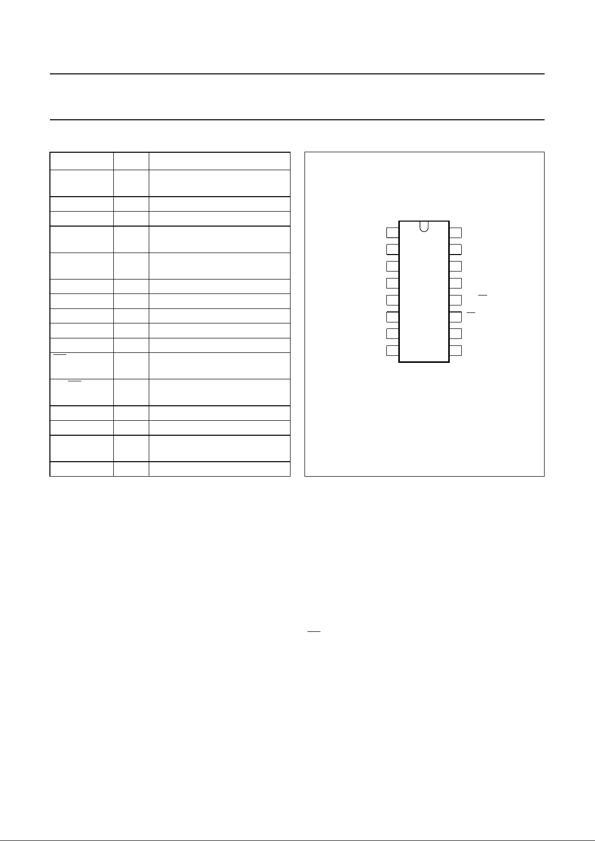
PINNING
SYMBOL PIN DESCRIPTION
RO1 1 crystal oscillator input or TCXO
input
RO2 2 oscillator output to crystal circuit
V
DD
3 5 V supply to digital section
REFCK 4 reference crystal frequency
buffered output
HPDN 5 Hardware Power-Down Not;
IC operates when pin is HIGH
DGND 6 digital ground
RFI 7 1 GHz RF signal input
i.c. 8 internally connected
DATA 9 programming bus data input
CK 10 programming bus clock input
EN 11 programming bus enable input
(active LOW)
TX/
RX 12 transmit (HIGH)/receive (LOW)
mode select input
i.c. 13 internally connected
AGND 14 analog ground
V
CC
15 5 V supply to charge pump
circuit
CP 16 charge pump output
Fig.2 Pin configuration.
handbook, halfpage
1
2
3
4
5
6
7
8
16
15
14
13
12
11
10
9
CP
V
CC
AGND
i.c.
TX/RX
EN
CK
DATA
RO1
RO2
V
DD
REFCK
HPDN
DGND
RFI
i.c.
UMA1016XT
MGA192 - 1
FUNCTIONAL DESCRIPTION
General
The UMA1016xT is a low power synthesizer for radio
communications in the range 500 to 1000 MHz. It includes
an oscillator circuit, reference divider, RF divider, 3-state
phase and frequency comparator, charge pump and main
control circuit for the transfer of serial data into two internal
registers.
V
DD
supplies power to the digital circuits while VCC powers
the charge pump. VDD and VCC are nominally 5 V but will
operate in the range 4.5 V to 5.5 V.
Reduced noise coupling is facilitated by separate digital
and analog ground pins which must always be externally
connected to the same DC potential to prevent the flow of
large currents across the die.
The synthesizer is placed in idle mode during power-down
but the oscillator and buffer remain operative and may be
used as a clock for system timing.
Main divider
The main divider is a fully programmable pulse-swallow
type. Following a sensitive (50 mV, −13 dBm) input
amplifier, the RF signal is applied to a 13-bit divider
(MD13 to MD1). The division ratio is provided via the serial
bus to two 13-bit latches, corresponding to transmit and
receive frequencies. The serial programming register is
written to under processor control, independently of divider
operation. This removes difficulty if using a low data bus
transmission speed. The new ratio is transferred to the
appropriate latch when the programming enable signal
(
EN) returns HIGH.
The last register bit (PB0) is used to determine whether the
new value is loaded into the transmit (PB0 = 1) or receive
(PB0 = 0) frequency latch. To avoid spurious phase
changes, the divider incorporates the new ratio only at the
end of the on-going reference period. The minimum
division ratio is 512. One reference cycle is required to
update a new ratio. Internal power-on occurs rapidly.

1995 Jul 12 5
Philips Semiconductors Product specification
Frequency synthesizer for
radio communication equipment
UMA1016xT
Oscillator
External capacitive feedback is applied to the common
collector Colpitts oscillator which has high voltage supply
rejection and negligible temperature drift. It is designed to
function as an input buffer without the need for external
components when a TCXO or other clock is used.
A separate output buffer, which remains active during
power-down (HPDN taken LOW), provides a TTL
compatible signal to drive external logic circuits (REFCK).
Reference divider
The reference divider has a fixed divider ratio set by metal
masking between 2 and 31. For example, a 4 MHz crystal
connected to the oscillator and a ÷16 ratio allows a
channel spacing of 250 kHz. Other frequencies and ratios
are possible.
Phase comparator
The phase comparator combines a phase and frequency
detector and charge pump (see Fig.3). The charge pump
current is internally fixed and determined for fast switching.
It is compensated against power supply and temperature
variation.
The detector is assembled from dual D-type flip-flops
which, together with feedback, remove the ‘dead’ zone.
Upon the detection of a phase error, either UP or DO go
HIGH. This gates the appropriate current generator to
source or sink 1.75 mA at the output pin. When no phase
error is detected, CP becomes 3-state. The tuning voltage
of the VCO is established from the sum of the current
pulses into the loop filter.
A simple passive loop filter may be used to offer high
performance without requiring an operational-amp.
The phase comparator function is summarized in Table 2.
Main control interface
The programming control interface permits access to two
internal latches, denoted Tx and Rx. The serial input bits
on DATA, entered MSB first, are converted to a parallel
word and stored in the appropriate latch under the control
of the last entered register bit (PB0). When this is set
HIGH, data serially fed to the register is loaded into the
transmit (Tx) latch; when PB0 is LOW, the data is
transferred to the receive latch (Rx).
The data sent to the synthesizer is loaded in bursts framed
by the signal
EN. Programming clock edges, together with
their appropriate data bits, are ignored until EN becomes
active (LOW). The internal latches are updated with the
latest programming data whenEN returns inactive (HIGH).
Only the last 15 bits serially clocked into the device are
retained within the programming register. One extra shift
register bit (PB7) can be internally added via metal
masking to allow direct software compatibility with a 7-bit
swallow counter and a 64/65 dual-modulus prescaler.
No check is made on the number of clock pulses received
during the time that programming is enabled. EN going
HIGH while CLOCK is still LOW generates an active clock
edge causing a shift of the data bits.
Data programmed into the register is lost during
power-down (HPDN taken LOW). The maximum serial bus
clock speed is specified as 5 MHz. Minimum speed is
limited by the clock edge rise and fall times to ensure that
no data transparency condition can exist.
Independent of any serial programming activity, the
RF divider chain uses the data previously stored within the
selected latch to determine the synthesized channel
frequency. The Tx/Rx signal controls which latch is read to
preload the counter bits at each division cycle. When new
data is updated into the device, it is used during the cycle
following latch selection by the Tx/Rx control line.
If the Tx/Rx line is tied LOW, only data loaded into the Rx
latch is used. In this event the serial data stream clocked
into the synthesizer must terminate with an ‘0’. The logic
diagram for the first bits of the programming interface is
shown in Fig.3. The other bits are processed in a similar
manner by a further 9 stages of the shift
register-latches-multiplexer.
The signals supplied to the circuit are described by the
timing diagram. The table of values has been specified for
maximum bus speed. Under slow clocking conditions, rise
and fall times must not be excessively slow.
 Loading...