

Philips UMA1015AM-C1 Datasheet

DATA SH EET
Product specification
Supersedes data of 1997 Jun 10
File under Integrated Circuits, IC17
1997 Sep 03
INTEGRATED CIRCUITS
UMA1015AM
Low-power dual frequency
synthesizer for radio
communications
1997 Sep 03 2
Philips Semiconductors Product specification
Low-power dual frequency synthesizer
for radio communications
UMA1015AM
FEATURES
• Two fully programmable RF dividers up to 1.1 GHz
• Fully programmable reference divider up to 35 MHz
• 2 : 1 or 1 : 1 ratio of selectable reference frequencies
• Fast three-line serial bus interface
• Adjustable phase comparator gain
• Programmable out-of-lock indication for both loops
• On-chip voltage doubler
• Low current consumption from 3 V supply
• Separate power-down mode for each synthesizer
• Up to 4 open-drain output ports
• Crystal input frequency signal inverted and buffered
output on separate pin.
APPLICATIONS
• Cordless telephone
• Hand-held mobile radio.
GENERAL DESCRIPTION
The UMA1015AM is a low-power dual frequency
synthesizer for radio communications which operates in
the 50 to 1100 MHz frequency range. Each synthesizer
consists of a fully programmable main divider, a phase and
frequency detector and a charge pump. There is a fully
programmable reference divider common to both
synthesizers which operates up to 35 MHz.
The device is programmed via a 3-wire serial bus which
operates up to 10 MHz. The charge pump currents (gains)
are fixed by an external resistance at pin 20 (I
SET
).
The BiCMOS device is designed to operate from 2.7 V
(3 NiCd cells) to 5.5 V at low current. Digital supplies V
DD1
and V
DD2
must be at the same potential. The charge pump
supply (VCC) can be provided by an external source or
on-chip voltage doubler. VCC must be equal to or higher
than V
DD1
.
Each synthesizer can be powered-down independently via
the serial bus to save current. It is also possible to
power-down the device via the HPD input (pin 5).
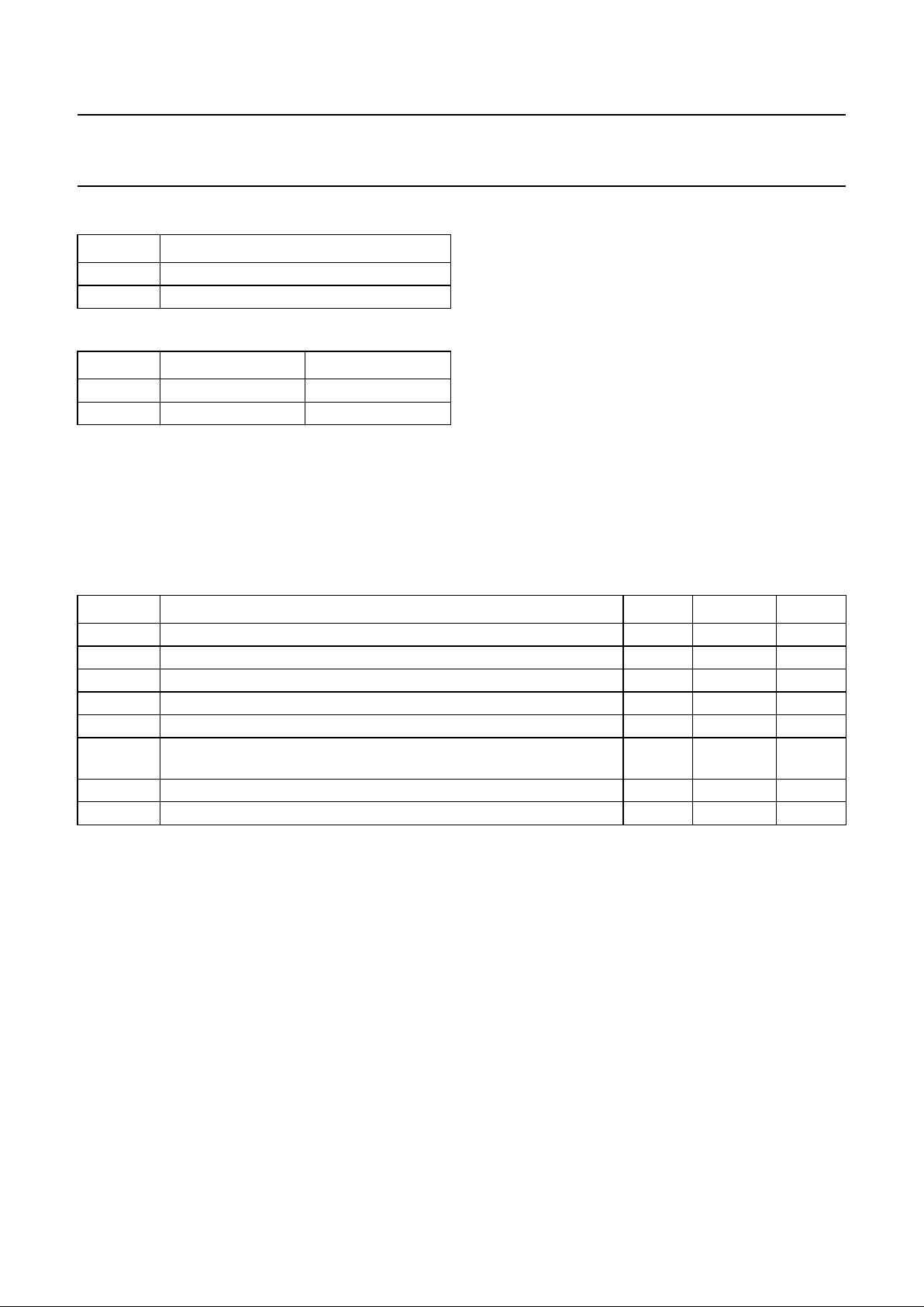
QUICK REFERENCE DATA
SYMBOL PARAMETER CONDITIONS MIN. TYP. MAX. UNIT
V
DD1
, V
DD2
digital supply voltage V
DD1=VDD2
2.7 − 5.5 V
V
CC
charge pump supply voltage external supply; doubler
disabled; VCC≥ V
DD
2.7 − 6.0 V
V
CCvd
charge pump supply from
voltage doubler
doubler enabled − 2V
DD1
− 0.6 6.0 V
I
DD1+IDD2+ICC
operating supply current both synthesizers ON; doubler
disabled; V
DD1=VDD2
=3V
− 8.7 − mA
I
DDpd+ICCpd
total current in power-down
mode
doubler disabled;
V
DD1=VDD2
=3V
− 3 −µA
I
DDpd
current in power-down mode
from supply V
DD1
and V
DD2
doubler enabled;
V
DD1=VDD2
=3V
− 0.25 − mA
f
RF
RF input frequency for each
synthesizer
50 − 1100 MHz
f
XTALIN
crystal input frequency 3 − 35 MHz
f
pc(min)
minimum phase comparator
frequency
− 10 − kHz
f
pc(max)
maximum phase
comparator frequency
− 750 − kHz
T
amb
operating ambient
temperature
−30 − +85 °C
1997 Sep 03 3
Philips Semiconductors Product specification
Low-power dual frequency synthesizer
for radio communications
UMA1015AM
ORDERING INFORMATION
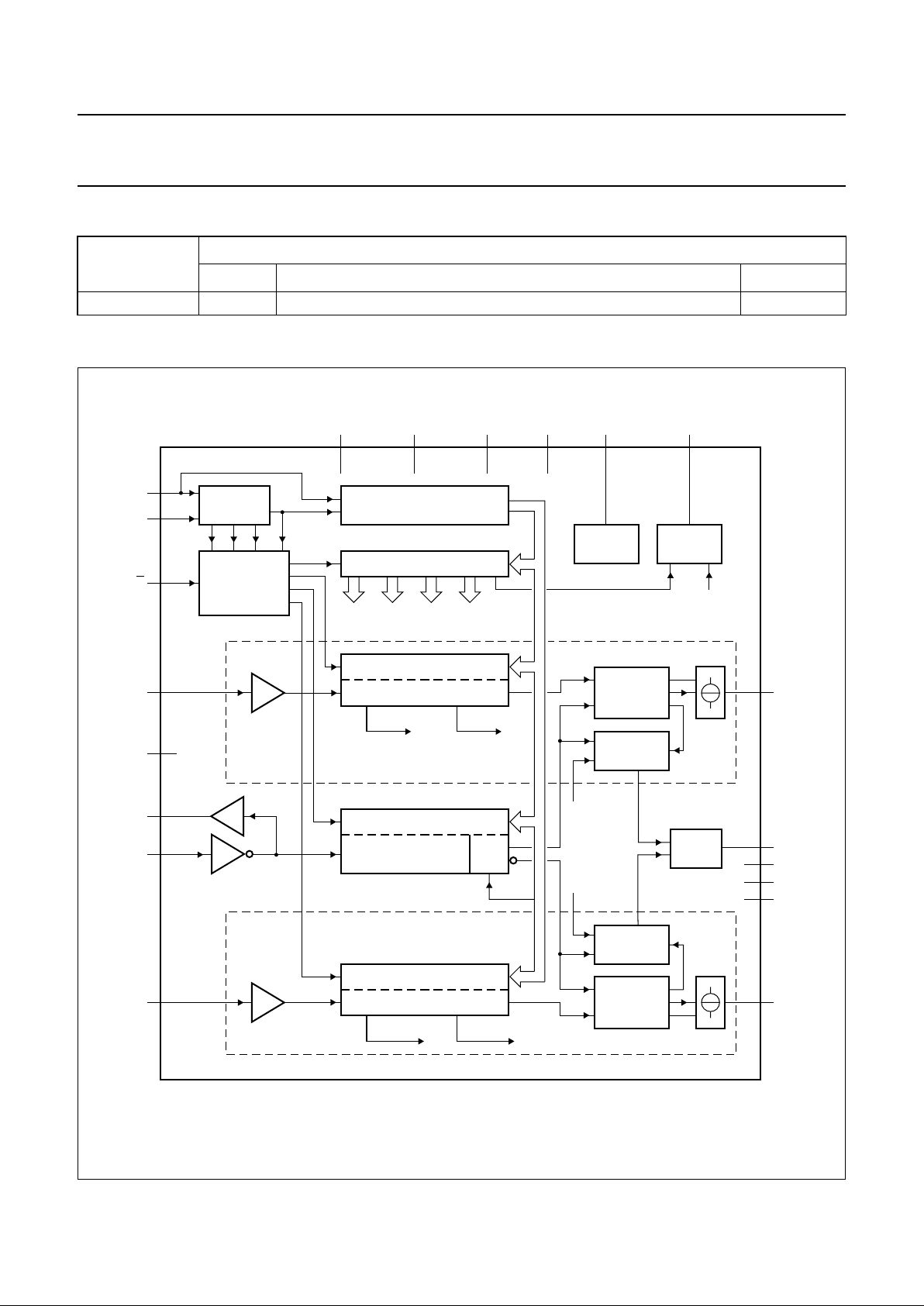
BLOCK DIAGRAM
TYPE NUMBER
PACKAGE
NAME DESCRIPTION VERSION
UMA1015AM SSOP20 plastic shrink small outline package; 20 leads; body width 4.4 mm SOT266-1
Fig.1 Block diagram.
handbook, full pagewidth
MGG523
4-BIT SHIFT
REGISTER
CONTROL LATCH
power
down
OOL
select
current
ratio
port
bits
17-BIT SHIFT REGISTER
LATCH
MAIN DIVIDER
TOOL A
RFA/64
LATCH
MAIN DIVIDER
TOOL B RFB/64
LATCH
REFERENCE DIVIDER
DIV
BY 2
ADDRESS
DECODER
PHASE
DETECTOR
LOCK
DETECTOR
PHASE
DETECTOR
LOCK
DETECTOR
LOCK
SELECT
TOOL A
TOOL B
PUMP
BIAS
VOLTAGE
DOUBLER
SR
SYNTHESIZER A
SYNTHESIZER B
11
12
13
6
5
10
8
15
4
14
7
16
20
18
3
19
1
2
9
17
CLK
DATA
E
RFA
HPD
f
XTALO
f
XTALIN
RFB
V
DD1
V
DD2
DGND AGND
I
SET
V
CC
CPA
P0/OOL
P1
P2
P3
CPB
VDB enable
RF/64
phase
error
phase
error
UMA1015AM
1997 Sep 03 4
Philips Semiconductors Product specification
Low-power dual frequency synthesizer
for radio communications
UMA1015AM
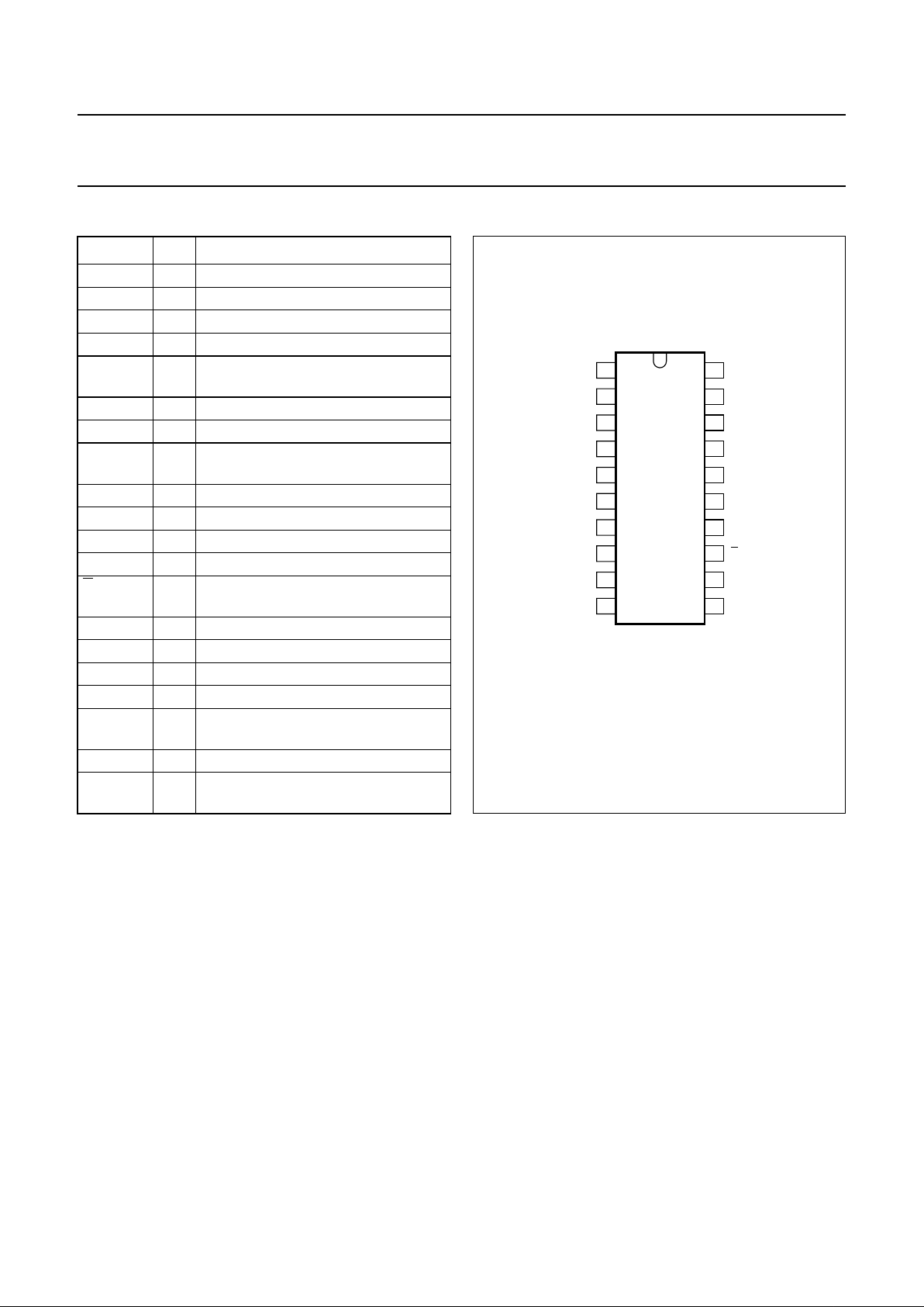
PINNING
SYMBOL PIN DESCRIPTION
P1 1 output Port 1
P2 2 output Port 2
CPA 3 charge pump output synthesizer A
V
DD1
4 digital supply voltage 1
HPD 5 hardware power-down
(input LOW = power-down)
RFA 6 RF input synthesizer A
DGND 7 digital ground
f
XTALIN
8 common crystal frequency input from
TCXO
P3 9 output Port 3
f
XTALO
10 open-drain output of f
XTAL
signal
CLK 11 programming bus clock input
DATA 12 programming bus data input
E 13 programming bus enable input
(active LOW)
V
DD2
14 digital supply voltage 2
RFB 15 RF input synthesizer B
AGND 16 analog ground to charge pumps
CPB 17 charge pump output synthesizer B
V
CC
18 analog supply to charge pump;
external or voltage doubler output
P0/OOL 19 Port output 0/out-of-lock output
I
SET
20 regulator pin to set charge pump
currents
Fig.2 Pin configuration.
handbook, halfpage
P1
P2
CPA
V
DD1
HPD
RFA
DGND
f
XTALIN
P3
f
XTALO
I
SET
P0/OOL
V
CC
CPB
RFB
V
DD2
AGND
E
DATA
CLK
1
2
3
4
5
6
7
8
9
10
11
12
20
19
18
17
16
15
14
13
UMA1015AM
MGG522
FUNCTIONAL DESCRIPTION
Main dividers
Each synthesizer has a fully programmable 17-bit main
divider. The RF input drives a pre-amplifier to provide the
clock to the first divider bit. The pre-amplifier has a high
input impedance, dominated by pin and pad capacitance.
The circuit operates with signal levels from below
50 mV (RMS) up to 250 mV (RMS), and at frequencies up
to 1.1 GHz. The high frequency sections of the divider are
implemented using bipolar transistors, while the slower
section uses CMOS technology. The range of division
ratios is 512 to 131071.
Reference divider
There is a common fully programmable 12-bit reference
divider for the two synthesizers. The input f
XTALIN
drives a
pre-amplifier to provide the clock input for the reference
divider. This clock signal is also inverted and output on pin
f
XTALO
(open drain). A crystal connected between f
XTALIN
and f
XTALO
with suitable feedback components can be
used to make an oscillator. An extra divide-by-2 block
allows a reference comparison frequency for
synthesizer B to be half the frequency of synthesizer A.
This feature is selectable using the program bit SR. If the
programmed reference divider ratio is R then the ratio for
each synthesizer is as given in Table 1.
The range for the division ratio R is 8 to 4095. Opposite
edges of the divider output are used to drive the phase
detectors to ensure that active edges arrive at the phase
detectors of each synthesizer at different times. This
minimizes the potential for interference between the
charge pumps of each loop. The reference divider consists
of CMOS devices operating beyond 35 MHz.

1997 Sep 03 5
Philips Semiconductors Product specification
Low-power dual frequency synthesizer
for radio communications
UMA1015AM
Table 1 Synthesizer ratio of reference divider
Phase comparators
For each synthesizer, the outputs of the main and
reference dividers drive a phase comparator where a
charge pump produces phase error current pulses for
integration in an external loop filter. The charge pump
current is set by an external resistance R
SET
at pin I
SET
,
where a temperature-independent voltage of 1.1 V is
generated. R
SET
should be between 12 and 60 kΩ.
The charge pump current, ICP, can be programmed to be
either (12 × I
SET
) or (24 × I
SET
) with a maximum of 2.3 mA.
The dead zone, caused by finite switching of current
pulses, is cancelled by an internal delay in the phase
detector thus giving improved linearity. The charge pump
has a separate supply, VCC, which helps to reduce the
interference on the charge pump output from other parts of
the circuit. VCC can be higher than V
DD1
if a wider range on
the VCO input is required. VCC must not be less than V
DD1
.
Voltage doubler
If required, there is a voltage doubler on-chip to supply the
charge pumps at a higher level than the nominal available
supply. The doubler operates from the digital supply V
DD1
,
and is internally limited to a maximum output of 6 V.
An external capacitor is required on pin VCC for smoothing,
the capacitor required to develop the extra voltage is
integrated on-chip. To minimize the noise being introduced
to the charge pump output from the voltage doubler, the
doubler clock is suppressed (provided both loops are
in-lock) for the short time that the charge pumps are active.
The doubler clock (RF/64) is derived from whichever main
divider is operating (synthesizer A has priority). While both
synthesizers are powered down (and the doubler is
enabled), the doubler clock is supplied by a low-current
internal oscillator. The doubler can be disabled by
programming the bit VDON to logic 0, in order to allow an
external charge pump supply to be used.
Out-of-lock indication/output ports
There is a common lock detector on-chip for the
synthesizers. The lock condition of each, or both loops, is
output via an open-drain transistor which drives
pin P0/OOL (when out-of-lock, the transistor is turned on
and therefore the output is forced LOW). The lock
condition output is software selectable (see Table 4).
SR SYNTHESIZER A SYNTHESIZER B
0R R
1R 2R
An out-of-lock condition is flagged when the phase error is
greater than T
OOL
, which is approximately 30 ns.
The out-of-lock flag is only released after the first reference
cycle where the phase error is less than T
OOL
.
The out-of-lock function can be disabled, via the serial bus,
and the pin P0/OOL can be used as a port output. Three
other port outputs P1, P2 and P3 (open-drain transistors)
are also available.
Serial programming bus
A simple 3-line unidirectional serial bus is used to program
the circuit. The 3 lines are DATA, CLK and
E (enable).
The data sent to the device is loaded in bursts framed
by E. Programming clock edges are ignored until E goes
active LOW. The programmed information is loaded into
the addressed latch when E returns inactive (HIGH). This
is allowed when CLK is in either state without causing any
consequences to the register data. Only the last 21 bits
serially clocked into the device are retained within the
programming register. Additional leading bits are ignored,
and no check is made on the number of clock pulses.
The fully static CMOS design uses virtually no current
when the bus is inactive. It can always capture new
programming data even during power-down of both
synthesizers.
However when either synthesizer A or synthesizer B or
both are powered-on, the presence of a TCXO signal is
required at pin 8 (f
XTALIN
) for correct programming.
Data format
Data is entered with the most significant bit first.
The leading bits make up the data field, while the trailing
four bits are an address field. The address bits are
decoded on the rising edge of
E. This produces an internal
load pulse to store the data in the addressed latch.
To ensure that data is correctly loaded on first power-up,
E should be held LOW and only taken HIGH after having
programmed an appropriate register. To avoid erroneous
divider ratios, the pulse is inhibited during the period when
data is read by the frequency dividers. This condition is
guaranteed by respecting a minimum E pulse width after
data transfer. The data format and register bit allocations
are shown in Table 2.
1997 Sep 03 6
Philips Semiconductors Product specification
Low-power dual frequency synthesizer
for radio communications
UMA1015AM
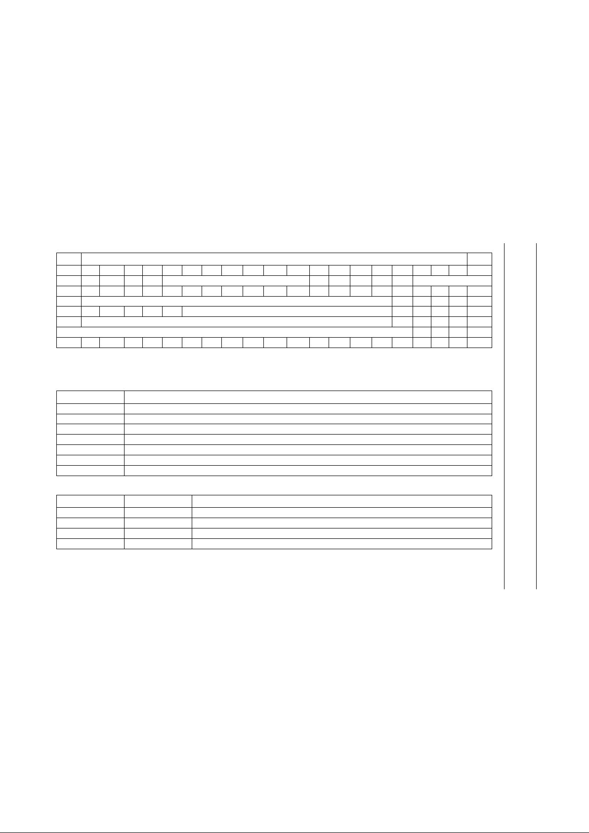
Table 2 Bit allocation
Note
1. The test register should not be programmed with any other values except all zeros for normal operation.
Table 3 Bit allocation description
Table 4 Out-of-lock select
FIRST REGISTER BIT ALLOCATION LAST
p1 p2 p3 p4 p5 p6 p7 p8 p9 p10 p11 p12 p13 p14 p15 p16 p17 p18 p19 p20 p21
dt16 dt15 dt14 dt13 dt12 DATA FIELD dt4 dt3 dt2 dt1 dt0 ADDRESS
X X VDON PO OLA OLB CRA CRB X X sPDA sPDB P3 P2 P1 X X 0 0 0 1
MA16 SYNTHESIZER A MAIN DIVIDER COEFFICIENT MA0 0 1 0 0
0 0 0 0 SR R11 REFERENCE DIVIDER COEFFICIENT R0 0 1 0 1
MB16 SYNTHESIZER B MAIN DIVIDER COEFFICIENT MB0 0 1 1 0
RESERVED FOR TEST
(1)
000 0
0 00 000000 00 0 00sPBF 0 0 1 0 0 0
SYMBOL DESCRIPTION
sPDA, sPDB software power-down for synthesizers A and B (0 = power-down)
sPBF software power-on for f
xtal
buffer (1 = buffer on)
P3, P2, P1 and P0 bits output to pins 1, 2, 9 and 19 (1 = high impedance)
VDON voltage doubler enable (1 = doubler enabled)
OLA, OLB out-of-lock select; selects signal output to pin 19 (see Table4)
CRA, CRB charge pump A/B current to I
SET
ratio select (see Table 5)
SR reference frequency ratio select (see Table 6)
OLA OLB OUTPUT AT PIN 19
00P0
0 1 lock status of loop B; OOLB
1 0 lock status of loop A; OOLA
1 1 logic OR function of loops A and B
1997 Sep 03 7
Philips Semiconductors Product specification
Low-power dual frequency synthesizer
for radio communications
UMA1015AM
Table 5 Charge pump current ratio
Table 6 Reference division ratio
Power-down modes
The device can be powered down either via pin HPD
(active LOW = power-down) or via the serial bus
(bits sPDA and sPDB, logic 0 = power-down).
CRA/CRB CURRENT AT PUMP
0I
CP
=12×I
SET
1I
CP
=24×I
SET
SR SYNTHESIZER A SYNTHESIZER B
0R R
1R 2R
The synthesizers are powered up when both hardware
and software Power-down signals are at logic 1. When
only one synthesizer is powered down, the functions
common to both will be maintained (independent of the
state of sPBF). When both synthesizers are powered
down, the f
xtal
buffer can be maintained in an active state
by setting sPBF to logic 1. This will allow any system clock
derived from the f
XTALO
buffered output to remain on in
power-down. Note that sPBF is independent of the state of
HPD. When both synthesizers are switched off, the
voltage doubler (if enabled) will remain active drawing a
reduced current. An internal oscillator will drive the doubler
in this situation. If both synthesizers have been in a
power-down condition, then when one or both
synthesizers are reactivated, the reference and main
dividers restart in such a way as to avoid large random
phase errors at the phase comparator.
LIMITING VALUES
In accordance with the Absolute Maximum Rating System (IEC 134).
HANDLING
Inputs and outputs are protected against electrostatic discharge in normal handling. However, to be totally safe, it is
desirable to take normal precautions appropriate to handling MOS devices.
SYMBOL PARAMETER MIN. MAX. UNIT
V
DD1
, V
DD2
DC range of digital power supply voltage with respect to DGND −0.3 +6.0 V
V
CC
DC charge pump supply voltage with respect to AGND −0.3 +6.0 V
∆V
CC-DD
difference in voltage between VCC and V
DD1
, V
DD2
−0.3 +6.0 V
V
n
DC voltage at pins 1, 2, 5, 6, 8 to 15, 19 and 20 with respect to DGND −0.3 V
DD1
+ 0.3 V
V
3, 17
DC voltage at pins 3 and 17 with respect to AGND −0.3 VCC+ 0.3 V
∆V
GND
difference in voltage between AGND and DGND (these pins should be
connected together)
−0.3 +0.3 V
T
stg
storage temperature −55 +125 °C
T
amb
operating ambient temperature −30 +85 °C
1997 Sep 03 8
Philips Semiconductors Product specification
Low-power dual frequency synthesizer
for radio communications
UMA1015AM
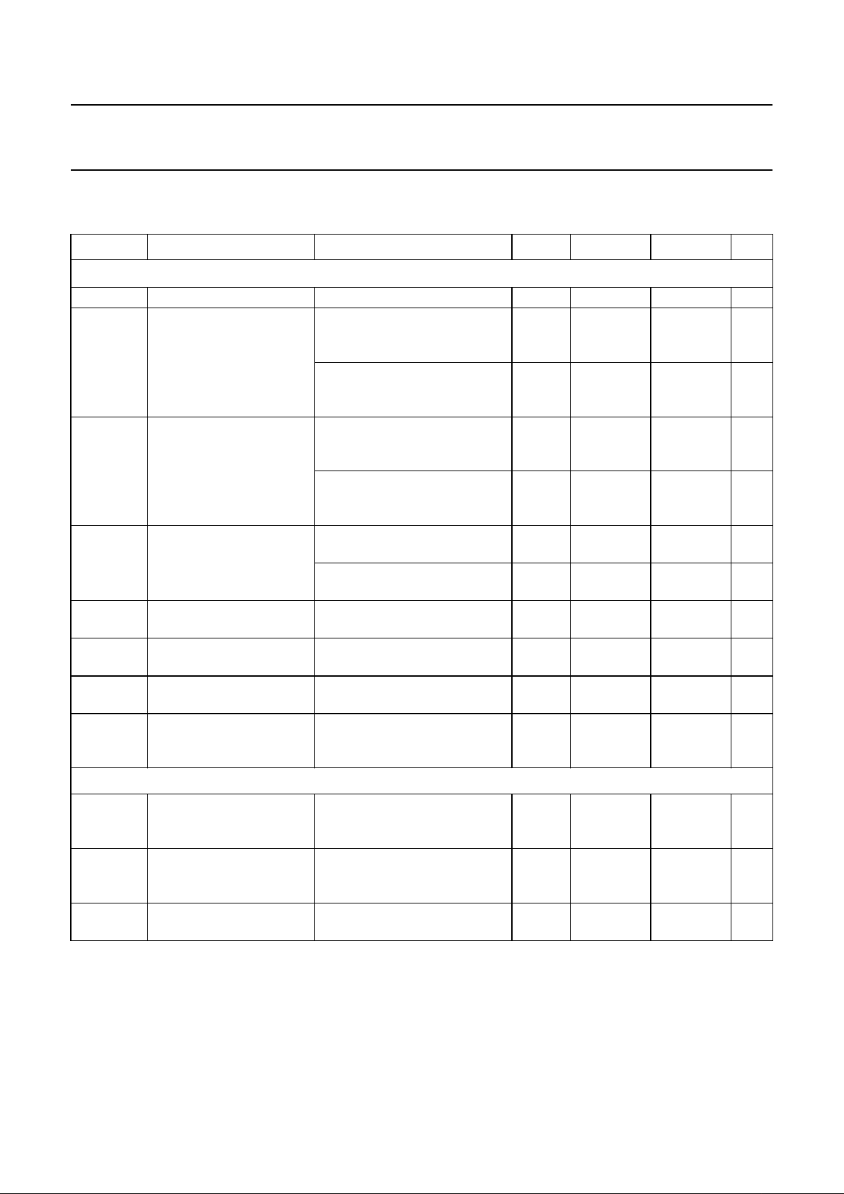
CHARACTERISTICS
V
DD1=VDD2
= 2.7 to 5.5 V; VCC= 2.7 to 6.0 V; T
amb
=25°C; unless otherwise specified.
SYMBOL PARAMETER CONDITIONS MIN. TYP. MAX. UNIT
Supplies; (V
DD1
, V
DD2
and VCC) voltage doubler disabled, external supply on V
CC
V
DD1
, V
DD2
digital supply voltage V
DD1=VDD2
2.7 − 5.5 V
I
DD1+IDD2
total digital supply current
from V
DD1
and V
DD2
f
XTAL
= 12.8 MHz;
both synthesizers on;
V
DD1=VDD2
=3V
− 8.7 − mA
f
XTAL
= 12.8 MHz;
both synthesizers on;
V
DD1=VDD2
= 5.5 V
−− 12.5 mA
I
DDpda
,
I
DDpdb
total digital supply current
from V
DD1
and V
DD2
with
one synthesizer in
power-down mode
f
XTAL
= 12.8 MHz; one
synthesizer powered down;
V
DD1=VDD2
=3V
− 5.0 − mA
f
XTAL
= 12.8 MHz; one
synthesizer powered down;
V
DD1=VDD2
= 5.5 V
−− 7.5 mA
I
DD(xtal)
digital supply current from
V
DD1
with both
synthesizers powered
down and crystal buffer on
f
XTAL
= 12.8 MHz; V
HPD
=0V;
sPBF = 1; V
DD1=VDD2
=3V
− 0.5 − mA
f
XTAL
= 12.8 MHz; V
HPD
=0V;
sPBF = 1; V
DD1=VDD2
= 5.5 V
−− 1.15 mA
I
DDpd
digital supply current in
power-down mode
both synthesizers powered
down; V
HPD
= 0 V; sPBF = 0
−− 60 µA
V
CC
charge pump supply
voltage
VCC≥ V
DD
2.7 − 6.0 V
I
CC
charge pump supply
current
both synthesizers on and in
lock; f
ref
= 12.5 kHz
−− 25 µA
I
CCpd
charge pump supply
current in power-down
mode
both synthesizers powered
down
−− 25 µA
Voltage doubler enabled
I
DD
total digital supply current
from V
DD1
and V
DD2
f
XTAL
= 12.8 MHz; both
synthesizers on and in lock;
V
DD1
=3V; fRF= 900 MHz
− 9.2 12 mA
I
DDpd
total digital supply current
in power-down mode from
V
DD1
and V
DD2
both synthesizers powered
down; V
DD1
=3V; V
HPD
=0V;
sPBF = 0
− 0.25 0.4 mA
V
CCvd
charge pump supply
voltage
DC current drawn from
VCC=50µA; fRF> 100 MHz
4.2 2V
DD1
− 0.6 6.0 V
 Loading...