

Philips UMA1002T Datasheet

INTEGRATED CIRCUITS
DATA SH EET
UMA1002
Data processor for cellular radio
(DPROC2)
Product specification
Supersedes data of 1996 Sep 13
File under Integrated Circuits, IC17
1997 Jan 28
Philips Semiconductors Product specification
Data processor for cellular radio
(DPROC2)
FEATURES
• Single chip solution to all the data handling and
supervisory functions
• Configuration to both AMPS and TACS
• Additional JTACS option
• I2C-bus serial control
• All analog interface and filtering functions fully
implemented on chip
• Error handling in hardware reduces software
requirements
• Robust SAT decoding and transponding circuitry
• Low current consumption by on-chip power-down
modes
• Reduced system current consumption by new
integrated power-saving features
– Majority voting includes more intelligence
– On-chip control filler word filter
– BCH error filter
– Possibility to program ESCC bits
• Small physical size: SO28 or LQFP32
• External peripheral component count reduced
– On-chip selectable clock divider
– Integrated pull-up resistor at TXLINE
• Simplified reset and abort software routines possible
• The SO28 version is fully compatible with UMA1000LT
and UMF1000T.
UMA1002
GENERAL DESCRIPTION
The UMA1002 is a low power CMOS LSI device
incorporating the data transceiving, data processing, and
SAT functions (including on-chip filtering) for an AMPS or
TACS hand-held portable cellular radio telephone.
In this data sheet, the UMA1002 is often referred to by the
descriptive term ‘DPROC2’.
QUICK REFERENCE DATA
SYMBOL PARAMETER MIN. TYP. MAX. UNIT
V
DD
I
DD
T
amb
ORDERING INFORMATION
TYPE
NUMBER
UMA1002T SO28 plastic small outline package; 28 leads; body width 7.5 mm SOT136-1
UMA1002H LQFP32 plastic low profile quad flat package; 32 leads; body 7 × 7 × 1.4 mm SOT358-1
1997 Jan 28 2
supply voltage 2.7 3.0 5.5 V
supply current normal operation with external clock − 1.3 1.8 mA
operating ambient temperature −30 − +70 °C
PACKAGE
NAME DESCRIPTION VERSION

1997 Jan 28 3
b
ook, full pagewidth
BLOCK DIAGRAM
(DPROC2)
V
DDAVDDD INVRX RECDATA MVO
Philips Semiconductors Product specification
Data processor for cellular radio
DEMODD
AGND
DATA
RESET
3
ANTI-
ALIASING
(31)
FILTER
UMA1002
2 (30)
4
(32)
6
RESET, CLOCK AND
POWER-DOWN
(2)
GENERATOR
(3)10 (8)7 (4)28 (27)(28)
COMPARATOR 1
DATA
RECOVERY
SAT
FILTER
CLOCK
FILTER
12 (10)(20)
13 (11)
CLKOUTCLKINCLKSEL
INTERPOLATOR
BIAS
GENERATOR
OUTPUT
FILTER
TEST
LOGIC
9
(7)22(22)
TST TSCAN
COMPARATOR 2
GATED D/A
GATED D/A
1 (29)
SSA
SAT
RECOVERY
SAT
REGENERATION
ST
GENERATOR
14 (12)
V
SSD
SYNCRONIZATION
AND VOTING
DOTTING
DETECTOR
SAT
DETERMINATION
MANCHESTER
AND BCH
ENCODING
(6) 21 (21)
ERROR
CORECTION
ARBITRATION
LOGIC
TRANSMIT
BUFFER
2
I C
INTERFACE
23
(23)
A0INVTXJTACSV
8 (5)
27 (26)
19 (17)
5 (1)
20 (19)
11 (9)
18 (16)
17 (15)
15 (13)
25 (25)
24 (24)
RXLINE
RXCLK
BUSY/VSAT
RACTRL
TXCTRL
TACTRL
TXCLK
TXHOLD
TXLINE
SCL
SDA
MBD827
Pins in parenthesis apply to UMA1002H in LQFP32.
UMA1002
Fig.1 Block diagram.
Philips Semiconductors Product specification
Data processor for cellular radio
UMA1002
(DPROC2)
PINNING
SYMBOL
V
SSA
AGND 2 30 Internally generated analog signal ground. V oltage level =
DEMODD 3 31 DEMODD inputs analog data and SAT signals from the RF demodulator. This pin
DA TA 4 32 Data is an analog output which provides the Manchester encoded and filtered data
RACTRL 5 1 Received audio control output. Open-drain output used to blank the audio path to
RESET 6 2 Master reset input resetting all internal flip-flops to the specified state. This input
INVRX 7 4 This input inverts the sense of received data stream, which allows RF
RXLINE 8 5 Received data signal output to the system controller.
TST 9 7 Test input pin (note 1).
RECDATA 10 8 Output of the recovered digital data signal (note 1).
TACTRL 11 9 Transmitter audio control output. This open-drain output is used to blank the audio
CLKIN 12 10 1.2 MHz or 9.6 MHz external master clock input. This input signal should be
CLKOUT 13 11 Output of 1.2 MHz clock signal (for APROC) derived from CLKIN.
V
SSD
TXLINE 15 13 Open-drain bidirectional data line to the system controller (internal 100 kΩ pull-up).
n.c. 16 14 Not connected.
TXHOLD 17 15 This input holds off transmission of data when set to HIGH.
TXCLK 18 16 Transmitted data clock input from the system controller.
BUSY/VSA T 19 17 Output indicating the status of the RECC by providing output information based on
PIN
DESCRIPTION
SO28 LQFP32
1 29 Negative analog supply (0 V). To be connected low-ohmic to V
1
.
SSD
⁄2V
. This pin should
DDA
be connected to a blocking capacitor, no DC load allowed.
should normally be AC-coupled. See Chapter “AC characteristics”.
signal, SAT and signalling tone. This signal should normally be AC-coupled into the
Audio/Data summer. See Chapter “AC characteristics”.
the earpiece when a sequence of dotting followed by a synchronization word or 2
synchronization words separated by 77 bits is detected. RACTRL and TACTRL
functions can be combined using one line. Output level LOW means audio muted.
has no influence on analog parts, but must be controlled by an active HIGH
microcontroller port.
demodulators with high or low local oscillators to be used. The AMPS and TACS
specifications define NRZ encoded logic 1 as a LOW-to-HIGH transition in the
centre of a data bit period. The polarity of the demodulated data stream into
DPROC2 depends on the receiver local oscillator. Input LOW means data normal.
path and enable the data path to the modulator during data bursts on the RVC.
Output level LOW means audio muted.
accurate to 100 × 10
−6
and have a worst case 60 : 40 mark-space ratio.
14 12 Negative digital supply (0 V), internally connected to substrate. To be connected
low-ohmic to V
SSA
.
a majority decision on the last 3 consecutive Busy/Idle bits (FVC = logic 0). Output
level LOW means channel idle.
Indicating the result of the comparison of the measured SA T and the expected SAT
colour-code bits (I
2
C-bus register) in the voice channel mode (FVC = logic 1 and
ENSM = logic 1). Output level LOW means incoming SAT not equal to expected
SAT.
1997 Jan 28 4
Philips Semiconductors Product specification
Data processor for cellular radio
UMA1002
(DPROC2)
SYMBOL
TXCTRL 20 19 Transmitter control open-drain output used to disable the transmitter during an
INVTX 21 21 This input inverts the sense of transmitted data stream, which allows RF
TSCAN 22 22 Test switch input, only enabled if TST = logic 1, but should have a defined state.
A0 23 23 Input to select the least significant bit of the I
SDA 24 24 Serial data input/output (I
SCL 25 25 Serial clock input (I
n.c. 26 18 Not connected.
RXCLK 27 26 Received data clock input from the system controller.
V
DDD
V
DDA
MVO − 3 Majority voting output indicating that on FOCC the first 3 received words do not
JTACS − 6 Digital input signal for JTACS, input HIGH means that data is routed from TXLINE
CLKSEL − 20 Input switch for internal divide-by-8 or divide-by-1 divider between CLKIN and
PIN
SO28 LQFP32
RECC access failure. Output level LOW means RF disabled.
modulators with high or low local oscillators to be used. The AMPS and TACS
specifications define NRZ encoded logic 1 as a LOW-to-HIGH transition in the
centre of a data bit period. The polarity of the modulated data stream depends on
the transmitter local oscillator. Input LOW means data inverted.
2
C-bus).
28 27 Digital supply voltage (+3 V).
− 28 Analog supply voltage (+3 V).
differ from each other and thus the majority decision over 5 words can already be
carried out. Because of the required speed, indication is at this pin (and not via the
2
I
C-bus) which can be monitored by the system controller. Output LOW means the
receiver can be switched off.
directly without processing to gated D/A converter (if enabled by STEN bit).
CLKOUT (internal pull-down → divide-by-1 is default if not bonded out in SO28
package).
2
C-bus).
DESCRIPTION
2
C-bus address.
Note
1. Must not be connected in existing applications.
1997 Jan 28 5
Philips Semiconductors Product specification
Data processor for cellular radio
(DPROC2)
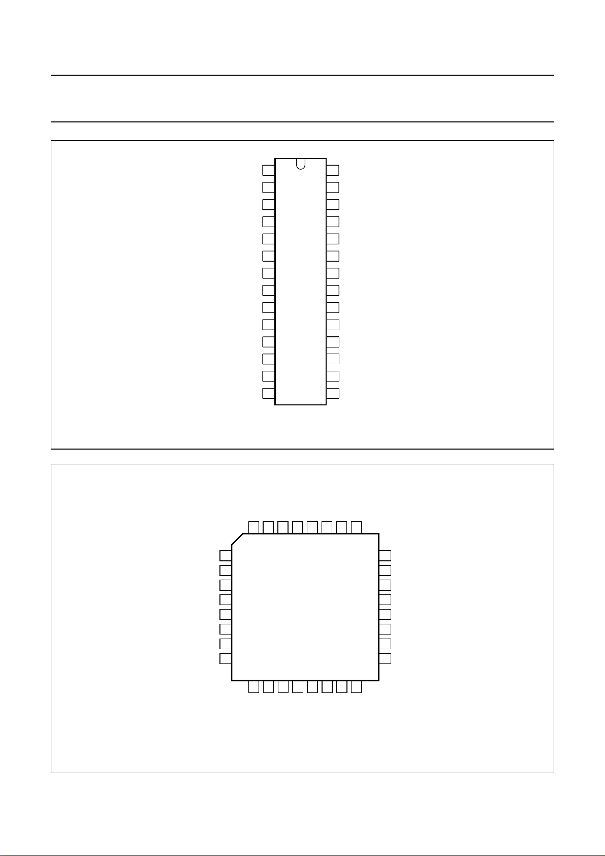
handbook, halfpage
V
SSA
AGND
DEMODD
DATA
RACTRL
RESET
INVRX
RXLINE
TST
RECDATA
TACTRL
CLKIN
CLKOUT
V
SSD
1
2
3
4
5
6
7
8
9
10
11
12
13
UMA1002T
MBD828
V
28
DDD
27
RXCLK
n.c.
26
25
SCL
24
SDA
23
A0
22
TSCAN
21
INVTX
20
TXCTRL
19
BUSY/VSAT
18
TXCLK
17
TXHOLD
16
n.c.
1514
TXLINE
UMA1002
handbook, full pagewidth
Fig.2 Pin configuration for SO28, SOT136-1.
SSA
DDA
SSD
DDD
V
28
27
13
14
n.c.
TXLINE
RACTRL
RESET
MVO
INVRX
RXLINE
JTACS
TST
RECDATA
DATA
AGNDVV
DEMODD
32
31
30
29
1
2
3
4
5
6
7
8
9
10
CLKIN
TACTRL
UMA1002H
11
12
V
CLKOUT
RXCLK
SCL
26
25
15
16
TXCLK
TXHOLD
24
SDA
23
A0
22
TSCAN
INVTX
21
20
CLKSEL
19
TXCTRL
18
n.c.
BUSY/VSAT
17
MBD829
Fig.3 Pin configuration for LQFP32, SOT358-1.
1997 Jan 28 6

Philips Semiconductors Product specification
Data processor for cellular radio
(DPROC2)
FUNCTIONAL DESCRIPTION
General
The UMA1002 (DPROC2) is a single-chip CMOS device
which handles the data and supervisory functions of an
AMPS or TACS subscriber set.
These functions are:
• Data reception and transmission
• Control and voice channel exchanges
• Error detection, correction, decoding and encoding
• Supervisory Audio Tone decoding and transponding
• Signalling Tone generation.
In an AMPS or TACS cellular telephone system, mobile
stations communicate with a base over full duplex RF
channels. A call is initially set up using one out of a number
of dedicated control channels. This establishes a duplex
voice connection using a pair of voice channels.
Any further transmission of control data occurs on these
voice channels by briefly blanking the audio and
simultaneously transmitting the data. The data burst is
brief and barely noticeable by the user. A data rate of
10 kbits/s is used in the AMPS system and 8 kbits/s in
TACS. The signalling formats for both Forward Channels
(base to mobile) and Reverse Channels (mobile to base)
are shown in Fig.14.
A function known as Supervisory Audio Tone (SAT), a set
of 3 audio tones (5970, 6000 and 6030 Hz), is used to
indicate the presence of the mobile on the designated
voice channel. This signal, which is analogous to the
On-Hook signal on land lines, is sent out to the mobile by
the base station on the Forward Voice Channel. The signal
must be accurately recovered and transponded back to
the base station to complete the ‘loop’. At the base station
this signal is used to ascertain the overall quality of the
communication link.
Another voice channel associated signal is Signalling
Tone (ST). This tone (8 kHz TACS, 10 kHz AMPS) is
generated by the mobile and is sent in conjunction with
SAT on the Reverse Voice Channel to serve as an
acknowledgement signal to a number of system orders.
The key requirements of a hand-held portable cellular set
are:
• Small physical size
• Minimum number of interconnections (serial bus)
• Low power consumption
• Low cost.
UMA1002
The DPROC2 is a member of our Cellular Radio chip set,
based on the I
A cellular radio system schematic using the chip set is
shown in Fig.11.
DPROC2 power-saving features
To support current saving in the application, DPROC2 has
three different modes of circuit operation implemented.
They are decoded by the I
activity on the data transfer link (TXCLK and TXLINE).
In power-down mode the relevant digital circuits have the
clock disabled, the analog circuits have the bias currents
and the switched capacitor clock switched off.
• Normal mode: all circuit parts are operating (e.g. on
Voice channels)
• Power-down mode 1: the SAT path is in power-down
(e.g. during access of the RECC)
• Power-down mode 2: the SAT path and the total data
transmit path are in power-down (e.g. for Idle state,
DPROC2 operating only on FOCC).
System power-saving features
Besides the above mentioned power-down modes
DPROC2 also includes features to reduce system current
(e.g. switching off parts of the receiver, and put the system
controller into Idle mode for longer periods of time).
All these features are controlled by the I
explanation of the following features refer to the Section
“I2C-bus serial data link (SDA; SCL)” sub-section “I2C-bus
registers”.
M
AJORITY VOTING (ONLY IN LQFP32)
Majority voting includes more intelligence. This feature is
enabled in FOCC with I2C-bus bit MAJ = logic 1.
If 3 consecutive identical words have been received it is
signalled via pin MVO. Therefore during the last 2 frame
words the receiver could be switched off to save system
current consumption.
C
ONTROL FILLER WORDS FILTER
System current can be further reduced by an on-chip
control filler words filter in FOCC, which enables the
detection of consecutive identical control filler words.
If consecutive control filler words are identical (i.e. DCC,
CMAC and WFOM) they will not be passed on to the
microcontroller. Consequently the system controller can
remain in power-saving mode.
2
C-bus, which meets these requirements.
2
C-bus register bit FVC and by
2
C-bus. For further
1997 Jan 28 7
Philips Semiconductors Product specification
Data processor for cellular radio
(DPROC2)
PROGRAMMING OF ESCC BITS
There is a possibility to program the expected ESCC bits,
so that DPROC2 can compare expected and received
SAT and signal any inconsistency to the system controller
via BUSY/VSAT pin. Consequently there is no need to
read the measured SAT periodically via the I2C-bus.
BCH
ERROR FILTER
If this feature is enabled, DPROC2 will not pass on to the
microcontroller words with BCH errors. Consequently the
microcontroller can remain in power-saving mode. This
feature in combination with the control filler feature is
defined in Table 8.
S
ELECTABLE CLOCK DIVIDER (ONLY IN LQFP32)
An on-chip selectable divide-by-8 clock divider reduces
external peripheral component count.
UMA1002
Power-up state and master reset (RESET)
RESET should be HIGH as soon as power supply is
available.
DPROC2 will not respond reliably to any inputs (including
RESET) until 100 µs after the power supply has settled
within the specified tolerance. The analog sections of the
device will have stabilized within 5 ms. No on-chip
power-on reset is provided, therefore before the device
can enter normal operation RESET must be held HIGH.
RESET is an active HIGH master reset input, with a
minimum active pulse width of 4 µs which may be used to
reset the total logic within DPROC2 to a predefined state
as illustrated in Tables 1 and 2. It is preferably only used
during power-up, during normal operation it is
recommended to use the fully synchronous reset signals
derived from the I2C-bus bits FVC, STS and TXRST
(see Table 4). To ensure correct operation TXCLK must
be held HIGH during RESET operation.
Table 1 Predefined state of the digital output pins
OUTPUT STATE
RXLINE HIGH
TXCTRL high-impedance (HIGH)
TACTRL high-impedance (HIGH)
RACTRL high-impedance (HIGH)
BUSY/VSAT HIGH
TXLINE HIGH (by 100 kΩ internal pull-up resistor)
RECDATA LOW
MVO HIGH
SDA high-impedance (HIGH)
2
Table 2 Predefined state of the I
REGISTER
76543210
Status (read) LOW LOW LOW HIGH LOW LOW HIGH HIGH
Control 1 (write) LOW LOW LOW LOW LOW LOW LOW LOW
Control 2 (write) LOW LOW LOW LOW LOW LOW LOW LOW
C-bus registers
BIT
1997 Jan 28 8
Philips Semiconductors Product specification
Data processor for cellular radio
(DPROC2)
I2C-bus serial data link (SDA; SCL)
SDA is the bidirectional data line, SCL is the clock input
from an I2C-bus master. These constitute a typical I2C link
and conform to standard I2C-bus characteristics.
A detailed description of the I2C-bus specification, with
applications, is given in the brochure
how to use it”.
This brochure may be ordered using the
code 9398 393 40011.
• Data rate up to 100 kbits/s.
S
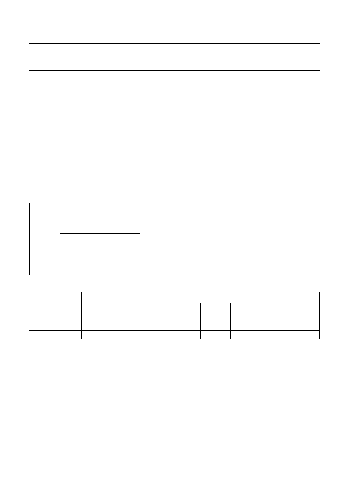
LAVE ADDRESS SELECT (A0)
Selection of the device slave address is achieved by
connecting A0 to either VSS or V
defined in accordance with the I2C-bus specifications as
shown in Fig.4.
handbook, halfpage
“The I2C-bus and
. The slave address is
DDD
(1)
R/W11011XA0
MBD831
UMA1002
I2C-BUS REGISTERS
The I2C-bus register block resides internally within the
I2C-bus interface block and contains various items of
status and control information which are transferred to and
from DPROC2 via the I2C-bus. The block is organized into
three 8-bit registers:
• Status register which contains read only items
• Control registers 1 and 2 which contain write only items.
(1) X = don’t care.
Fig.4 Device slave address.
Table 3 I2C-bus register map
BIT
REGISTER
76543210
Status (read) −−WSYNC BUSY TXABRT TXIP MSCC1 MSCC0
Control 1 (write) BUFEN SERV STS TXRST ABREN FVC STEN SATEN
Control 2 (write) MAJ MR1 MR0 DBCH DCFM ENSM ESCC1 ESCC0
1997 Jan 28 9

Philips Semiconductors Product specification
Data processor for cellular radio
(DPROC2)
handbook, full pagewidth
(a) Read from DPROC2 status register.
(b) Write to DPROC2 control register 1.
(c) Write to all DPROC2 control registers.
Where:
S = START condition
W = read/write bit (logic 0 = write)
R = read/write bit (logic 1 = read)
A = acknowledge bit
P = STOP condition
DPROC ADR = slave address of DPROC2.
DPROC ADRS R A STATUS
P
(a)
WA APDPROC ADRS
CONTROL 1
(b)
WA ADPROC ADRS CONTROL 2 A P
CONTROL 1
MBD832
(c)
UMA1002
Fig.5 I2C-bus data format.
1997 Jan 28 10

Philips Semiconductors Product specification
Data processor for cellular radio
UMA1002
(DPROC2)
Table 4 Description of I2C-bus register map
REGISTER
BITS
Control Register 1
BUFEN 0 1.2 MHz signal not available at pin CLKOUT
SERV 0 serving system data stream B selected
(1)
STS
TXRST 1 terminates a message being transmitted on the reverse channel; monostable
ABREN 1 DPROC2 has permission to abort data transmission and disable RF on the RECC
(2)
FVC
STEN 0 disables output of signalling tone to pin DATA
SATEN 0 disables output of SAT transponded signal to pin DATA
LOGIC LEVEL DESCRIPTION
1 1.2 MHz signal is available at pin CLKOUT
1 serving system data stream A selected
0 TACS selected
1 AMPS selected
signal causing a reset of the message transmission circuitry and resets the
I2C-bus bits TXABRT, TXIP and clears the transmit buffer
following the detection of a channel access attempt collision
0 no permission for above operations
0 control channel format selected
1 voice channel format selected
1 enables output of signalling tone to pin DATA if FVC = logic 1
1 enables output of SAT transponded signal to pin DATA if FVC = logic 1
Control Register 2
MAJ 0 majority voting procedure on FOCC using all 5 frame words, MVO output is always
HIGH
1 majority voting procedure on FOCC using the first 3 frame words, if they are all
identical the MVO pin goes LOW (see Fig.6)
MR0, MR1 see Table 5 determines set-up time of MVO signal with respect to beginning of the next dotting
(see Fig.6)
DBCH see Table 8 BCH error filter
DCFM see Table 8 control filler message filter
ENSM 0 enable SAT monitoring; ESCC bits are not used
1 enable SAT monitoring; ESCC bits are used for following function
ESCC0,
ESCC1
Status Register
WSYNC 0 DPROC2 has not acquired frame synchronization in accordance with FOCC
see Table 6 expected SAT colour code bits; the incoming SAT is compared to these bits, the
result (expected or not expected SAT frequency) is given out by the BUSY/VSAT
pin (when FVC = logic 1), which prevents periodical reading from the I
status register
format
1 DPROC2 has acquired frame synchronization in accordance with FOCC format
2
C-bus
1997 Jan 28 11
 Loading...