

Page 1

UM10155
Discrete Class D High Power Audio Amplifier
Rev. 02 — 5 September 2006 User manual
Document information
Info Content
Keywords Class D Audio Amplifier, Universal Class D, UcD, PWM Audio Amplifier,
High Power Audio.
Abstract This user manual describes the operating instructions and the most
important background information of the Philips Semiconductor Discrete
Class D High Power Audio Amplifier Demonstrator Board. With proper
heatsinking of the Power MOSFETs and a well dimensioned powersupply,
the PWM amplifier is capable of supplying 200 W of high quality audio
power into a 4 Ω loudspeaker.
Page 2

Philips Semiconductors
Revision history
Rev Date Description
02 20060905 corrected
01 20060801 initial version
UM10155
Discrete Class D High Power Audio Amplifier
Figure 9.
Contact information
For additional information, please visit: http://www.semiconductors.philips.com
For sales office addresses, please send an email to: [email protected]
UM10155_2 © Koninklijke Philips Electronics N.V. 2006. All rights reserved.
User manual Rev. 02 — 5 September 2006 2 of 12
Page 3
Philips Semiconductors
1. Introduction
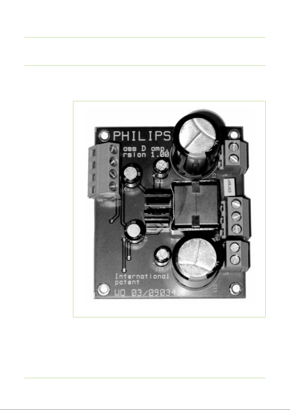
The Universal Class D (UcD) version 1.00 demonstrator board implements a 200 W true
RMS (into a 4 Ω load) high quality audio power amplifier on a very compact printed-circuit
board. The amplifier is built-up of discrete components only, and makes use of Philips
patent WO 03/090343.
UM10155
Discrete Class D High Power Audio Amplifier
001aaf148
Fig 1. General view
The demonstrator board is intended to illustrate the capability of Philips PowerMOSFETs
in discrete high-end PWM audio amplifier applications. The board is self-contained and
only requires a simple (non-stabilized) dual power supply, an audio source (e.g. function
generator,CD player) and a loudspeaker to demonstrate its capabilities. For evaluation at
high output power a provision is made to attach an appropriate heatsink to the MOSFETs
on the board.
UM10155_2 © Koninklijke Philips Electronics N.V. 2006. All rights reserved.
User manual Rev. 02 — 5 September 2006 3 of 12
Page 4
UM10155_2 © Koninklijke Philips Electronics N.V. 2006. All rights reserved.
User manual Rev. 02 — 5 September 2006 4 of 12
xxxx xxxxxxxxxxxxxxxxxxxxxxxxxxxxxx x xxxxxxxxxxxxxx xxxxxxxxxx xxx xxxxxx xxxxxxxxxxxxxxxxxxxxxxx xxxxxxxxxxxxxxxxxxxxxx
xxxxx xxxxxx xx xxxxxxxxxxxxxxxxxxxxxxxxxxxxx xxxxxxxxxxxxxxxxxxxxxx xxxxxxxxxxx xxxxxxx xxxxxxxxxxxxxxxxxxx
xxxxxxxxxxxxxxxx xxxxxxxxxxxxxx xxxxxx xx xxxxxxxxxxxxxxxxxxxxxxxxxxxxxxxx xxxxxxxxxxxxxxxxxxxxxxxx xxxxxxx
xxxxxxxxxxxxxxxxxxxxxxxxxxxxxxxxxxxxxxxxxxxxxx xxxxxxxxxxx xxxxx x x
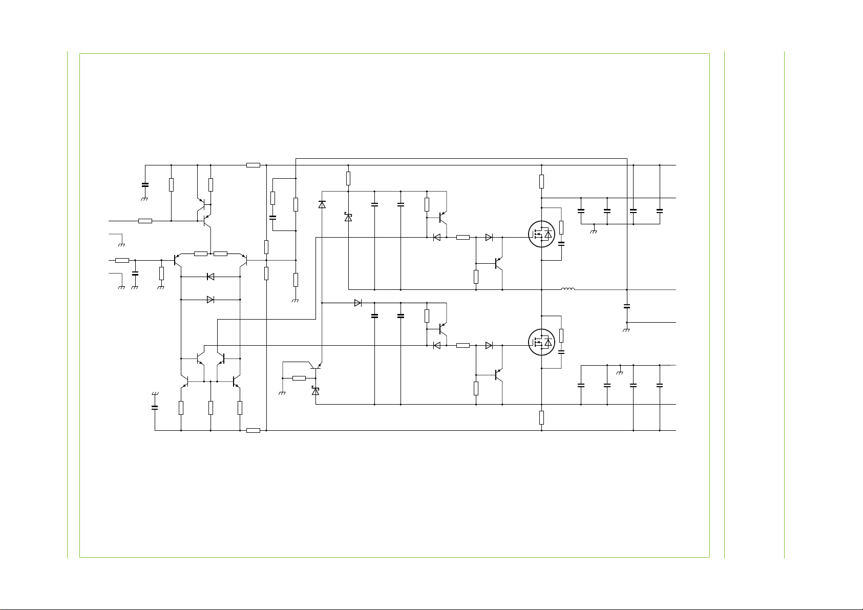
2. Circuit diagram
Philips Semiconductors
R29
10 Ω
R6
C2
47 kΩ
100 nF
R2
1 kΩ
C3
100 nF
BC857
BF821
Q1
Q5
R1
560 Ω
R5
47 kΩ
C1
4.7 nF
J3
J4
J1
J2
Q3
BF820
BC847
R8
220 Ω
Q4
BF721
R3
47 Ω
D1
1PS76SB10
D2
1PS76SB10
Q7
R7
220 Ω
R4
47 Ω
Q8
R9
330 Ω
BF820
BC847
BF821
R13
2.2 kΩ
R12
22 kΩ
C4
220 pF
R14
5.6 MΩ
Q2
Q6
R10
220 Ω
R28
10 Ω
R15
3.9 MΩ
R27
8.2 kΩ
R11
1 kΩ
Q15
D6
BAS321
BF720
D5
PDZ12B
R16
4.7 kΩ
D8
PDZ12B
D7
BAS321
C5
100 µF
C7
100 µF
C6
100 nF
C8
100 nF
R18
390 Ω
D9
1PS76SB10
R17
390 Ω
D10
1PS76SB10
Q10
BC857
Q9
BC857
R20
27 Ω
R19
27 Ω
D11
BAS316
R8
1 kΩ
D12
BAS316
R21
1 kΩ
PHP18NQ11T
Q12
PBSS5140T
PHP18NQ11T
Q11
PBSS5140T
Q14
Q13
R26
0.05 Ω
R25
0.05 Ω
R24
10 Ω
L1
28 µH
R23
10 Ω
C9
100 pF
C10
100 pF
C12
100 nF
C13
100 nF
C11
22 µF
C14
22 µF
C16
100 nF
C15
680 nF
C18
100 nF
C17
1000 µF
C19
1000 µF
001aaf149
J5
J6
J10
J11
Discrete Class D High Power Audio Amplifier
J7
J8
J9
Fig 2. Circuit diagram
UM10155
Page 5
Philips Semiconductors
Table 1. Connections
Connector Function Remarks
J1 audio in - signal use together with J2
J2 audio in - ground use together with J1
J3 amplifier enable whenconnected to ground (J4)
J4 ground use together with J3
J5 positive supply voltage 30 V to 45 V (no need for a
J6 positive current sense can optionally be used in an
J7 power supply ground 0 V
J8 negative current sense can optionally be used in an
J9 negative supply voltage −30 V to −45 V (no need for a
J10 loudspeaker output use together with J11
J11 loudspeaker ground use together with J10
UM10155
Discrete Class D High Power Audio Amplifier
the amplifier is enabled
stabilized power supply)
overcurrent protection scheme
overcurrent protection scheme
stabilized power supply)
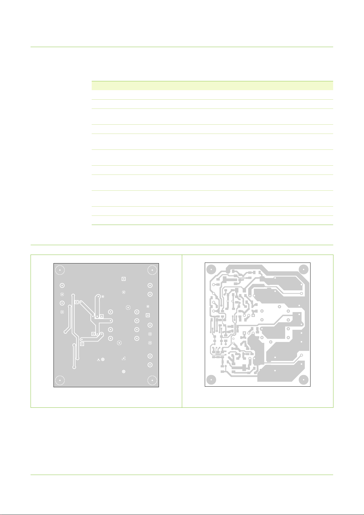
3. Printed-circuit board layout
001aaf150
Fig 3. Top copper layout Fig 4. Bottom copper layout
001aaf151
UM10155_2 © Koninklijke Philips Electronics N.V. 2006. All rights reserved.
User manual Rev. 02 — 5 September 2006 5 of 12
Page 6
Philips Semiconductors
UM10155
Discrete Class D High Power Audio Amplifier
PHILIPS
class D amp.
version 1.00
J3
J4
+
J1
C5
J2
C7
international
patent
WO 03/090343
001aaf152
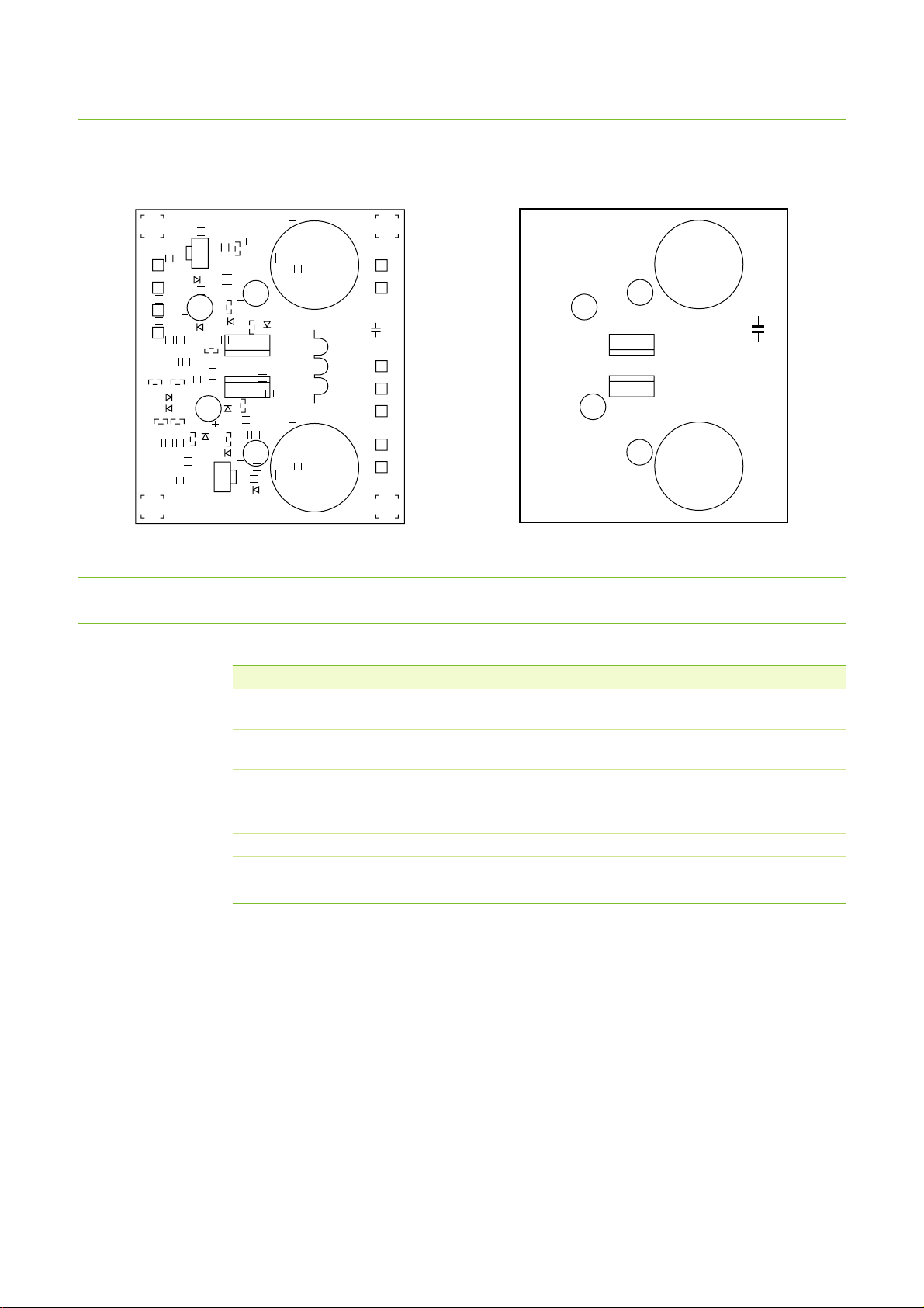
Fig 5. Component layout Fig 6. Top silk-screen
4. Specifications
Table 2. Specifications
Symbol Parameter Conditions Value
V
P
P
L
η efficiency P
THD+N total harmonic
S/N signal-to-noise ratio > 120 dB
f
PWM
V
offset
supply voltage equal positive and negative
supply voltages
output power VP= ±45 V; RL=4Ω;
appropriate heatsink needed
= 100 W; RL=4Ω >92%
L
= 10 W; frequency range
P
L
distortion-plus-noise
from 20 Hz to 20 kHz
PWM frequency idle ~ 400 kHz
offset voltage DC value < 50 mV
+
J5
+
C11
L1
Q14
Q13
+
+
C14
+
C17
C19
J6
C15
J10
J11
J7
J8
J9
001aaf153
±30 V to ±45 V
200 W (RMS)
< 0.03 %
4.1 Pop-less/click-less start-up and shutdown
A provision has been added to the circuit to provide pop-less/click-less start-up and
shutdown. To make use of the start-up facility, make sure that the supply power (pins J5
and J9) is applied prior to enabling the amplifier (connecting J3 to J4). Tobenefit from the
pop-less shutdown feature, disable the amplifier (disconnect J3 and J4) prior to removing
the supply power.
4.2 Overcurrent protection
A provision has been added to the circuit to monitor the current flowing through the Power
MOSFETs (Q13 and Q14). The voltage appearing between pins J5 and J6 is proportional
to the current in MOSFET Q14 (ratio: 50 mV/A) and the voltage between J8 and J9 is
proportional to the current in MOSFET Q13 (ratio: 50 mV/A). With the use of an external
UM10155_2 © Koninklijke Philips Electronics N.V. 2006. All rights reserved.
User manual Rev. 02 — 5 September 2006 6 of 12
Page 7
Philips Semiconductors
circuit these two signals may be used to disable the amplifier (disconnect J3 and J4) in
case of an overcurrent situation. Similarly the J3-J4 pin combination can be used to
disable the amplifier in case of other fault conditions.
4.3 Important notice
The ‘High Power Class D Audio Amplifier Demonstrator Board’ is meant to demonstrate
the capabilities of the specific Class D Amplifier design and its semiconductor
components. No provisions for short-circuit and overcurrent protection were made on the
demonstrator board itself. Neither was an operating temperature compensation feature
implemented on the board. The circuit on the board is reduced to its essentials.
In this implementation the ‘High Power Class D Audio Amplifier Demonstrator Board’ is
not intended to be used for long term operation or under extreme temperature conditions
when delivering substantial output power.
5. Wiring diagram and powering-up
UM10155
Discrete Class D High Power Audio Amplifier
J3
J4
J1
signal
J2
ground
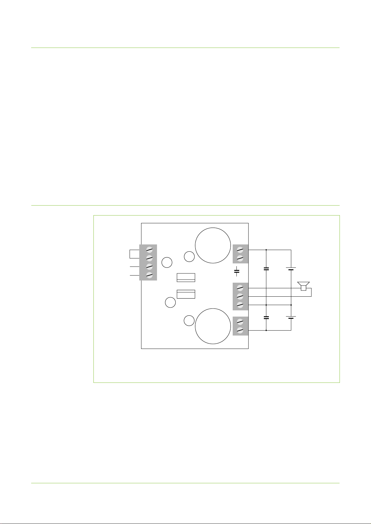
Audio input: J1 is signal; J2 is ground
Initially, leave J6 and J8 unconnected; J7 and J11 are at the same (ground) potential
Fig 7. Wiring diagram
PHILIPS
class D amp.
version 1.00
+
C5
+
C7
international
patent
WO 03/090343
Q13
+
+
C11
C14
Q14
+
J5
J6
C17
10 mF 30 V to 45 V
C15
L1
+
C19
J10
J11
J7
J8
J9
10 mF 30 V to 45 V
4 Ω to 8 Ω
001aaf154
UM10155_2 © Koninklijke Philips Electronics N.V. 2006. All rights reserved.
User manual Rev. 02 — 5 September 2006 7 of 12
Page 8
Philips Semiconductors
6. Adding external features
6.1 Electronic enabling/disabling of the amplifier
UM10155
Discrete Class D High Power Audio Amplifier
PHILIPS
class D amp.
version 1.00
+
C5
C7
international
patent
WO 03/090343
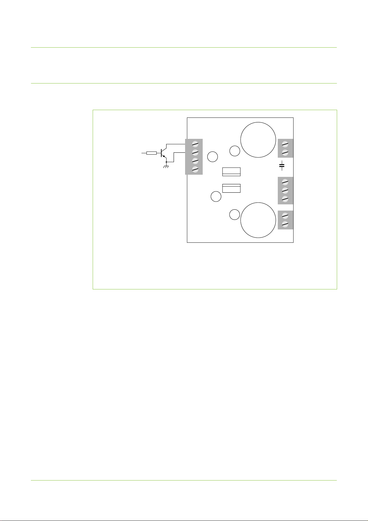
enable
signal
J3
J4
J1
J2
Enable signal:
(HIGH = enable)
(LOW = disable)
Fig 8. Enabling/disabling of the amplifier
Electronic enabling/disabling can be used for:
+
J5
+
C11
L1
Q14
Q13
+
+
C14
+
C17
C19
001aaf155
J6
C15
J10
J11
J7
J8
J9
• Implementing pop-less and click-less start-up and shut-down
• Shutting down the amplifier in case of a failure condition
(short-circuit/overcurrent/over-temperature)
The transistor in the enabling/disabling circuit must be low current, 60 V type (such as
BC846) and the resistor must limit the base current of the transistor to approximately
1 mA (in case of logic level driving, that would mean R = 4.7 kΩ).
UM10155_2 © Koninklijke Philips Electronics N.V. 2006. All rights reserved.
User manual Rev. 02 — 5 September 2006 8 of 12
Page 9
Philips Semiconductors
6.2 Short-circuit and overcurrent protection
UM10155
Discrete Class D High Power Audio Amplifier
Q14
+
J5
J6
C17
C15
L1
+
C19
J10
J11
J7
J8
J9
PHILIPS
class D amp.
J3
J4
J1
J2
version 1.00
+
C5
+
C7
international
patent
WO 03/090343
Q13
+
+
C11
C14
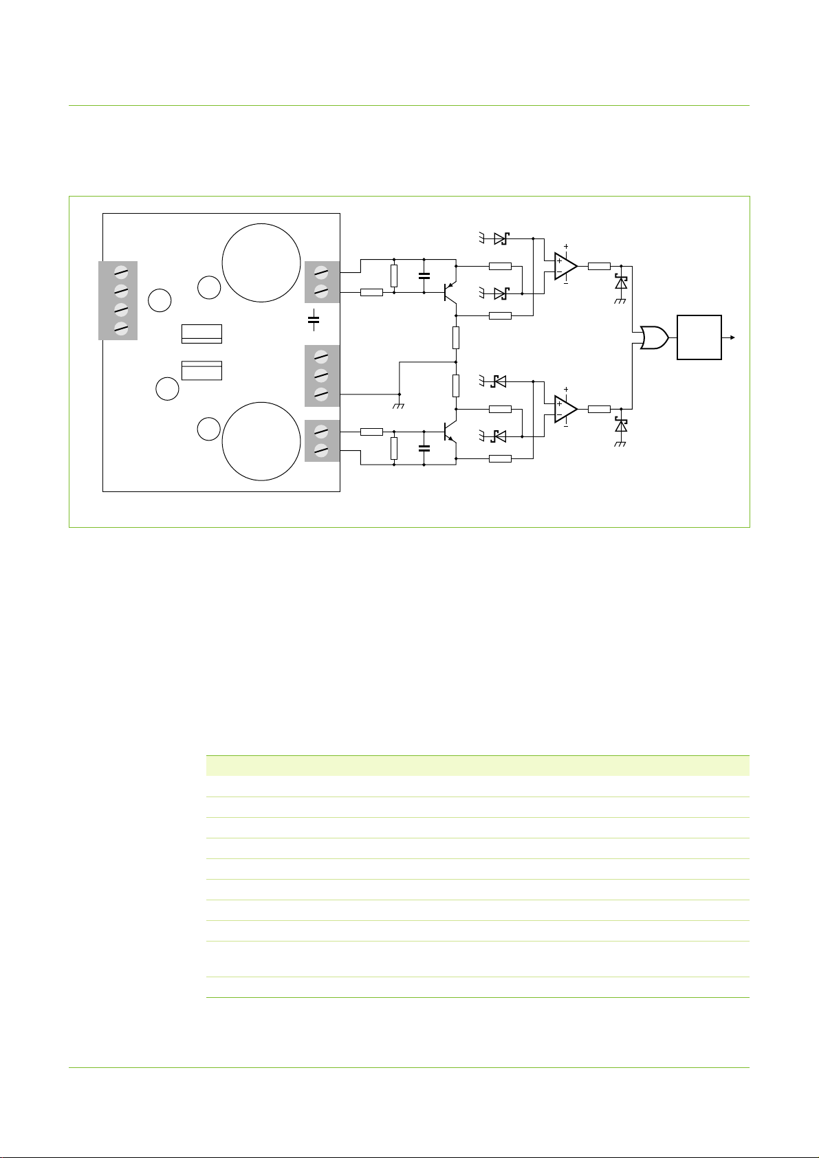
Fig 9. Short-circuit and overcurrent protection
The ‘Short-circuit and overcurrent protection’ circuit must be used together with the
‘Electronic enabling/disabling’ circuit.
The output pins of IC1 and IC2 produce a HIGH logic level pulse when overcurrent is
detected in either the low side MOSFET (Q13 on the Demonstrator Board) and high side
MOSFET (Q14 on the Demonstrator Board) respectively. The two signals are combined
through the IC3 OR-gate. The resulting signal must be processed in the ‘µP or other logic’
block. One of the simplest solutions would be a latch circuit, which on a high pulse forces
the output go low. This causes the ‘Electronic enabling/disabling circuit’ to disable the
amplifier. Through manual intervention and/or after a certain while, the latch should be
reset to a HIGH logic level, which in turn re-enables the amplifier.
D5
R10
C2
R3
R4
R1
R2 C1
Q2
Q1
D4
R11
R6
D2
R5
R7
D1
R8
IC2
IC1
R12
R9
D6
IC3
µP OR
OTHER
LOGIC
to enabling/
disabling circuit
D3
001aaf156
Table 3. Components
Component Value
R1, R4 270 Ω
R2, R3 4.7 kΩ
R5, R6, R7, R8, R9, R10, R11, R12 10 kΩ
C1, C2 4.7 nF
D1, D5 Philips PDZ10B
D2, D3, D4, D6 Philips PDZ5.1B
Q1 Philips BC846
Q2 Philips BC856
IC1, IC2 Fast operational amplifier; feed with +12 V and
−12 V supplies
IC3 Philips HEF4071; feed with 5 V
UM10155_2 © Koninklijke Philips Electronics N.V. 2006. All rights reserved.
User manual Rev. 02 — 5 September 2006 9 of 12
Page 10

Philips Semiconductors
6.3 Sonic performance versus Efficiency trade-off
The dead-time that is allowed between Q13 and Q14 conduction determines the
efficiency of the Demonstrator Board for a great deal; a long dead-time leads to better
efficiency. On the other side,long dead-time also leads to worse sonic performance; it has
important adverse consequences for e.g. THD.
Short dead-time causes quiescent current to go up, thus reducing efficiency and
improving sonic performance. The higher quiescent current is the result of more
cross-conduction of Q13 and Q14. So, most of the power that is lost in this way is
dissipated in Q13 and Q14, which may heat-up excessively. This may cause thermally
instable behavior of the MOSFETs. For that reason, the Demonstrator Board is shipped in
low quiescent current mode – during initial evaluation the risk of damaging the MOSFETs
through thermal runaway is thus reduced.
Nevertheless, by modifying one resistor value, the dead-time can be shortened and
evaluation in enhanced sonic performance mode can take place. Changing R9 to a lower
value decreases dead-time. It is left the responsibility of the experimenter to prevent
thermal runaway, but assistance from Philips will be available through the local sales
representatives.
UM10155
Discrete Class D High Power Audio Amplifier
To reduce the risk of thermal runaway in the enhanced sonic performance mode, a
thermal feedback loop can be implemented: the operating temperature of the MOSFETs
can be fed-back to the dead-time control by changing the fixed R9 value, mounting a PTC
resistor on the heatsink of the MOSFETs and connecting the PTC in parallel with R9.
Again, any changes are left the responsibility of the experimenter, but assistance from
Philips will be available through the local sales representatives.
UM10155_2 © Koninklijke Philips Electronics N.V. 2006. All rights reserved.
User manual Rev. 02 — 5 September 2006 10 of 12
Page 11

Philips Semiconductors
7. Legal information
UM10155
Discrete Class D High Power Audio Amplifier
7.1 Definitions
Draft — The document is a draft version only. The content is still under
internal review and subject to formal approval, which may result in
modifications or additions. Philips Semiconductors does not give any
representations or warranties as to the accuracy or completeness of
information includedherein and shallhave noliabilityfor theconsequences of
use of such information.
7.2 Disclaimers
General — Information in this document is believed to be accurate and
reliable. However, Philips Semiconductors does not give any representations
or warranties, expressed or implied, as to the accuracy or completeness of
such information and shall have no liability for the consequences of use of
such information.
Right to make changes — Philips Semiconductors reserves the right to
make changes to information published in this document, including without
limitation specifications and product descriptions, at any time and without
notice. This document supersedes and replaces all information supplied prior
to the publication hereof.
Suitability for use — Philips Semiconductors products are not designed,
authorized or warranted to be suitable for use in medical, military, aircraft,
space or life support equipment, nor in applications where failure or
malfunction of a Philips Semiconductors product can reasonably be expected
to result in personal injury, death or severe property or environmental
damage. Philips Semiconductors accepts no liability for inclusion and/or use
of Philips Semiconductors products in such equipment or applications and
therefore such inclusion and/or use is at the customer’s own risk.
Applications — Applications that are described herein for any of these
products are for illustrative purposes only. Philips Semiconductors makes no
representation or warranty that such applications will be suitable for the
specified use without further testing or modification.
7.3 Patents
Notice is herewith given that the subject device uses one or more of the
following patents and that each of these patents may have corresponding
patents in other jurisdictions.
WO 03/090343 — owned by Koninklijke Philips Electronics N.V. (int. patent
application)
7.4 Trademarks
Notice: All referenced brands, product names, service names and trademarks
are the property of their respective owners.
UM10155_2 © Koninklijke Philips Electronics N.V. 2006. All rights reserved.
User manual Rev. 02 — 5 September 2006 11 of 12
Page 12

Philips Semiconductors
8. Contents
1 Introduction . . . . . . . . . . . . . . . . . . . . . . . . . . . . 3
2 Circuit diagram. . . . . . . . . . . . . . . . . . . . . . . . . . 4
3 Printed-circuit board layout . . . . . . . . . . . . . . . 5
4 Specifications. . . . . . . . . . . . . . . . . . . . . . . . . . . 6
4.1 Pop-less/click-less start-up and shutdown . . . . 6
4.2 Overcurrent protection . . . . . . . . . . . . . . . . . . . 6
4.3 Important notice . . . . . . . . . . . . . . . . . . . . . . . . 7
5 Wiring diagram and powering-up. . . . . . . . . . . 7
6 Adding external features. . . . . . . . . . . . . . . . . . 8
6.1 Electronic enabling/disabling of the amplifier . . 8
6.2 Short-circuit and overcurrent protection . . . . . . 9
6.3 Sonic performance versus Efficiency trade-off 10
7 Legal information. . . . . . . . . . . . . . . . . . . . . . . 11
7.1 Definitions. . . . . . . . . . . . . . . . . . . . . . . . . . . . 11
7.2 Disclaimers . . . . . . . . . . . . . . . . . . . . . . . . . . . 11
7.3 Patents . . . . . . . . . . . . . . . . . . . . . . . . . . . . . . 11
7.4 Trademarks. . . . . . . . . . . . . . . . . . . . . . . . . . . 11
8 Contents . . . . . . . . . . . . . . . . . . . . . . . . . . . . . . 12
UM10155
Discrete Class D High Power Audio Amplifier
Please be aware that important notices concerning this document and the product(s)
described herein, have been included in section ‘Legal information’.
© Koninklijke Philips Electronics N.V. 2006. All rights reserved.
For more information, please visit: http://www.semiconductors.philips.com.
For sales office addresses, email to: [email protected].
Date of release: 5 September 2006
Document identifier: UM10155_2
 Loading...