

Page 1

PNX2000 User Manual
UM10105_1
Audio Video Input Processor
Rev. 1.0 — 28 November 2003
Page 2

Philips Semiconductors
PNX2000
Audio Video Input Processor
UM10105_1 © Koninklijke Philips Electronics N.V. 2003. All rights reserved.
Rev. 1.0 — 28 November 2003 -ii
Page 3

Philips Semiconductors
Table of Contents
Chapter 1: Functional Specification
PNX2000
Audio Video Input Processor
1.1 Introduction . . . . . . . . . . . . . . . . . . . . . . . . . . . . . 1-1
1.2 PNX2000 Feature Summary . . . . . . . . . . . . . 1-1
1.2.1 Video Features . . . . . . . . . . . . . . . . . . . . . . . . . . . 1-1
1.2.1.1 1FH Video . . . . . . . . . . . . . . . . . . . . . . . . . . . . . . . 1-1
1.2.1.2 2FH Video . . . . . . . . . . . . . . . . . . . . . . . . . . . . . . . 1-1
1.2.1.3 VBI Data Capture . . . . . . . . . . . . . . . . . . . . . . . . . 1-1
1.2.1.4 ITU656 output interface . . . . . . . . . . . . . . . . . . . . 1-2
1.2.2 Audio Features . . . . . . . . . . . . . . . . . . . . . . . . . . . 1-2
1.2.2.1 Demodulator and decoder . . . . . . . . . . . . . . . . . 1-2
Chapter 2: Control Interface
2.1 PNX2000 Control Interface . . . . . . . . . . . . . . 2-1
2.2 I2C Bus Interface . . . . . . . . . . . . . . . . . . . . . . . . 2-2
2.2.1 I2C Bus Features . . . . . . . . . . . . . . . . . . . . . . . . . 2-2
2.2.2 Allocated I2C Address . . . . . . . . . . . . . . . . . . . . . 2-2
2.2.3 I2C Register Access Protocol. . . . . . . . . . . . . . . 2-2
2.2.4 I2C Interface Block . . . . . . . . . . . . . . . . . . . . . . . . 2-6
2.3 BCU Module. . . . . . . . . . . . . . . . . . . . . . . . . . . . . 2-7
2.3.1 BCU Features . . . . . . . . . . . . . . . . . . . . . . . . . . . . 2-7
2.3.2 Registers . . . . . . . . . . . . . . . . . . . . . . . . . . . . . . . . 2-7
2.3.2.1 BCU Interrupt Status Register
(BCU_INT_STATUS). . . . . . . . . . . . . . . . . . . . . . 2-8
2.3.2.2 BCU Interrupt Enable Register
(BCU_INT_ENABLE)
. . . . . . . . . . . . . . . . . . . . . . 2-8
1.2.2.2 Audio Multi Channel Decoder . . . . . . . . . . . . . . . 1-3
1.2.2.3 Volume and tone control . . . . . . . . . . . . . . . . . . . 1-3
1.2.2.4 Reflection and delay . . . . . . . . . . . . . . . . . . . . . . . 1-3
1.2.2.5 Psychoacoustic spatial algorithms,
downmix and split . . . . . . . . . . . . . . . . . . . . . . . . . 1-3
1.2.2.6 Interfaces and switching . . . . . . . . . . . . . . . . . . . 1-4
1.3 Functional Description. . . . . . . . . . . . . . . . . . . 1-4
1.4 Overview of Functional Partitioning . . . . . 1-6
2.3.2.3 BCU Interrupt Status Set Command
(BCU_INT_SET) . . . . . . . . . . . . . . . . . . . . . . . . . . 2-9
2.3.2.4 BCU Interrupt Status Clear Command
(BCU_INT_CLEAR)
2.3.2.5 BCU Bus Fault Status Register
(BCU_FAULT_STATUS) . . . . . . . . . . . . . . . . . . 2-10
2.3.2.6 BCU Bus Fault Address Register
(BCU_FAULT_ADDR) . . . . . . . . . . . . . . . . . . . . 2-10
2.3.2.7 BCU Time-Out Register (BCU_TOUT) . . . . . . 2-11
2.3.2.8 BCU Memory Coherency Register
(BCU_SNOOP) . . . . . . . . . . . . . . . . . . . . . . . . . . 2-11
. . . . . . . . . . . . . . . . . . . . . . . 2-9
2.4 Memory Map . . . . . . . . . . . . . . . . . . . . . . . . . . . . 2-12
Chapter 3: I2D
3.1 Introduction . . . . . . . . . . . . . . . . . . . . . . . . . . . . . 3-1
3.2 Functional Capabilities of the Links. . . . . 3-2
3.3 Transmitter . . . . . . . . . . . . . . . . . . . . . . . . . . . . . . 3-3
3.4 Receiver . . . . . . . . . . . . . . . . . . . . . . . . . . . . . . . . . 3-4
3.4.1 Transmitter / Receiver Transmission Modes. . 3-6
3.4.2 Data Rate and Timing Output Signals . . . . . . . 3-8
3.5 Configuration Registers. . . . . . . . . . . . . . . . . 3-9
3.5.1 I2D Register Map . . . . . . . . . . . . . . . . . . . . . . . . 3-10
3.5.1.1 I2D_RX_CTRL . . . . . . . . . . . . . . . . . . . . . . . . . . 3-10
3.5.1.2 I2D_RX_STATUS. . . . . . . . . . . . . . . . . . . . . . . . 3-11
3.5.1.3 I2D_REC_DEMUX_MODE. . . . . . . . . . . . . . . . 3-11
3.5.1.4 I2D _REC_SYNC_LOST. . . . . . . . . . . . . . . . . . 3-12
3.5.1.5 I2D _PRBS_STAT . . . . . . . . . . . . . . . . . . . . . . . 3-13
3.5.1.6 I2D _PRBS_CTRL . . . . . . . . . . . . . . . . . . . . . . . 3-13
3.5.1.7 I2D _INT_STATUS. . . . . . . . . . . . . . . . . . . . . . . 3-14
Chapter 4: Video Processing (Viddec)
4.1 Overview. . . . . . . . . . . . . . . . . . . . . . . . . . . . . . . . . 4-1
4.2 Data input, Sample Rate Converter
and timing
4.2.1 Short Description . . . . . . . . . . . . . . . . . . . . . . . . . 4-3
4.3 AGC. . . . . . . . . . . . . . . . . . . . . . . . . . . . . . . . . . . . . . 4-5
4.3.1 Short Description . . . . . . . . . . . . . . . . . . . . . . . . . 4-5
4.3.2 AGC Gain Stages . . . . . . . . . . . . . . . . . . . . . . . . . 4-6
. . . . . . . . . . . . . . . . . . . . . . . . . . . . . . . 4-3
3.5.1.8 I2D _INT_ENABLE . . . . . . . . . . . . . . . . . . . . . . . 3-14
3.5.1.9 I2D _INT_CLEAR . . . . . . . . . . . . . . . . . . . . . . . . 3-15
3.5.1.10 I2D _INT_SET . . . . . . . . . . . . . . . . . . . . . . . . . . . 3-15
3.5.1.11 I2D _MOD_ID . . . . . . . . . . . . . . . . . . . . . . . . . . . 3-16
3.6 Interrupt Procedure. . . . . . . . . . . . . . . . . . . . 3-16
3.6.1 Interrupt Behaviour . . . . . . . . . . . . . . . . . . . . . . . 3-16
3.6.2 Software Action with Registers. . . . . . . . . . . . . 3-17
3.6.2.1 Start Up. . . . . . . . . . . . . . . . . . . . . . . . . . . . . . . . . 3-17
3.6.2.2 Normal Operation . . . . . . . . . . . . . . . . . . . . . . . . 3-18
3.6.2.3 Soft_reset . . . . . . . . . . . . . . . . . . . . . . . . . . . . . . . 3-18
3.6.2.4 Change of Source Selection . . . . . . . . . . . . . . . 3-18
3.6.2.5 Sync lost on a datalink (Out Of Sync) . . . . . . . 3-18
3.6.2.6 Missing data_valid pulses . . . . . . . . . . . . . . . . . 3-19
3.6.2.7 Test mode. . . . . . . . . . . . . . . . . . . . . . . . . . . . . . . 3-20
4.3.3 AGC Control Circuit . . . . . . . . . . . . . . . . . . . . . . 4-11
4.3.3.1 AGC Control Circuit for CVBS / Yyc path. . . . 4-11
4.3.3.2 AGC Control Circuit for Yyuv / Cyc Path . . . . 4-14
4.3.3.3 AGC Control Circuit for the Sync Path . . . . . . 4-22
4.4 Digital Multi Standard Decoder
(DMSD)
4.4.1 Y processing . . . . . . . . . . . . . . . . . . . . . . . . . . . . 4-25
. . . . . . . . . . . . . . . . . . . . . . . . . . . . . . . . . . 4-23
UM10105_1 © Koninklijke Philips Electronics N.V. 2003. All rights reserved.
Rev. 1.0 — 28 November 2003 -iii
Page 4

Philips Semiconductors
PNX2000
Audio Video Input Processor
4.4.2 Demodulator, Filtering (Combfilter)
and SECAM Decoder
4.4.2.1 Demodulator . . . . . . . . . . . . . . . . . . . . . . . . . . . . 4-28
4.4.2.2 Filtering. . . . . . . . . . . . . . . . . . . . . . . . . . . . . . . . . 4-29
4.4.2.3 SECAM decoder . . . . . . . . . . . . . . . . . . . . . . . . . 4-32
4.4.3 Color PLL and Delay Line . . . . . . . . . . . . . . . . . 4-33
4.4.3.1 Color PLL . . . . . . . . . . . . . . . . . . . . . . . . . . . . . . . 4-33
4.4.4 Color System Manager . . . . . . . . . . . . . . . . . . . 4-38
4.4.5 Signal controls, Macrovision and Debug . . . . 4-46
4.4.5.1 Signal Controls . . . . . . . . . . . . . . . . . . . . . . . . . . 4-46
4.4.5.2 Macrovision . . . . . . . . . . . . . . . . . . . . . . . . . . . . . 4-47
4.4.5.3 Debug & Control . . . . . . . . . . . . . . . . . . . . . . . . . 4-49
4.4.6 Sync Processing . . . . . . . . . . . . . . . . . . . . . . . . . 4-50
4.4.6.1 Horizontal Sync Processing 1 Fh
and Measurement/Control
. . . . . . . . . . . . . . . . . . . . 4-27
. . . . . . . . . . . . . . . . 4-52
Chapter 5: Data Capture Unit
5.1 Summary of Functions . . . . . . . . . . . . . . . . . . 5-1
5.2 Block Diagram . . . . . . . . . . . . . . . . . . . . . . . . . . . 5-2
5.2.1 Block Description . . . . . . . . . . . . . . . . . . . . . . . . . 5-2
5.3 Design Specification. . . . . . . . . . . . . . . . . . . . . 5-3
5.4 Data Packet Formats . . . . . . . . . . . . . . . . . . . . 5-3
5.4.1 Status Bytes . . . . . . . . . . . . . . . . . . . . . . . . . . . . . 5-4
5.4.2 Euro WST, US WST and NABTS Data . . . . . . 5-4
5.4.3 WSS625 Data . . . . . . . . . . . . . . . . . . . . . . . . . . . . 5-4
5.4.4 WSS525 Data . . . . . . . . . . . . . . . . . . . . . . . . . . . . 5-5
5.4.5 VPS Data . . . . . . . . . . . . . . . . . . . . . . . . . . . . . . . . 5-5
5.4.6 Closed Caption . . . . . . . . . . . . . . . . . . . . . . . . . . . 5-6
5.4.7 Moji (Japanese Text) . . . . . . . . . . . . . . . . . . . . . . 5-6
5.4.8 VITC Data . . . . . . . . . . . . . . . . . . . . . . . . . . . . . . . 5-6
5.4.9 Open Data Types . . . . . . . . . . . . . . . . . . . . . . . . . 5-6
4.4.6.2 Vertical Sync Processing 1 Fh . . . . . . . . . . . . . 4-58
4.4.6.3 Horizontal Sync Processing 2 Fh . . . . . . . . . . . 4-63
4.4.6.4 Vertical Sync Processing 2 Fh . . . . . . . . . . . . . 4-69
4.4.6.5 Fast Blanking / External 2 Fh Sync /
Clamp Info
4.4.6.6 YUV Switch + Formatter . . . . . . . . . . . . . . . . . . 4-78
4.4.7 Switching VIDDEC between 1Fh and 2Fh . . . 4-80
4.4.8 Use of interrupt bits. . . . . . . . . . . . . . . . . . . . . . . 4-81
4.4.9 Automatic selection of different
input signal formats. . . . . . . . . . . . . . . . . . . . . . . 4-82
4.4.9.1 CVBS or Y/C Input Selection . . . . . . . . . . . . . . 4-83
4.4.9.2 CVBS + RGB Insert via SCART. . . . . . . . . . . . 4-86
4.4.9.3 CVI Input Selection . . . . . . . . . . . . . . . . . . . . . . . 4-88
. . . . . . . . . . . . . . . . . . . . . . . . . . . . . . 4-74
5.5 Packet Processing Capabilities. . . . . . . . . . 5-7
5.5.1 Magazine and Packet Number Decoding . . . . . 5-7
5.5.1.1 Input Data Format . . . . . . . . . . . . . . . . . . . . . . . . 5-7
5.5.1.2 Output Data Format . . . . . . . . . . . . . . . . . . . . . . . 5-7
5.5.2 Page Header Decoding . . . . . . . . . . . . . . . . . . . . 5-8
5.5.3 WSS525 CRC Checking . . . . . . . . . . . . . . . . . . . 5-8
5.5.4 Packet Validity Checking. . . . . . . . . . . . . . . . . . . 5-8
5.6 Registers. . . . . . . . . . . . . . . . . . . . . . . . . . . . . . . . . 5-9
5.6.1 DCR1: Data Capture Register (Write) . . . . . . . 5-10
5.6.2 DCR2: Data Capture Register 2 (Write) . . . . . 5-11
5.6.3 LCR2..LCR24: Line Control
Registers (Write) . . . . . . . . . . . . . . . . . . . . . . . . . 5-11
5.6.4 DCS: Data Capture Status (Read). . . . . . . . . . 5-13
5.6.5 Interrupt Registers (Read/Write) . . . . . . . . . . . 5-14
5.6.6 MODULE_ID (Read). . . . . . . . . . . . . . . . . . . . . . 5-14
Chapter 6: ITU656
6.1. ITU656 Formatter Overview . . . . . . . . . . . . . 6-1
6.2. ITU656 Formatter Data Interfaces . . . . . . . 6-2
6.3. Control Registers . . . . . . . . . . . . . . . . . . . . . . . 6-3
6.3.1 ITU656 Formatter Registers . . . . . . . . . . . . . . . . 6-3
6.3.2 CONFIG Register . . . . . . . . . . . . . . . . . . . . . . . . . 6-3
6.3.2.1 MODE . . . . . . . . . . . . . . . . . . . . . . . . . . . . . . . . . . 6-4
6.3.2.2 Columbus. . . . . . . . . . . . . . . . . . . . . . . . . . . . . . . . 6-4
6.3.2.3 VBI_CONTROL. . . . . . . . . . . . . . . . . . . . . . . . . . . 6-5
6.3.2.4 VBI_ONLY . . . . . . . . . . . . . . . . . . . . . . . . . . . . . . . 6-6
6.3.2.5 CVBS_COMPL . . . . . . . . . . . . . . . . . . . . . . . . . . . 6-6
6.3.2.6 UV_COMPL. . . . . . . . . . . . . . . . . . . . . . . . . . . . . . 6-6
6.3.2.7 DITHER . . . . . . . . . . . . . . . . . . . . . . . . . . . . . . . . . 6-6
6.3.2.8 DC_JUSTIFIED. . . . . . . . . . . . . . . . . . . . . . . . . . . 6-7
6.3.2.9 CLOCK_INVERT . . . . . . . . . . . . . . . . . . . . . . . . . 6-7
6.3.2.10 CLOCK_STUTTER . . . . . . . . . . . . . . . . . . . . . . . 6-8
6.3.2.11 PROGRESSIVE_MODE . . . . . . . . . . . . . . . . . . . 6-8
6.3.2.12 OUTPUT_TEST_MODE . . . . . . . . . . . . . . . . . . . 6-8
6.3.2.13 INPUT_TEST_MODE . . . . . . . . . . . . . . . . . . . . . 6-9
6.3.2.14 DVO_ENABLE . . . . . . . . . . . . . . . . . . . . . . . . . . . 6-9
6.3.3 Data Identification Register – VBI data. . . . . . . 6-9
6.3.4 Data Identification Register – HBI data . . . . . 6-10
6.3.5 CAPTURE Register . . . . . . . . . . . . . . . . . . . . . 6-10
UM10105_1 © Koninklijke Philips Electronics N.V. 2003. All rights reserved.
Rev. 1.0 — 28 November 2003 -iv
6.3.6 FIFO Register . . . . . . . . . . . . . . . . . . . . . . . . . . . 6-11
6.3.7 VF CONTROL Register . . . . . . . . . . . . . . . . . . . 6-11
6.3.8 VF SYNC Register . . . . . . . . . . . . . . . . . . . . . . . 6-11
6.3.9 FIELD 1 Register. . . . . . . . . . . . . . . . . . . . . . . . . 6-12
6.3.10 FIELD 2 Register. . . . . . . . . . . . . . . . . . . . . . . . . 6-12
6.3.11 VBI 1 Register . . . . . . . . . . . . . . . . . . . . . . . . . . . 6-12
6.3.12 VBI 2 Register . . . . . . . . . . . . . . . . . . . . . . . . . . . 6-13
6.3.13 VBI 3 Register . . . . . . . . . . . . . . . . . . . . . . . . . . . 6-13
6.3.14 VBI 4 Register . . . . . . . . . . . . . . . . . . . . . . . . . . . 6-13
6.3.15 PROG HBI Register . . . . . . . . . . . . . . . . . . . . . . 6-13
6.3.16 YUV Offset Register . . . . . . . . . . . . . . . . . . . . . . 6-14
6.3.17 Interrupt Registers . . . . . . . . . . . . . . . . . . . . . . . 6-14
6.3.17.1 INT_STATUS Register . . . . . . . . . . . . . . . . . . . 6-14
6.3.17.2 INT_ENABLE Register . . . . . . . . . . . . . . . . . . . 6-15
6.3.17.3 INT_CLEAR Register . . . . . . . . . . . . . . . . . . . . 6-15
6.3.17.4 INT_SET Register . . . . . . . . . . . . . . . . . . . . . . . 6-15
6.3.18 MODULE_ID Register . . . . . . . . . . . . . . . . . . . . 6-15
6.3.19 Debug Control Register . . . . . . . . . . . . . . . . . . 6-15
6.4. Video Line Interface Signal Structure. . . 6-17
6.4.1 PNX2000 (Mode 0) in Columbus Mode . . . . . 6-17
6.4.2 PNX2000 (Mode 1) in Columbus Mode . . . . . 6-18
6.4.3 PNX2000 (Mode 0) in PNX8550 mode . . . . . . 6-18
Page 5

Philips Semiconductors
PNX2000
Audio Video Input Processor
6.4.4 PNX2000 (Mode 1) in PNX8550 mode. . . . . . 6-19
6.4.5 PNX2000 (Mode 2) in PNX8550 mode. . . . . . 6-19
Chapter 7: Audio Processing
7.1 General Description . . . . . . . . . . . . . . . . . . . . . 7-1
7.2 Supported Standards . . . . . . . . . . . . . . . . . . . . 7-2
7.2.1 Analogue 2-carrier Systems . . . . . . . . . . . . . . . . 7-3
7.2.2 2-carrier Systems with NICAM . . . . . . . . . . . . . . 7-3
7.2.3 Satellite Systems . . . . . . . . . . . . . . . . . . . . . . . . . 7-4
7.2.4 BTSC/SAP, Japan (EIAJ) and FM Radio
Systems . . . . . . . . . . . . . . . . . . . . . . . . . . . . . . . . . 7-4
7.3 Features . . . . . . . . . . . . . . . . . . . . . . . . . . . . . . . . . 7-4
7.3.1 Demodulator and Decoder . . . . . . . . . . . . . . . . . 7-4
7.3.2 Audio Multi Channel Decoder. . . . . . . . . . . . . . . 7-5
7.3.3 Volume and Tone Control . . . . . . . . . . . . . . . . . . 7-5
7.3.4 Reflection and Delay . . . . . . . . . . . . . . . . . . . . . . 7-6
7.3.5 Psychoacoustic Spatial Algorithms,
Downmix and Split . . . . . . . . . . . . . . . . . . . . . . . . 7-6
7.3.6 Interfaces and Switching . . . . . . . . . . . . . . . . . . . 7-6
7.4 Functional Overview of the
Sound Core
7.5 Sound Core Control Interface . . . . . . . . . . . 7-8
7.6 I2S . . . . . . . . . . . . . . . . . . . . . . . . . . . . . . . . . . . . . . . 7-9
7.7 Digital-Analogue Converters . . . . . . . . . . . 7-11
7.8 Demdec DSP. . . . . . . . . . . . . . . . . . . . . . . . . . . . 7-11
7.8.1 DDEP in Brief . . . . . . . . . . . . . . . . . . . . . . . . . . . 7-12
7.8.2 What DDEP Does NOT Do. . . . . . . . . . . . . . . . 7-13
7.8.3 Design Considerations . . . . . . . . . . . . . . . . . . . 7-14
7.8.4 DDEP Basics and Usage . . . . . . . . . . . . . . . . . 7-15
7.8.5 DEMDEC Hardware Blocks and the
Sample Rate Problem . . . . . . . . . . . . . . . . . . . . 7-15
7.8.6 Signal Processing in DSP Software . . . . . . . . 7-16
7.8.7 SRC constraints . . . . . . . . . . . . . . . . . . . . . . . . . 7-19
7.8.8 The DDEP Control Register . . . . . . . . . . . . . . . 7-23
7.8.8.1 Mode Selection . . . . . . . . . . . . . . . . . . . . . . . . . . 7-23
7.8.8.2 Starting and Restarting . . . . . . . . . . . . . . . . . . . 7-24
7.8.8.3 DDEP Control Variables . . . . . . . . . . . . . . . . . . 7-24
7.8.8.4 Dependencies Between Variables in
the DDEPR
7.8.8.5 Automute Function . . . . . . . . . . . . . . . . . . . . . . . 7-27
7.8.8.6 NICAM Configuration . . . . . . . . . . . . . . . . . . . . . 7-28
7.8.8.7 Amplitude and Noise Threshold Registers. . . 7-30
7.8.8.8 SAP Detection. . . . . . . . . . . . . . . . . . . . . . . . . . . 7-32
7.8.8.9 EIAJ Subcarrier Detection. . . . . . . . . . . . . . . . . 7-32
7.8.9 Other DEMDEC Control Options . . . . . . . . . . . 7-33
7.8.9.1 ADC Channel Control . . . . . . . . . . . . . . . . . . . . 7-36
7.8.10 Status Registers . . . . . . . . . . . . . . . . . . . . . . . . . 7-37
7.8.10.1 DEMDEC Status Register. . . . . . . . . . . . . . . . . 7-37
7.8.10.2 NICAM Status Registers . . . . . . . . . . . . . . . . . . 7-40
7.8.11 Noise Detection. . . . . . . . . . . . . . . . . . . . . . . . . . 7-41
7.8.12 Muting all DEMDEC Outputs . . . . . . . . . . . . . . 7-41
7.8.13 Using DDEP in a Set Design . . . . . . . . . . . . . . 7-42
7.8.13.1 Application Related Constant Settings . . . . . . 7-42
7.8.13.2 Prerequisites and User Interface . . . . . . . . . . . 7-42
7.8.13.3 Auto-tune Process . . . . . . . . . . . . . . . . . . . . . . . 7-44
7.8.13.4 Channel Switch Procedure . . . . . . . . . . . . . . . . 7-44
. . . . . . . . . . . . . . . . . . . . . . . . . . . . . . 7-7
. . . . . . . . . . . . . . . . . . . . . . . . . . . . . 7-27
6.4.6 PNX2000 (Mode 3) in PNX8550 mode . . . . . . 6-19
7.8.14 Details of Operation . . . . . . . . . . . . . . . . . . . . . . 7-45
7.8.14.1 Search Procedures (ASD Mode) . . . . . . . . . . . 7-45
7.8.14.2 Using the SSS Mode . . . . . . . . . . . . . . . . . . . . . 7-52
7.8.14.3 Automatic Signal Switching and Routing . . . . 7-54
7.9 AUDIO-DSP . . . . . . . . . . . . . . . . . . . . . . . . . . . . . 7-59
7.9.1 Functional Overview . . . . . . . . . . . . . . . . . . . . . . 7-59
7.9.2 Loudspeaker Channel Sound Modes . . . . . . . 7-62
7.9.3 Comments about Function Control . . . . . . . . . 7-63
7.9.3.1 Automatic Volume Levelling (AVL) . . . . . . . . . 7-63
7.9.3.2 Virtual Dolby® Surround (VDS). . . . . . . . . . . . . 7-63
7.9.3.3 Virtual Dolby® Digital (VDD) . . . . . . . . . . . . . . . 7-64
7.9.3.4 Noise Sequencer for DPLII . . . . . . . . . . . . . . . . 7-65
7.9.3.5 Dolby® Pro Logic II® Function (DPLII) . . . . . . 7-65
7.9.3.6 Bass / Treble . . . . . . . . . . . . . . . . . . . . . . . . . . . . 7-67
7.9.3.7 Loudness . . . . . . . . . . . . . . . . . . . . . . . . . . . . . . . 7-69
7.9.3.8 Incredible Stereo (IStereo) . . . . . . . . . . . . . . . . 7-70
7.9.3.9 Incredible Mono (IMono) . . . . . . . . . . . . . . . . . . 7-72
7.9.3.10 Dynamic Ultra Bass (DUB) . . . . . . . . . . . . . . . . 7-73
7.9.3.11 Dynamic Bass Enhancement (DBE) . . . . . . . . 7-75
7.9.3.12 BBE
7.9.3.13 Bass Management . . . . . . . . . . . . . . . . . . . . . . . 7-77
7.9.3.14 Acoustical Compensation . . . . . . . . . . . . . . . . . 7-82
7.9.3.15 Equalizers. . . . . . . . . . . . . . . . . . . . . . . . . . . . . . . 7-83
7.9.3.16 Volume and Trim. . . . . . . . . . . . . . . . . . . . . . . . . 7-87
7.9.3.17 Beeper. . . . . . . . . . . . . . . . . . . . . . . . . . . . . . . . . . 7-87
7.9.3.18 Mono Signal for Cancellation in the
7.9.3.19 Audio Monitor. . . . . . . . . . . . . . . . . . . . . . . . . . . . 7-87
7.9.3.20 Digital Output Crossbar . . . . . . . . . . . . . . . . . . . 7-87
7.9.3.21 Clip Management . . . . . . . . . . . . . . . . . . . . . . . . 7-88
7.9.3.22 Power On / Reset Specification . . . . . . . . . . . . 7-89
7.9.4 Audio Feature Specification . . . . . . . . . . . . . . . 7-89
7.9.4.1 Automatic Volume Levelling (AVL) . . . . . . . . . 7-90
7.9.4.2 Dolby® Pro Logic II® (DPLII) . . . . . . . . . . . . . . . 7-91
7.9.4.3 Virtual Dolby® Surround (VDS). . . . . . . . . . . . . 7-92
7.9.4.4 Virtual Dolby® Digital (VDD) . . . . . . . . . . . . . . . 7-93
7.9.4.5 Incredible Stereo (IStereo) . . . . . . . . . . . . . . . . 7-94
7.9.4.6 Incredible Mono (IMono) . . . . . . . . . . . . . . . . . . 7-95
7.9.4.7 Dynamic Ultra Bass (DUB) . . . . . . . . . . . . . . . . 7-96
7.9.4.8 Dynamic Bass Enhancement (DBE) . . . . . . . . 7-97
7.9.4.9 Loudness . . . . . . . . . . . . . . . . . . . . . . . . . . . . . . . 7-98
7.9.4.10 BBE
7.9.4.11 Bass and Treble . . . . . . . . . . . . . . . . . . . . . . . . 7-100
7.9.4.12 Bass Management . . . . . . . . . . . . . . . . . . . . . . 7-101
7.9.4.13 Delay Line Unit . . . . . . . . . . . . . . . . . . . . . . . . . 7-102
7.9.4.14 Pseudo Hall / Matrix . . . . . . . . . . . . . . . . . . . . . 7-103
7.9.4.15 Master Volume & Trim . . . . . . . . . . . . . . . . . . . 7-104
7.9.4.16 Volume and Balance for Auxiliary
7.9.4.17 Level Adjust . . . . . . . . . . . . . . . . . . . . . . . . . . . . 7-106
7.9.4.18 Main Equalizer . . . . . . . . . . . . . . . . . . . . . . . . . . 7-107
7.9.4.19 Central Equalizer. . . . . . . . . . . . . . . . . . . . . . . . 7-108
7.9.4.20 Soft Mute . . . . . . . . . . . . . . . . . . . . . . . . . . . . . . 7-109
. . . . . . . . . . . . . . . . . . . . . . . . . . . . . . . . . . . 7-76
®
Voice Control IC . . . . . . . . . . . . . . . . . . . . . . . . . 7-87
. . . . . . . . . . . . . . . . . . . . . . . . . . . . . . . . . . . 7-99
®
Channels
. . . . . . . . . . . . . . . . . . . . . . . . . . . . . . . 7-105
UM10105_1 © Koninklijke Philips Electronics N.V. 2003. All rights reserved.
Rev. 1.0 — 28 November 2003 -v
Page 6

Philips Semiconductors
PNX2000
Audio Video Input Processor
7.9.4.21 Digital Input Crossbar . . . . . . . . . . . . . . . . . . . 7-110
7.9.4.22 Digital Output Crossbar . . . . . . . . . . . . . . . . . . 7-111
7.9.4.23 Audio Monitor . . . . . . . . . . . . . . . . . . . . . . . . . . 7-112
Chapter 8: CGU
8.1 Clock Generation Unit (CGU) . . . . . . . . . . . . 8-1
8.2 PNX2000 Clock Requirements. . . . . . . . . . . 8-1
8.3 Crystal Oscillator Specification . . . . . . . . . 8-3
8.4 Phase Locked Loops . . . . . . . . . . . . . . . . . . . . 8-4
8.4.1 Power Saving Mode . . . . . . . . . . . . . . . . . . . . . . . 8-6
8.5 ITU Output Clock Generation. . . . . . . . . . . . 8-7
8.6 I2S Word Select (WS) Clock
Generation
. . . . . . . . . . . . . . . . . . . . . . . . . . . . . . . 8-7
8.7 Clock Selection for 1fh and 2fh
Video Modes
. . . . . . . . . . . . . . . . . . . . . . . . . . . 8-11
Chapter 9: Standards, Modes and Settings
9.1 Video Standards . . . . . . . . . . . . . . . . . . . . . . . . . 9-1
9.2 Data Capture Standards . . . . . . . . . . . . . . . . . 9-2
9.3 Audio Standards. . . . . . . . . . . . . . . . . . . . . . . . . 9-3
9.4 Display Modes . . . . . . . . . . . . . . . . . . . . . . . . . . . 9-4
9.5 ITU656 Formatter Settings. . . . . . . . . . . . . . . 9-5
9.6 Viddec Settings. . . . . . . . . . . . . . . . . . . . . . . . . . 9-6
7.9.4.24 Beeper. . . . . . . . . . . . . . . . . . . . . . . . . . . . . . . . . 7-113
7.9.4.25 Noise Generator . . . . . . . . . . . . . . . . . . . . . . . . 7-114
8.8 Clock Configuration and Status
Registers
. . . . . . . . . . . . . . . . . . . . . . . . . . . . . . . . 8-11
8.9 Power-on and Reset . . . . . . . . . . . . . . . . . . . . 8-14
8.9.1 Reset Selection . . . . . . . . . . . . . . . . . . . . . . . . . . 8-14
8.9.2 Reset Operation and Power Management . . . 8-15
8.9.2.1 Power on/External Hard Reset . . . . . . . . . . . . 8-15
8.9.2.2 Soft Resets. . . . . . . . . . . . . . . . . . . . . . . . . . . . . . 8-15
8.10 Interrupts . . . . . . . . . . . . . . . . . . . . . . . . . . . . . . . 8-16
8.10.1 Top-Level Interrupt Status and
Control Registers . . . . . . . . . . . . . . . . . . . . . . . . 8-16
8.11 Miscellaneous Registers. . . . . . . . . . . . . . . . 8-17
9.7 DCU Register Settings . . . . . . . . . . . . . . . . . . . 9-8
9.8 I2D Settings . . . . . . . . . . . . . . . . . . . . . . . . . . . . . . 9-8
9.9 GTU Settings . . . . . . . . . . . . . . . . . . . . . . . . . . . . . 9-9
9.10 BCU Settings. . . . . . . . . . . . . . . . . . . . . . . . . . . . 9-10
9.11 MPIF Settings . . . . . . . . . . . . . . . . . . . . . . . . . . . 9-10
Chapter 10: Device Initialization
10.1 Power-up Sequence (after Power-on
Reset)
. . . . . . . . . . . . . . . . . . . . . . . . . . . . . . . . . . . 10-1
Chapter 11: Application Example
11.1 Application Example
(Single PNX2000)
. . . . . . . . . . . . . . . . . . . . . . . 11-1
Chapter 12: PCB Layout Guidelines
12.1 Introduction . . . . . . . . . . . . . . . . . . . . . . . . . . . . 12-1
12.2 Power Supplies and Grounding . . . . . . . 12-1
12.2.1 PNX2000 . . . . . . . . . . . . . . . . . . . . . . . . . . . . . . . 12-1
12.2.2 PNX3000 . . . . . . . . . . . . . . . . . . . . . . . . . . . . . . . 12-2
Chapter 13: Support Tools
13.1 Universal Register Debugger. . . . . . . . . . . 13-1
List of Figures
Chapter 1: Functional Specification
10.2 Full-power to Standby Sequence . . . . . . . 10-1
10.3 Standby to Full-power Sequence . . . . . . . 10-2
12.3 Signal Pins . . . . . . . . . . . . . . . . . . . . . . . . . . . . . 12-4
12.3.1 Data-Link . . . . . . . . . . . . . . . . . . . . . . . . . . . . . . . 12-4
12.3.2 SAW Filters and IF Leads . . . . . . . . . . . . . . . . . 12-5
12.3.3 DACs Reference Voltages. . . . . . . . . . . . . . . . . 12-6
Figure 1: PNX2000 Block Diagram . . . . . . . . . . . . . . . 1-5
UM10105_1 © Koninklijke Philips Electronics N.V. 2003. All rights reserved.
Rev. 1.0 — 28 November 2003 -vi
Page 7

Philips Semiconductors
Chapter 2: Control Interface
PNX2000
Audio Video Input Processor
Figure 1: Control Interface. . . . . . . . . . . . . . . . . . . . . . . 2-1
Figure 2: Single Write. . . . . . . . . . . . . . . . . . . . . . . . . . . 2-3
Figure 3: Single Read. . . . . . . . . . . . . . . . . . . . . . . . . . . 2-4
Chapter 3: I2D
Figure 1: Overview - I2D Transmitter/Receiver . . . . . 3-2
Figure 2: Overview - Datalink Modes, Transmitter
Side PNX3000 . . . . . . . . . . . . . . . . . . . . . . . . 3-3
Figure 3: Simplified Transmitter Side PNX3000 . . . . 3-4
Figure 4: Simplified Receiver Side PNX2000. . . . . . . 3-6
Chapter 4: Video Processing (Viddec)
Figure 1: Block Diagram VIDeo DECoder . . . . . . . . . 4-2
Figure 2: Input and Sample Rate Conversion . . . . . . 4-3
Figure 3: Selection Input Data Streams for
VIDDEC in I2D . . . . . . . . . . . . . . . . . . . . . . . . 4-4
Figure 4: AGC Block Diagram. . . . . . . . . . . . . . . . . . . . 4-5
Figure 5: AGC Gain Stages. . . . . . . . . . . . . . . . . . . . . . 4-6
Figure 6: Input Format vs. Output Format of AGC . . 4-7
Figure 7: AGC Universal Programmable
Gain Stage. . . . . . . . . . . . . . . . . . . . . . . . . . . . 4-8
Figure 8: AGC Control Circuit CVBS/Yyc and
Yyuv/Cyc . . . . . . . . . . . . . . . . . . . . . . . . . . . . 4-11
Figure 9: Levels Before and After the AGC in
the Yyuv Path . . . . . . . . . . . . . . . . . . . . . . . . 4-16
Figure 10: Levels Before and After the AGC in
the Sync Path
Figure 11: AGC Control Circuit Sync . . . . . . . . . . . . . . 4-21
Figure 12: Levels Before and After Sync AGC. . . . . . 4-23
Figure 13: Block Diagram Digital Multi Standard
Decoder (DMSD)
Figure 14: Y Processing. . . . . . . . . . . . . . . . . . . . . . . . . 4-25
Figure 15: Demodulator and Filtering . . . . . . . . . . . . . 4-28
Figure 16: Demodulator . . . . . . . . . . . . . . . . . . . . . . . . . 4-28
. . . . . . . . . . . . . . . . . . . . . . . . 4-18
. . . . . . . . . . . . . . . . . . . . . 4-24
Figure 4: Burst Write . . . . . . . . . . . . . . . . . . . . . . . . . . . . 2-5
Figure 5: Burst Read . . . . . . . . . . . . . . . . . . . . . . . . . . . . 2-6
Figure 5: Mode 0a Transmission. . . . . . . . . . . . . . . . . . 3-8
Figure 6: Mode 0b Transmission (Default) . . . . . . . . . 3-8
Figure 7: Mode 1 Transmission (2fh on Main
Channel, on sub is 1fh) . . . . . . . . . . . . . . . . . 3-9
Figure 8: Read Write and Control Flow . . . . . . . . . . . . 3-9
Figure 17: Filters . . . . . . . . . . . . . . . . . . . . . . . . . . . . . . . 4-29
Figure 18: SECAM Detector. . . . . . . . . . . . . . . . . . . . . . 4-32
Figure 19: Color PLL and Delay Line . . . . . . . . . . . . . . 4-33
Figure 20: Color PLL . . . . . . . . . . . . . . . . . . . . . . . . . . . . 4-33
Figure 21: Delay Line . . . . . . . . . . . . . . . . . . . . . . . . . . . 4-37
Figure 22: Color System Manager . . . . . . . . . . . . . . . . 4-38
Figure 23: Color Decoder Output Control . . . . . . . . . . 4-46
Figure 24: Macrovision Detection . . . . . . . . . . . . . . . . . 4-47
Figure 25: Debug & Control . . . . . . . . . . . . . . . . . . . . . . 4-49
Figure 26: Sync Processing . . . . . . . . . . . . . . . . . . . . . . 4-50
Figure 27: Horizontal Sync Processing 1 Fh. . . . . . . . 4-52
Figure 28: Vertical Sync Processing 1 Fh . . . . . . . . . . 4-58
Figure 29: Horizontal Sync Processing 2 Fh. . . . . . . . 4-63
Figure 30: Vertical Sync Processing 2Fh. . . . . . . . . . . 4-69
Figure 31: Fast blanking, External 2 Fh
Composite Sync Input and Clamp Info
Figure 32: YUV Switch and Formatter . . . . . . . . . . . . . 4-78
Figure 33: Block Diagram CVBS / YC Selection . . . . 4-83
Figure 34: Block diagram full SCART input
(CVBS + RGB + Fast Blanking)
Figure 35: Block diagram CVI input selection . . . . . . . 4-88
. . . 4-74
. . . . . . . . . 4-86
Chapter 5: Data Capture Unit
Figure 1: Block Diagram of the Data Capture Unit . . 5-2
Chapter 6: ITU656
Figure 1: Formatter Block Diagram . . . . . . . . . . . . . . . 6-1
Figure 2: Insertion of HBI Data in ITU
Data Stream . . . . . . . . . . . . . . . . . . . . . . . . . . 6-5
Figure 3: Shifting of Bits in Pure Text Mode. . . . . . . . 6-5
Figure 4: Generation of Bytes in Nibble Mode. . . . . . 6-6
Figure 5: Dithering of 9 Bit Video Data to 8 Bits . . . . 6-7
Figure 6: ITU Output Data Stream
(CONFIG(10) = 0) . . . . . . . . . . . . . . . . . . . . . 6-7
Figure 7: ITU Output Data Stream
UM10105_1 © Koninklijke Philips Electronics N.V. 2003. All rights reserved.
Rev. 1.0 — 28 November 2003 -vii
Figure 8: ITU Output Data Stream
Figure 9: Colour Bar Test Pattern . . . . . . . . . . . . . . . . . 6-8
Figure 10: Mono Bar Test Pattern. . . . . . . . . . . . . . . . . . 6-9
Figure 11: Insertion of VBI Data in ITU
Figure 12: Insertion of HBI Data in ITU
(CONFIG(10) = 1) . . . . . . . . . . . . . . . . . . . . . . 6-8
(CONFIG(11) = 1) . . . . . . . . . . . . . . . . . . . . . . 6-8
Data Stream. . . . . . . . . . . . . . . . . . . . . . . . . . . 6-9
Data Stream
. . . . . . . . . . . . . . . . . . . . . . . . . . 6-10
Page 8

Philips Semiconductors
Chapter 7: Audio Processing
PNX2000
Audio Video Input Processor
Figure 1: Sound Functions . . . . . . . . . . . . . . . . . . . . . . 7-7
Figure 2: Philips I2S Format . . . . . . . . . . . . . . . . . . . . 7-10
Figure 3: Sony I2S Format . . . . . . . . . . . . . . . . . . . . . 7-10
Figure 4: Japanese Format . . . . . . . . . . . . . . . . . . . . . 7-11
Figure 5: Control Flow . . . . . . . . . . . . . . . . . . . . . . . . . 7-14
Figure 6: DEMDEC structure . . . . . . . . . . . . . . . . . . . 7-16
Figure 7: Signal Processing Modules and
SRC in DEMDEC DSP (Simplified). . . . . . 7-18
Figure 8: Switching and Matrixing in
Post-processing Block. . . . . . . . . . . . . . . . . 7-19
Figure 9: Spectra of TV HF Signals . . . . . . . . . . . . . . 7-47
Figure 10: B/G Search Procedure . . . . . . . . . . . . . . . . 7-49
Figure 11: D/K search procedure . . . . . . . . . . . . . . . . . 7-50
Figure 12: Search Procedure for M Standards . . . . . 7-52
Figure 13: Audio Backend Operation of PNX2000 . . 7-61
Figure 14: Virtual Dolby® Surround Left and
Right Output Signal
. . . . . . . . . . . . . . . . . . . 7-64
Figure 15: Virtual Dolby® Digital Left and Right
Output Signal . . . . . . . . . . . . . . . . . . . . . . . . 7-65
Figure 16: Dolby® Pro Logic II® Function . . . . . . . . . . 7-67
Figure 17: Bass / Treble Function with Equal
Settings and Steps of 5dB . . . . . . . . . . . . . 7-68
Figure 18: Treble Function within Steps of 2dB.
The Bass Control is Set to Flat
. . . . . . . . . 7-68
Figure 19: Bass Function within Steps of 2dB.
The Treble Control is Set to Flat . . . . . . . . 7-69
Figure 20: Loudness Curves for a MASTVOL
Range of 0 - -30dB (Step Width 1dB)
. . . . 7-70
Figure 21: Block Diagram of the IStereo (RIS)
Module . . . . . . . . . . . . . . . . . . . . . . . . . . . . . . 7-71
Figure 22: Left/Right Output Signal of IStereo
Module (conditions 1 and 2) . . . . . . . . . . . . 7-71
Figure 23: Block Diagram of IMono Module . . . . . . . . 7-72
Figure 24: Block Diagram of the IMONO
Decorrelator Module
. . . . . . . . . . . . . . . . . . 7-72
Figure 25: Left and Right Output Signal of the
IMono Module
. . . . . . . . . . . . . . . . . . . . . . . . 7-73
Figure 26: Block Diagram of the DUB Function . . . . . 7-74
Figure 27: Download Procedure for DUB and
DBE Coefficients
. . . . . . . . . . . . . . . . . . . . . 7-74
Figure 28: DUB Spectrum Plot . . . . . . . . . . . . . . . . . . . 7-75
Figure 29: Block Diagram of the Dynamic Bass
Enhancement (DBE)
. . . . . . . . . . . . . . . . . . 7-76
Figure 30: DBE Response Curves for two
different Input Levels . . . . . . . . . . . . . . . . . . 7-76
Figure 31: Response Curve - Contour +9dB
@ 100Hz and Process +12dB @ 10kHz
. 7-77
Figure 32: Overview of the PNX2000 Bass
Redirection
. . . . . . . . . . . . . . . . . . . . . . . . . . 7-79
Figure 33: PNX2000 Bass Redirection in
Configuration 1
. . . . . . . . . . . . . . . . . . . . . . . 7-80
Figure 34: PNX2000 Bass Redirection in
Configuration 2 . . . . . . . . . . . . . . . . . . . . . . . 7-80
Figure 35: PNX2000 Bass Redirection in
Configuration 3 . . . . . . . . . . . . . . . . . . . . . . . 7-81
Figure 36: PNX2000 Bass Redirection in
Configuration 4 (car application)
. . . . . . . . 7-82
Figure 37: PNX2000 Bass Redirection
switched off . . . . . . . . . . . . . . . . . . . . . . . . . . 7-82
Figure 38: Block Diagram Acoustical
Compensation Filter . . . . . . . . . . . . . . . . . . . 7-83
Figure 39: Download Procedure - Equalizer
Coefficients after Power On Reset
. . . . . . 7-84
Figure 40: Graphic Equalizer: 100Hz and 8kHz
Band (2dB Steps) and Envelope for
Max./Min. Gain . . . . . . . . . . . . . . . . . . . . . . . 7-85
Figure 41: Graphic Equalizer: 300Hz Band
(2dB Steps)
. . . . . . . . . . . . . . . . . . . . . . . . . . 7-85
Figure 42: Graphic Equalizer: 1kHz Band
(2dB Steps) . . . . . . . . . . . . . . . . . . . . . . . . . . 7-86
Figure 43: Graphic Equalizer: 3kHz Band
(2dB Steps) . . . . . . . . . . . . . . . . . . . . . . . . . . 7-86
Figure 44: Clip Management . . . . . . . . . . . . . . . . . . . . . 7-89
Figure 45: AVL (Automatic Volume Levelling) . . . . . . 7-90
Figure 46: DPLII (Dolby® Pro Logic II®). . . . . . . . . . . . 7-91
Figure 47: VDS (Virtual Dolby® Surround) . . . . . . . . . 7-92
Figure 48: VDD (Virtual Dolby® Digital) . . . . . . . . . . . . 7-93
Figure 49: IStereo (Incredible Stereo) . . . . . . . . . . . . . 7-94
Figure 50: IMono (Incredible Mono) . . . . . . . . . . . . . . . 7-95
Figure 51: DUB. . . . . . . . . . . . . . . . . . . . . . . . . . . . . . . . . 7-96
Figure 52: DBE. . . . . . . . . . . . . . . . . . . . . . . . . . . . . . . . . 7-97
Figure 53: Loudness . . . . . . . . . . . . . . . . . . . . . . . . . . . . 7-98
Figure 54: BBE
. . . . . . . . . . . . . . . . . . . . . . . . . . . . . . . . 7-99
®
Figure 55: Bass & Treble . . . . . . . . . . . . . . . . . . . . . . . 7-100
Figure 56: Bass Management . . . . . . . . . . . . . . . . . . . 7-101
Figure 57: Delay Line Unit . . . . . . . . . . . . . . . . . . . . . . 7-102
Figure 58: Pseudo Hall / Matrix . . . . . . . . . . . . . . . . . . 7-103
Figure 59: Master Volume & Trim . . . . . . . . . . . . . . . . 7-104
Figure 60: Volume and Balance for Auxiliary
Channels
. . . . . . . . . . . . . . . . . . . . . . . . . . . 7-105
Figure 61: Level Adjust . . . . . . . . . . . . . . . . . . . . . . . . . 7-106
Figure 62: Main Equalizer. . . . . . . . . . . . . . . . . . . . . . . 7-107
Figure 63: Center Equalizer . . . . . . . . . . . . . . . . . . . . . 7-108
Figure 64: Soft Mute . . . . . . . . . . . . . . . . . . . . . . . . . . . 7-109
Figure 65: Digital Input Crossbar. . . . . . . . . . . . . . . . . 7-110
Figure 66: Digital Output Crossbar . . . . . . . . . . . . . . . 7-111
Figure 67: Audio Monitor . . . . . . . . . . . . . . . . . . . . . . . 7-112
Figure 68: Beeper . . . . . . . . . . . . . . . . . . . . . . . . . . . . . 7-113
Figure 69: Noise Generator . . . . . . . . . . . . . . . . . . . . . 7-114
UM10105_1 © Koninklijke Philips Electronics N.V. 2003. All rights reserved.
Rev. 1.0 — 28 November 2003 -viii
Page 9

Philips Semiconductors
Chapter 8: CGU
PNX2000
Audio Video Input Processor
Figure 1: Application Diagram: (a) Slave/Test Mode,
(b) Oscillation Mode. . . . . . . . . . . . . . . . . . . . 8-3
Figure 2: Simplified Schematic of PLL . . . . . . . . . . . . 8-4
Chapter 9: Standards, Modes and Settings
Chapter 10: Device Initialization
Chapter 11: Application Example
Figure 1: Typical TV Application Architecture . . . . . 11-2
Chapter 12: PCB Layout Guidelines
Figure 1: Example of PCB Structure . . . . . . . . . . . . . 12-4
Figure 2: Suggested Data Link Routing . . . . . . . . . . 12-5
Figure 3: Track Length . . . . . . . . . . . . . . . . . . . . . . . . . 12-5
Chapter 13: Support Tools
Figure 1: AMB - CE5109 . . . . . . . . . . . . . . . . . . . . . . . 13-2
Figure 3: Block Diagram - PNX2000 CGU . . . . . . . . . 8-6
Figure 4: Schematic of ITU Output Clock
Generation . . . . . . . . . . . . . . . . . . . . . . . . . . . . 8-7
Figure 4: Ground Shields . . . . . . . . . . . . . . . . . . . . . . . 12-6
Figure 5: PNX2000 DAC Connections. . . . . . . . . . . . 12-7
List of Tables
Chapter 1: Functional Specification
Table 1: Major Functions . . . . . . . . . . . . . . . . . . . . . . . 1-6 Table 2: Interfaces . . . . . . . . . . . . . . . . . . . . . . . . . . . . . 1-6
Chapter 2: Control Interface
Table 1: BCU Register Map . . . . . . . . . . . . . . . . . . . . . 2-7
Table 2: BCU_INT_STATUS register. . . . . . . . . . . . . 2-8
Table 3: BCU_INT_ENABLE register. . . . . . . . . . . . . 2-8
Table 4: BCU_INT_SET command. . . . . . . . . . . . . . . 2-9
Table 5: BCU_INT_CLEAR command. . . . . . . . . . . . 2-9
Chapter 3: I2D
Table 1: Content of Data Links . . . . . . . . . . . . . . . . . . 3-7
Table 2: Data Rate Output Signals. . . . . . . . . . . . . . . 3-9
Table 3: I2D Register Summary . . . . . . . . . . . . . . . . 3-10
Table 4: I2D_RX_CTRL . . . . . . . . . . . . . . . . . . . . . . . 3-10
Table 5: I2D_RX_STATUS . . . . . . . . . . . . . . . . . . . . 3-11
Table 6: I2D _REC_DEMUX_MODE . . . . . . . . . . . . 3-11
Table 7: Demultiplexer Output with Mask
Selection . . . . . . . . . . . . . . . . . . . . . . . . . . . . 3-11
Table 6: BCU_FAULT_STATUS Register . . . . . . . . 2-10
Table 7: BCU_FAULT_ADDR Register . . . . . . . . . . 2-10
Table 8: BCU_TOUT Register . . . . . . . . . . . . . . . . . . 2-11
Table 9: BCU_SNOOP Register . . . . . . . . . . . . . . . . 2-11
Table 10: Memory Map . . . . . . . . . . . . . . . . . . . . . . . . . 2-12
Table 8: I2D_REC_SYNC_LOST . . . . . . . . . . . . . . . 3-12
Table 9: I2D_PRBS_STAT . . . . . . . . . . . . . . . . . . . . . 3-13
Table 10: I2D_PRBS_CTRL . . . . . . . . . . . . . . . . . . . . . 3-13
Table 11: I2D _INT_STATUS . . . . . . . . . . . . . . . . . . . . 3-14
Table 12: I2D _INT_ENABLE . . . . . . . . . . . . . . . . . . . . 3-14
Table 13: I2D_INT_CLEAR. . . . . . . . . . . . . . . . . . . . . . 3-15
Table 14: I2D _INT_SET . . . . . . . . . . . . . . . . . . . . . . . . 3-15
Table 15: I2D _MOD_ID Block information . . . . . . . . 3-16
UM10105_1 © Koninklijke Philips Electronics N.V. 2003. All rights reserved.
Rev. 1.0 — 28 November 2003 -ix
Page 10

Philips Semiconductors
Chapter 4: Video Processing (Viddec)
PNX2000
Audio Video Input Processor
Table 1: Bit Description - AGC Gain Stages -
Address 0X7FF9xxx . . . . . . . . . . . . . . . . . . . 4-7
Table 2: Bit Description - AGC Gain Control -
Address 0X7FF9xxx . . . . . . . . . . . . . . . . . . 4-12
Table 3: Bit Description - AGC Control Circuit
for Yyuv / Cyc Path - Address 0X7FF9xxx
Table 4: AGC Yyuv / Cyc for YPrPb Signals. . . . . . 4-17
Table 5: AGC Yyuv / Cyc for RGB Signals with
Sync on CVBS . . . . . . . . . . . . . . . . . . . . . . . 4-19
Table 6: AGC Yyuv / Cyc for Cyc Signals . . . . . . . . 4-21
Table 7: Bit Description - AGC Control Circuit
for the Sync Path - Address 0X7FF9xxx . 4-22
Table 8: Bit Description - Y Processing -
Address 0X7FF9xxx
Table 9: Bit Description - Demodulator -
Address 0X7FF9xxx . . . . . . . . . . . . . . . . . . 4-28
Table 10: Bit Description - Filters - Address
0X7FF9xxx . . . . . . . . . . . . . . . . . . . . . . . . . . 4-30
Table 11: DMSD_COL_DEC Control/Status -
Address 0X7FF9xxx
Table 12: Range - dmsd_heuc . . . . . . . . . . . . . . . . . . 4-35
Table 13: Bit Description - Delay Line -
Address 0X7FF9xxx . . . . . . . . . . . . . . . . . . 4-38
Table 14: Bit Description, Color System Manager -
Control Bits - Address 0X7FF9xxx
Table 15: Auto Mode - Settings. . . . . . . . . . . . . . . . . . 4-42
Table 16: Full Search Loop . . . . . . . . . . . . . . . . . . . . . 4-43
Table 17: Short Search Loop. . . . . . . . . . . . . . . . . . . . 4-43
Table 18: Bit Descrition - Status Bits -
. . . . . . . . . . . . . . . . . . 4-26
. . . . . . . . . . . . . . . . . . 4-34
4-15
. . . . . . 4-40
Address 0X7FF9xxx
Table 19: Bit Description - Signal Control -
Address 0X7FF9xxx . . . . . . . . . . . . . . . . . . . 4-46
Table 20: Bit Description - Macrovision
Detection - Address 0X7FF9xxx . . . . . . . . 4-48
Table 21: Bit Description - Debug and Control -
Address 0X7FF9xxx
Table 22: Bit Description - Horizontal Sync -
Address 0X7FF9xxx . . . . . . . . . . . . . . . . . . . 4-53
Table 23: Status Bit Descrition - Vertical Sync -
Address 0X7 FF9xxx . . . . . . . . . . . . . . . . . . 4-59
Table 24: Control Bit Description - Vertical
Sync - Address 0X7FF9xxx
Table 25: Bit Description - Horiz. Sync -
Address 0X7FF9xxx . . . . . . . . . . . . . . . . . . . 4-64
Table 26: Bit Description - Measurement /
Control - Address 0X7FF9xxx . . . . . . . . . . 4-67
Table 27: Status Bit Description - Vert.Sync.
2Fh - Address OX7FF9xxx
Table 28: Control Bit Description - Vert.Sync.
2Fh - Address OX7FF9xxx . . . . . . . . . . . . . 4-71
Table 29: Setting of Bits . . . . . . . . . . . . . . . . . . . . . . . . 4-73
Table 30: Bit Description - Fast Blanking -
Address OX7FF9xxx . . . . . . . . . . . . . . . . . . 4-75
Table 31: Bit Description - YUV Switch -
Address 0X7FF9xxx . . . . . . . . . . . . . . . . . . . 4-79
Table 32: 1Fh/2Fh Switching - Address
OX7FF7xxx . . . . . . . . . . . . . . . . . . . . . . . . . . 4-80
Table 33: Interrupt Bits . . . . . . . . . . . . . . . . . . . . . . . . . 4-81
. . . . . . . . . . . . . . . . . . . 4-44
. . . . . . . . . . . . . . . . . . . 4-49
. . . . . . . . . . . . 4-60
. . . . . . . . . . . . . 4-70
Chapter 5: Data Capture Unit
Table 1: VBI Mode Text - Line Numbers . . . . . . . . . . 5-3
Table 2: Data Packet Structure . . . . . . . . . . . . . . . . . . 5-3
Table 3: Status Bytes . . . . . . . . . . . . . . . . . . . . . . . . . . 5-4
Table 4: Status Bytes Bit Definitions . . . . . . . . . . . . . 5-4
Table 5: Assembly of WSS625 Data into
Data Packet
Table 6: WSS625 Biphase Decoding. . . . . . . . . . . . . 5-4
Table 7: WSS525 Data in Data Capture Memory . . 5-5
Table 8: Assembly of VPS Data into Data Packet . . 5-5
Table 9: VPS Biphase Decoding. . . . . . . . . . . . . . . . . 5-5
Table 10: VITC Data Packet Contents. . . . . . . . . . . . . 5-6
Table 11: Page Header Byte Sequence . . . . . . . . . . . 5-8
. . . . . . . . . . . . . . . . . . . . . . . . . . . 5-4
Table 12: Register Address Map and
Reset Values . . . . . . . . . . . . . . . . . . . . . . . . . . 5-9
Table 13: DCR1: Data Capture Register (Write). . . . 5-10
Table 14: Effect of DCR Register. . . . . . . . . . . . . . . . . 5-10
Table 15: DCR2: Data Capture Register 2 (Write) . . 5-11
Table 16: Effect of DCR2 Register . . . . . . . . . . . . . . . 5-11
Table 17: Structure of LCR Registers . . . . . . . . . . . . . 5-11
Table 18: Data Types. . . . . . . . . . . . . . . . . . . . . . . . . . . 5-12
Table 19: DCS . . . . . . . . . . . . . . . . . . . . . . . . . . . . . . . . . 5-13
Table 20: DCS Register Bit Definition . . . . . . . . . . . . . 5-13
Table 21: Interrupt Register Bit Assignments . . . . . . 5-14
Table 22: Module-ID Register Contents . . . . . . . . . . . 5-14
Chapter 6: ITU656
Table 1: ITU656 Formatter Register Summary . . . . 6-3
Table 2: CONFIG Register . . . . . . . . . . . . . . . . . . . . . . 6-3
Table 3: Supported Video Standards . . . . . . . . . . . . . 6-4
Table 4: Data Identification Register – VBI data . . . 6-9
Table 5: Data Identification Register – HBI data . . 6-10
Table 6: CAPTURE Register . . . . . . . . . . . . . . . . . . . 6-10
UM10105_1 © Koninklijke Philips Electronics N.V. 2003. All rights reserved.
Rev. 1.0 — 28 November 2003 -x
Table 7: FIFO Register . . . . . . . . . . . . . . . . . . . . . . . . 6-11
Table 8: VF Control Register . . . . . . . . . . . . . . . . . . . 6-11
Table 9: VF Sync Register . . . . . . . . . . . . . . . . . . . . . 6-11
Table 10: Field 1 Register . . . . . . . . . . . . . . . . . . . . . . . 6-12
Table 11: Field 2 Register . . . . . . . . . . . . . . . . . . . . . . . 6-12
Table 12: VBI 1 Register . . . . . . . . . . . . . . . . . . . . . . . . 6-12
Page 11

Philips Semiconductors
PNX2000
Audio Video Input Processor
Table 13: VBI 2 Register. . . . . . . . . . . . . . . . . . . . . . . . 6-13
Table 14: VBI 3 Register. . . . . . . . . . . . . . . . . . . . . . . . 6-13
Table 15: VBI 4 Register. . . . . . . . . . . . . . . . . . . . . . . . 6-13
Table 16: PROG HBI Register . . . . . . . . . . . . . . . . . . . 6-13
Table 17: YUV Offset Register . . . . . . . . . . . . . . . . . . 6-14
Table 18: INT_STATUS Register . . . . . . . . . . . . . . . . 6-14
Table 19: INT_ENABLE Register . . . . . . . . . . . . . . . . 6-15
Table 20: INT_CLEAR Register . . . . . . . . . . . . . . . . . 6-15
Table 21: INT_SET Register . . . . . . . . . . . . . . . . . . . . 6-15
Chapter 7: Audio Processing
Table 1: Frequency Modulation . . . . . . . . . . . . . . . . . . 7-3
Table 2: Identification for A2 Systems . . . . . . . . . . . . 7-3
Table 3: NICAM Standards . . . . . . . . . . . . . . . . . . . . . 7-3
Table 4: FM Satellite Sound. . . . . . . . . . . . . . . . . . . . . 7-4
Table 5: Frequency Modulation . . . . . . . . . . . . . . . . . . 7-4
Table 6: Identification for BTSC/SAP, Japan
(EIAJ) and FM Radio Systems . . . . . . . . . . 7-4
Table 7: Output Signal Restriction Depending
on SRCPREF
Table 8: Active Output Signals Depending
on Standard and SRCPREF Selection. . . 7-21
Table 9: Active SRC Channels per Configuration . 7-22
Table 10: SRCPREF Selection Depending on
Desired Sources
Table 11: Contents of DDEP Control Register
(DDEPR)2 (DD22) . . . . . . . . . . . . . . . . . . . . 7-25
Table 12: Standard detection control bits in
ASD mode . . . . . . . . . . . . . . . . . . . . . . . . . . . 7-26
Table 13: Static standard selection codes in
SSS mode
Table 14: NICAM Configuration Register
(NICAM_CFG_REG, DD21)
Table 15: Magnitude Detection Register
(MAGDET_THR_REG, DD17)
Table 16: Noise Automute Control Register, FMA2/
SAP (NMUTE_FMA2_SAP_REG, DD18
Table 17: SAP Detection by magnitude and
noise detection
Table 18: Control Variables for EIAJ Subcarrier
Detection
. . . . . . . . . . . . . . . . . . . . . . . . 7-20
. . . . . . . . . . . . . . . . . . . . . . 7-22
. . . . . . . . . . . . . . . . . . . . . . . . . . . 7-26
. . . . . . . . . . . . 7-29
. . . . . . . . . . 7-30
. 7-32
. . . . . . . . . . . . . . . . . . . . . . . 7-32
. . . . . . . . . . . . . . . . . . . . . . . . . . . . 7-33
Table 22: MODULE_ID Register . . . . . . . . . . . . . . . . . 6-15
Table 23: DEBUG Register . . . . . . . . . . . . . . . . . . . . . . 6-16
Table 24: DEBUG Signals. . . . . . . . . . . . . . . . . . . . . . . 6-16
Table 25: PNX2000 (Mode 0) in Columbus Mode . . 6-17
Table 26: PNX2000 (Mode 1) in Columbus Mode . . 6-18
Table 27: PNX2000 (Mode 0) in PNX8550 Mode . . . 6-18
Table 28: PNX2000 (Mode 1) in PNX8550 Mode . . . 6-19
Table 29: PNX2000 (Mode 2) in PNX8550 Mode . . . 6-19
Table 30: PNX2000 (Mode 3 - Default) in
PNX8550 Mode
. . . . . . . . . . . . . . . . . . . . . . . 6-19
Table 19: DDEP_OPTIONS1_REG Register . . . . . . 7-33
Table 20: SRC Configuration - up to sIx Channels. . 7-34
Table 21: DD_OPTIONS2_REG Register . . . . . . . . . 7-35
Table 22: ADC Channel Control Register
(DEM_ADC_SEL_REG, DD24) . . . . . . . . . 7-36
Table 23: DEMDEC Status Register
(INF_MAIN_STATUS_REG, DD01)
. . . . . 7-38
Table 24: Generalized Stereo / Dual Flags . . . . . . . . 7-39
Table 25: Deriving the Stereo / Dual Information
in Case of Forced Mono . . . . . . . . . . . . . . . 7-40
Table 26: NICAM Status Register
(INF_NICAM_STATUS_REG, DD02) . . . . 7-40
Table 27: Noise Detector Status Register
(INF_NOISELEVEL_REG, DD08
. . . . . . . . 7-41
Table 28: Noise Levels for Muting per Standard. . . . 7-42
Table 29: Areas and ASD Settings . . . . . . . . . . . . . . . 7-44
Table 30: Deciding for a Standard Group. . . . . . . . . . 7-49
Table 31: DEMDEC Output Signals (not
Considering SRC Restriction). . . . . . . . . . . 7-54
Table 32: Overmodulation Adaptation Status
Register (INF_OVMADAPT_REG,
. . . . . . . . . . . . . . . . . . . . . . . . . . . . . . . 7-56
DD28)
Table 33: Register Map Overview of DEMDEC
DSP (High Latency Registers)
. . . . . . . . . . 7-58
Table 34: Loudspeaker Channel Sound Modes . . . . 7-62
Table 35: Sound Modes . . . . . . . . . . . . . . . . . . . . . . . . 7-62
Table 36: DUB - Coefficient . . . . . . . . . . . . . . . . . . . . 7-115
Table 37: DBE - Coefficient . . . . . . . . . . . . . . . . . . . . 7-115
Table 38: DBE - Coefficients for Maximum Boost .7-116
Table 39: Acoustical Compensation – Coefficient .7-117
Chapter 8: CGU
Table 1: GTU Clock . . . . . . . . . . . . . . . . . . . . . . . . . . . . 8-1
Table 2: Control Subsystem Clock . . . . . . . . . . . . . . . 8-1
Table 3: Video Subsystem Clock . . . . . . . . . . . . . . . . 8-2
Table 4: Sound Subsystem Clock. . . . . . . . . . . . . . . . 8-3
Table 5: Primary Clock Settings . . . . . . . . . . . . . . . . . 8-4
Table 6: Clocks Derived from Crystal. . . . . . . . . . . . . 8-4
Table 7: PLL Control Signals . . . . . . . . . . . . . . . . . . . . 8-5
Table 8: Summary of PLLs. . . . . . . . . . . . . . . . . . . . . . 8-5
UM10105_1 © Koninklijke Philips Electronics N.V. 2003. All rights reserved.
Rev. 1.0 — 28 November 2003 -xi
Table 9: WS Clock Generation Modes . . . . . . . . . . . . 8-7
Table 10: GP_WSSLAVEPLLCONTROL. . . . . . . . . . . 8-8
Table 13: GP_WSPLLCONTROL . . . . . . . . . . . . . . . . . 8-9
Table 11: GP_WSPLLMASTERSEL . . . . . . . . . . . . . . . 8-9
Table 12: GP_WSPLLSLAVESEL . . . . . . . . . . . . . . . . . 8-9
Table 15: GP_WS_FSCOUNTER . . . . . . . . . . . . . . . . 8-10
Table 16: GP_WS_SAMPLERATE . . . . . . . . . . . . . . . 8-10
Table 14: GP_WSPLLSTATUS . . . . . . . . . . . . . . . . . . 8-10
Page 12

Philips Semiconductors
PNX2000
Audio Video Input Processor
Table 17: Clock Selection . . . . . . . . . . . . . . . . . . . . . . . 8-11
Table 18: GP_CLKEN . . . . . . . . . . . . . . . . . . . . . . . . . . 8-11
Table 19: GP_CLKSEL . . . . . . . . . . . . . . . . . . . . . . . . . 8-11
Table 20: GP_DISTRICONTROL . . . . . . . . . . . . . . . . 8-12
Table 21: GP_TURBOPLLSEL . . . . . . . . . . . . . . . . . . 8-12
Table 22: GP_TURBOPLLCONTROL . . . . . . . . . . . . 8-12
Table 23: GP_TURBOPLLSTATUS . . . . . . . . . . . . . . 8-13
Table 24: GP_SYSPLLSEL . . . . . . . . . . . . . . . . . . . . . 8-13
Table 25: GP_SYSPLLCONTROL . . . . . . . . . . . . . . . 8-13
Chapter 9: Standards, Modes and Settings
Table 1: PAL Standard . . . . . . . . . . . . . . . . . . . . . . . . . 9-1
Table 2: SECAM Standards. . . . . . . . . . . . . . . . . . . . . 9-1
Table 3: NTSC Standards . . . . . . . . . . . . . . . . . . . . . . 9-1
Table 4: ATSC Standards . . . . . . . . . . . . . . . . . . . . . . 9-1
Table 5: NI Standards . . . . . . . . . . . . . . . . . . . . . . . . . . 9-2
Table 6: Component Video Standards . . . . . . . . . . . . 9-2
Table 7: Data Capture Standards . . . . . . . . . . . . . . . . 9-2
Table 8: Audio Standards . . . . . . . . . . . . . . . . . . . . . . . 9-3
Table 9: Display Modes . . . . . . . . . . . . . . . . . . . . . . . . 9-4
Table 10: ITU656 Formatter Settings . . . . . . . . . . . . . . 9-5
Table 11: Different Settings when Interfacing
to Columbus . . . . . . . . . . . . . . . . . . . . . . . . . . 9-5
Table 12: Different Settings when using External
Syncs in Display Mode 1152i/50Hz . . . . . . 9-5
Table 13: Viddec Settings. . . . . . . . . . . . . . . . . . . . . . . . 9-6
Table 18: Negative Syncs Settings. . . . . . . . . . . . . . . . 9-7
Table 14: Different Settings when Decoding
SECAM . . . . . . . . . . . . . . . . . . . . . . . . . . . . . . 9-7
Table 15: Different Settings when Decoding YC . . . . 9-7
Table 26: GP_SYSPLLSTATUS . . . . . . . . . . . . . . . . . 8-14
Table 27: Internal POR Mode (select=1,
reset_n=0)
Table 28: External POR (select=0) . . . . . . . . . . . . . . . 8-14
Table 29: POR Bypass Mode (select=reset_n) . . . . . 8-14
Table 30: Soft Reset Control Bits. . . . . . . . . . . . . . . . . 8-15
Table 31: GP_IRQ_STAT. . . . . . . . . . . . . . . . . . . . . . . 8-16
Table 32: GP_IRQ_ENAB . . . . . . . . . . . . . . . . . . . . . . . 8-17
Table 33: GP_IRQ_CLR . . . . . . . . . . . . . . . . . . . . . . . . 8-17
Table 34: GP_IRQ_SET . . . . . . . . . . . . . . . . . . . . . . . . 8-17
Table 16: Additional Settings when
Interfacing to Columbus. . . . . . . . . . . . . . . . . 9-7
Table 17: Additional/Different Settings using
External HV Syncs
Table 19: DCU Register Settings. . . . . . . . . . . . . . . . . . 9-8
Table 20: Different Settings when Interfacing
to Columbus. . . . . . . . . . . . . . . . . . . . . . . . . . . 9-8
Table 21: I2D Settings . . . . . . . . . . . . . . . . . . . . . . . . . . . 9-8
Table 22: I2D Settings (YC) . . . . . . . . . . . . . . . . . . . . . . 9-8
Table 23: Crystal Divider Settings . . . . . . . . . . . . . . . . . 9-9
Table 24: SYSPLL and TURBOPLL Divider
Settings. . . . . . . . . . . . . . . . . . . . . . . . . . . . . . . 9-9
Table 25: WSPLL Divider Settings - Auto
Master Mode
Table 26: WSPLL Divider Settings - Master Mode . . . 9-9
Table 27: Clock Settings for 1fh/2fh video modes . . 9-10
Table 28: Enables/Resets . . . . . . . . . . . . . . . . . . . . . . . . . .
Table 29: BCU Settings . . . . . . . . . . . . . . . . . . . . . . . . . 9-10
Table 30: Recommended MPIF to AVIP Video
Settings
. . . . . . . . . . . . . . . . . . . . . . . . . . . 8-14
. . . . . . . . . . . . . . . . . . . . . 9-7
. . . . . . . . . . . . . . . . . . . . . . . . . . 9-9
. . . . . . . . . . . . . . . . . . . . . . . . . . . . . . 9-10
Chapter 10: Device Initialization
Chapter 11: Application Example
Chapter 12: PCB Layout Guidelines
Table 1: PNX2000 3V3 Power Supplies . . . . . . . . . 12-1
Table 2: PNX2000 1V8 Power Supplies . . . . . . . . . 12-1
Table 3: PNX2000 Ground References . . . . . . . . . . 12-2
Table 4: Non-connected Pins . . . . . . . . . . . . . . . . . . 12-2
Table 5: PNX3000 8V / 5V Supplies . . . . . . . . . . . . . 12-2
Table 6: PNX3000 5V Supplies . . . . . . . . . . . . . . . . . 12-2
Table 7: PNX3000 Ground References . . . . . . . . . . 12-2
Chapter 13: Support Tools
UM10105_1 © Koninklijke Philips Electronics N.V. 2003. All rights reserved.
Rev. 1.0 — 28 November 2003 -xii
Page 13

Chapter 1: Functional Specification
PNX2000 User Manual
Rev. 1.0 — 28 November 2003
1.1 Introduction
The PNX2000 is a companion IC device for the Nexperia DVP SOC PNX8550, to be
used in combination with the PNX3000.
It is aimed at mid and high-end analogue and hybrid TV sets, focusing on input
decoding of a single stream of analogue audio and a single stream of analogue video
signals. In addition, the PNX2000 is used for decoding and the presentation of all
audio output streams in the system.
1.2 PNX2000 Feature Summary
1.2.1 Video Features
• Automatic Gain Control (AGC) to correct amplitude errors at input source.
• Synchronization identification (used for channel search).
• Sync processing for 1FH and 2FH video input source.
• Standard detection of PAL, NTSC or SECAM and various 1FH/2FH component
video input sources.
1.2.1.1 1FH Video
• Color decoding (ITU-601) for PAL, NTSC or SECAM input sources.
• 2D comb filter.
• Supports component video sources with sync on CVBS or green.
• Fastblank insertion of RGB signals onto CVBS input.
1.2.1.2 2FH Video
• Supports various progressive and interlaced component video sources.
• Synchronization of video sources with sync on Y or external H/V inputs.
1.2.1.3 VBI Data Capture
• Decodes 525 line standards – WST, WSS, VPS, CC, VITC.
Page 14

Philips Semiconductors
1.2.1.4 ITU656 output interface
1.2.2 Audio Features
1.2.2.1 Demodulator and decoder
PNX2000
Functional Specification
• Decodes 625 line standards – WST, WSS, CC, VITC.
• Video and VBI formatted into an ITU-style output data stream, compliant to ITU-
656/1364 (exception being the use of a data valid signal).
• Interfaces to PNX8550 IC.
• Supports CVBS/C mode to interface to external picture improvement devices.
• Demodulator and Decoder Easy Programming (DDEP)
• Auto standard detection (ASD)
• Static Standard Selection (SSS)
• DQPSK demodulation for different standards, simultaneously with 1-channel FM
demodulation
• NICAM decoding (B/G, I, D/K and L standard)
• Two-carrier multistandard FM demodulation (B/G, D/K and M standard)
• Decoding for three analogue multi-channel systems (A2, A2+ and A2*) and
satellite sound
• Adaptive de-emphasis for satellite FM
• Optional AM demodulation for system L, simultaneously with NICAM
• Identification A2 systems (B/G, D/K and M standard) with different identification
time constants
• FM pilot carrier present detector
• Monitor selection for FM/AM DC values and signals, with peak and quasi peak
detection option
• BTSC MPX decoder
• SAP decoder
• dbx noise reduction
• Japan (EIAJ) decoder
• FM radio decoder
• Soft-mute for DEMDEC outputs DEC, MONO and SAP
• FM overmodulation adaptation option to avoid clipping and distortion
UM10105_1 © Koninklijke Philips Electronics N.V. 2003. All rights reserved.
Rev. 1.0 — 28 November 2003 1-2
Page 15

Philips Semiconductors
1.2.2.2 Audio Multi Channel Decoder
PNX2000
Functional Specification
• Sample rate conversion (SRC) for up to three demodulated terrestrial audio
signals. It is possible to process SCART signals together with demodulated
terrestrial signals.
• Dolby
®
Pro Logic® II Surround (DPL2) — Registered Trademark of Dolby®
Laboratories
• Six channel processing for Main Left and Main Right, Subwoofer, Center,
Surround Left and Surround Right
1.2.2.3 Volume and tone control
• Automatic Volume Level (AVL) control
• Smooth volume control
• Master volume control and Balance
• Soft-mute
• Loudness
• Bass, Treble
• Dynamic Bass Enhancement (DBE)
• Dynamic Ultra Bass (DUBII)
• Non processed subwoofer
• 5 band equalizer
• Acoustical compensation
• Programmable beeper
• Noise generator for loudspeaker level trimming
1.2.2.4 Reflection and delay
• Dolby
®
Pro Logic® Delay
• Pseudo hall/matrix function
1.2.2.5 Psychoacoustic spatial algorithms, downmix and split
• Incredible Mono
• Incredible Stereo
• Virtual Dolby
• Virtual Dolby
• Bass Redirection according to Dolby
UM10105_1 © Koninklijke Philips Electronics N.V. 2003. All rights reserved.
®
Surround (VDS 522,523)
®
Digital (VDD 522,523)
®
specifications
Rev. 1.0 — 28 November 2003 1-3
Page 16

Philips Semiconductors
1.2.2.6 Interfaces and switching
PNX2000
Functional Specification
• Digital audio input interface (stereo I
• Digital audio output interface (stereo I
• Digital crossbar switch for all digital signal sources and destinations
• Output crossbar for exchange of channel processing functionality
• Voice recognition output interface (stereo I
• Audio monitor for level detection
• 8 audio DACs for six channel loudspeaker outputs and stereo headphones output
• 4 audio DACs for stereo SCART output and stereo LINE output.
• Serial data link interface for interfacing with the analogue multi-purpose interface
IC PNX3000.
1.3 Functional Description
The following figure shows a block diagram of the PNX2000 device.
2
S input interface)
2
S output interface)
2
S output interface)
UM10105_1 © Koninklijke Philips Electronics N.V. 2003. All rights reserved.
Rev. 1.0 — 28 November 2003 1-4
Page 17

Philips Semiconductors
p
N
PNX2000
Functional Specification
DLINK1 DLINK2 DLINK3
Audio data SIF or L/R
I2C
Bus
INT
13.5/27
MHz
Xtal
6x I2S
Inputs
6x I2S
Output s
I2C
GTU
Clocks
Sound
SDACS
X4 X6 X2
I2D
PI-Bus
Video data CVBS, Y/C, YUV
54MHz clock 27/54 Msam
VIDDEC
DCU
ITU-656
ITU-656
1fh/2f h
10-bit dat a
les/sec
HSYNC
HSYNC/VSY
PNX3000
interf ace
(2 stereo/4
mono)
BCU
Figure 1: PNX2000 Block Diagram
UM10105_1 © Koninklijke Philips Electronics N.V. 2003. All rights reserved.
Rev. 1.0 — 28 November 2003 1-5
Page 18

Philips Semiconductors
1.4 Overview of Functional Partitioning
The following table illustrates how the major functions are mapped to hardware
blocks.
Table 1: Major Functions
Function Block Description
High speed data-link I2D Receives data in 3 streams from PNX3000
Video Decoder Processor VIDDEC Decodes and processes CVBS, YUV or Y/C in YUV
2
Serial Interface I
Global Task Unit GTU Generates all the internal clocks, Reset and Power
TV Sound Decoder DEMDEC
Audio Processor AUDIO
Data Capture Unit DCU Acquires VBI data (Teletext, CC, VPS) and formats
Formatter Unit ITU-656 Formats YUV, VBI data and CVBS data in ITU-656
Bus Control Unit BCU Bus arbitration among all the internal blocks
C To access all the internal registers
DSP
DSP
PNX2000
Functional Specification
stream
management
Demodulation, decoding of terrestrial TV audio
standards
Processing analogue and digital audio sources
in a stream
Table 2: Interfaces
Interface Description
2
I
C The PNX2000 IC is controlled using an I2C bus. It performs like an I2C-bus to PI-
bus bridge, i.e. translates I
commands.
I2D Receives data in three streams from PNX3000.
2
I
S Serial digital audio interface (6 stereo inputs and 6 stereo outputs) for connection
to other devices that support the I
sound from a multi-channel digital audio decoder, provide additional ADCs and
DACs, or loop audio signals through an external processor or delay line.
ITU656 Mainly intended to transfer output data stream externally to the PNX8550 but the
output data stream could also be readable by other ITU 656 input devices that
implement data valid signalling
DACS Digital-analogue converters used to generate analogue outputs from Sound Core
2
C-slave received commands to PI-bus master
2
S standard. Can be used to receive decoded
UM10105_1 © Koninklijke Philips Electronics N.V. 2003. All rights reserved.
Rev. 1.0 — 28 November 2003 1-6
Page 19

Chapter 2: Control Interface
r
V
A
PNX2000 User Manual
Rev. 1.0 — 28 November 2003
2.1 PNX2000 Control Interface
The PNX2000 device is controlled via an I2C interface. Internally, an I2C-to-PI Bus
bridge converts I
2
C accesses into read and write transactions on the internal PI-Bus.
This PI-Bus provides access to the control and status registers for all the modules in
the PNX2000 design. The operation of the internal PI bus is controlled by the BCU
block.
BCU
ITU656
Registers
I2D
Registers
I2C-Bus
I2C/PI Bus
Bridge
2
C Slave
I
PI Bus
Maste
PI Bus
I2S
Registers
IDDEC
Registers
GTU
Registers
DEMDEC
Registers
udio DSP
Registers
DCU
Registers
PI Bus
Figure 1: Control Interface
Page 20

Philips Semiconductors
2.2 I2C Bus Interface
2.2.1 I2C Bus Features
The I2C module has the following features:
PNX2000
Control Interface
• 7-bit I
• LSB of I
2
C slave address.
2
C address selectable from external pin, to allow two PNX2000 devices
to coexist on a shared I
• Auto increment addressing to allow sequential (burst) register accesses with no
address transmission overhead.
• PI Bus data width 32 bits.
• PI bus address width 32 bits.
2
• I
C data transmitted in big endian format (MSB transmitted first).
• Up to 400 kHz I2C bus speed.
2.2.2 Allocated I2C Address
2
The 7-bit I
A6 A5 A4 A3 A2 A1 A0 RW
100010XX
C address of the PNX2000 device is:
2
C bus.
Bit A0 can be selected via the external pin I2CADR. This pin defaults to pull-down (A0
= 0) if left unconnected.
2.2.3 I2C Register Access Protocol
The following diagrams illustrate the procedure used to access register locations over
2
the I
C bus.
UM10105_1 © Koninklijke Philips Electronics N.V. 2003. All rights reserved.
Rev. 1.0 — 28 November 2003 2-2
Page 21
Philips Semiconductors
PNX2000
Control Interface
Single Write
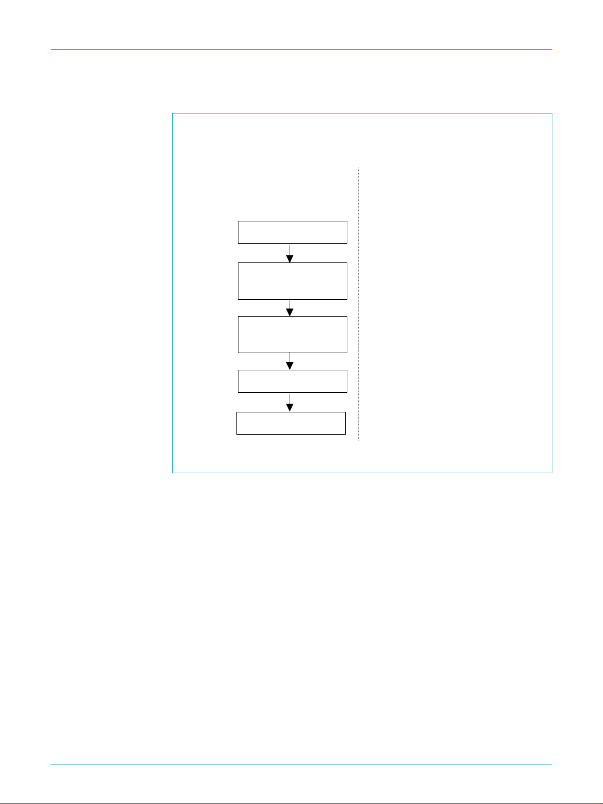
I2C Master
I2C Start Condition
Device Address
(r/w = 0)
4 bytes subaddress
(= PI bus address)
4 bytes data
I2C Stop Condition
I2C Slave (PNX2000)
Figure 2: Single Write
UM10105_1 © Koninklijke Philips Electronics N.V. 2003. All rights reserved.
Rev. 1.0 — 28 November 2003 2-3
Page 22
Philips Semiconductors
PNX2000
Control Interface
Single Read
I2C Master
I2C Start Condition
Device Address
(r/w = 0)
4 bytes subaddress
(= PI bus address)
I2C Repeat - Start
Condition
Device Address
(r/w = 1)
I2C Slave (PNX2000)
4 bytes data
I2C Stop Condition
Figure 3: Single Read
UM10105_1 © Koninklijke Philips Electronics N.V. 2003. All rights reserved.
Rev. 1.0 — 28 November 2003 2-4
Page 23

Philips Semiconductors
PNX2000
Control Interface
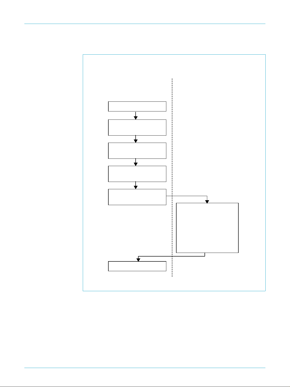
Burst Write
I2C Master
I2C Start Condition
Device Address
(r/w = 0)
4 bytes subaddress
(= PI bus address)
4 bytes data
4 bytes data
…(as many 4 - byte
words as desired)
I2C Slave (PNX2000)
PNX2000 will
internally increment
the PI - Bus address
for each data word
I2C Stop Condition
Figure 4: Burst Write
UM10105_1 © Koninklijke Philips Electronics N.V. 2003. All rights reserved.
Rev. 1.0 — 28 November 2003 2-5
Page 24
Philips Semiconductors
Burst Read
PNX2000
Control Interface
I2C Master
I2C Start Condition
Device Address
(r/w = 0)
4 bytes subaddress
(= PI bus address)
Repeat - Start
Condition
Device Address
(r/w = 1)
I2C Slave (PNX2000)
4 bytes data
4 bytes data
…(as
many 4 - byte data
words as desired).
The PNX2000 will
internally increment
the PI - Bus address
for each data word.
I2C Stop Condition
Figure 5: Burst Read
2.2.4 I2C Interface Block
The I2C interface module contains no software-accessible status or configuration
registers.
If the internal PI-Bus locks up, the I
holding the SCL signal low. The only way to break the lockup is to reset the entire
PNX2000 device. In order to avoid this condition, the BCU timeout register should be
configured by software early in the PNX2000 initialization process.
UM10105_1 © Koninklijke Philips Electronics N.V. 2003. All rights reserved.
Rev. 1.0 — 28 November 2003 2-6
2
C interface will lock the external I2C bus by
Page 25

Philips Semiconductors
The PNX2000 I2C module will not respond to a ‘general call’ on the I2C-bus, i.e. when
a slave address of 0000000 is sent by a master. In case of any illegal address,
transmission of the data that follows is not acknowledged, and the transmission is
aborted.
The I
400 kbits/s in accordance with the I
2.3 BCU Module
2.3.1 BCU Features
The BCU module performs the following functions:
PNX2000
Control Interface
2
C-bus slave devices are capable of operating at a maximum speed of
• Address space mapping and slave selection
• Bus error notification and logging
• Bus timeout monitoring, with software programmable timeout threshold
2
C fast-mode specification.
• Interrupt generation on bus error and timeout
2.3.2 Registers
The BCU contains eight software accessible registers which are listed in
the following table. Note that the base address of the BCU is 0x07fe8000.
The “reset” values given in the tables in the following subsections correspond to the
state of a variable after PI-Bus reset.
Table 1: BCU Register Map
Register Name
BCU_INT_STATUS 0x00 BCU interrupt status
BCU_INT_SET 0x04 BCU interrupt status set
BCU_INT_CLEAR 0x08 BCU interrupt status clear
BCU_FAULT_STATUS 0x0C BCU bus fault status
BCU_FAULT_ADDRESS 0x10 BCU bus fault address
BCU_INT_ENABLE 0x14 BCU interrupt enable
BCU_TOUT 0x18 BCU time-out control
BCU_SNOOP 0x1C BCU memory coherency control
Offset from BCU
Slave address
Description
UM10105_1 © Koninklijke Philips Electronics N.V. 2003. All rights reserved.
Rev. 1.0 — 28 November 2003 2-7
Page 26

Philips Semiconductors
2.3.2.1 BCU Interrupt Status Register (BCU_INT_STATUS)
This register contains the BCU interrupt status variables. It is read-only. The register
also controls the bus fault logging process.
Table 2: BCU_INT_STATUS register
Bits Variable Reset R/W
31:2 RSD - -
1 BCU_TO 0 R
0 BCU_BE 0 R
RSD Reserved bits, will produce zero on a read action and ignored on write
BCU_TO Time-out error:
PNX2000
Control Interface
action
0: no time-out error has occurred. Fault logging enabled if BCU_BE=0
and BCU_TO=0.
1: time-out error has occurred. Fault logging stopped. Registers
BCU_FAULT_STATUS and BCU_FAULT_ADDRESS contain valid
information. Depending on the state of the BCU_INT_EN flag in the
BCU_INT_ENABLE register, an interrupt request may be generated.
BCU_BE Bus error:
0: no bus error has occurred. Fault logging enabled if BCU_TO=0 and
BCU_BE=0.
1: bus error has occurred. Fault logging stopped. Registers
BCU_FAULT_STATUS and BCU_FAULT_ADDRESS contain valid
information. Depending on the state of the BCU_INT_EN flag in the
BCU_INT_ENABLE register, an interrupt request may be generated.
2.3.2.2 BCU Interrupt Enable Register (BCU_INT_ENABLE)
This register contains a variable to enable/disable BCU interrupt request generation.
It is read/writable. Note that this register does not have two enable bits (i.e.
corresponding to the two status bits in the BCU_INT_STATUS, BCU_INT_SET, and
BCU_INT_CLEAR registers). One enable bit controls the generation of both bus error
and timeout interrupts.
Table 3: BCU_INT_ENABLE register
Bits Variable Reset R/W
31: 1 RSD - R
0 BCU_INT_EN 0 R/W
RSD Reserved bits, produce zero on read action and ignored on
write.
BCU_INT_EN BCU Interrupt Enable
0: disable BCU interrupt request.
UM10105_1 © Koninklijke Philips Electronics N.V. 2003. All rights reserved.
Rev. 1.0 — 28 November 2003 2-8
Page 27

Philips Semiconductors
2.3.2.3 BCU Interrupt Status Set Command (BCU_INT_SET)
A write action to this address location allows to set variables in the
BCU_INT_STATUS register. A read action returns 0. The BCU_INT_SET command
is provided for diagnostic purposes only.
Table 4: BCU_INT_SET command
Bits Variable Reset R/W
31:2 RSD - R
1 BCU_TO_SET - W
0 BCU_BE_SET - W
RSD Reserved bits, produce zero on read action and ignored on a write.
BCU_TO_SET Time-out interrupt set:
PNX2000
Control Interface
1: enable BCU interrupt request. An interrupt request is
generated when the BCU_TO and/or BCU_BE flags in the
BCU_INT_STATUS register are set.
0: no effect
1: set BCU_TO variables
BCU_BE_SET Bus error interrupt set:
0: no effect
1: set BCU_BE variables
2.3.2.4 BCU Interrupt Status Clear Command (BCU_INT_CLEAR)
A write action to this address location allows to clear variables in the
BCU_INT_STATUS register. A read action returns 0.
Table 5: BCU_INT_CLEAR command
Bits Variable Reset R/W
31:2 RSD - R
1 BCU_TO_CLEAR - W
0 BCU_BE_CLEAR - W
RSD Reserved bits, produce zero on read action and ignored on a write.
BCU_TO_CLEAR Time-out interrupt clear:
0: no effect
1: set BCU_TO variables
BCU_BE_CLEAR Bus error interrupt clear:
0: no effect
1: clear BCU_BE variables
UM10105_1 © Koninklijke Philips Electronics N.V. 2003. All rights reserved.
Rev. 1.0 — 28 November 2003 2-9
Page 28

Philips Semiconductors
2.3.2.5 BCU Bus Fault Status Register (BCU_FAULT_STATUS)
This register captures status information on the PI-Bus operation that incurred a bus
error or time-out. The register content is valid only when the BCU_TO and/or
BCU_BE flags in BCU_INT_STATUS are set. The register is read-only. Note that the
PNX2000 design has only one bus master - the I
Table 6: BCU_FAULT_STATUS Register
Bits Variable Reset R/W
31:8 RSD - -
7 BCU_MASTER* X R
6 BCU_LOCK X R
5 BCU_READ X R
4:0 BCU_OPC X R
[6-1] * BCU_MASTER is not relevant for PNX2000
[6-2] X undefined
RSD (Reserved bits) will produce zero on a read action and will be ignored on a write
action.
2
C interface.
PNX2000
Control Interface
BCU_LOCK LOCK status of failed bus operation:
0: LOCK = 0
1: LOCK = 1
BCU_READ Data direction of failed bus operation:
0: write operation
1: read operation
BCU_OPC Opcode of failed bus operation:
refer to PI-Bus specification [2] for opcode definition.
2.3.2.6 BCU Bus Fault Address Register (BCU_FAULT_ADDR)
This register captures the address in a PI-Bus operation that incurred a bus error or
time-out. The register content is valid only when the BCU_TO and/or BCU_BE flags
in BCU_INT_STATUS are set. The register is read-only.
Table 7: BCU_FAULT_ADDR Register
Bits Var iable Reset R/W
31:2 BCU_ADDR X R
1:0 RSD 0 R
[7-1] X undefined
BCU_ADDR failed bus operation address
RSD reserved bits, produce zero on a read action ignored on a write
UM10105_1 © Koninklijke Philips Electronics N.V. 2003. All rights reserved.
Rev. 1.0 — 28 November 2003 2-10
Page 29

Philips Semiconductors
2.3.2.7 BCU Time-Out Register (BCU_TOUT)
This register defines the PI-Bus time-out threshold. It is read/writable. Although this
register has a default value of 0, it should be written with the value 0x800 soon after
reset, to prevent potential PI-Bus and I
Table 8: BCU_TOUT Register
Bits Variable Reset R/W
31: 0 BCU_TO_THRESHOLD 0 R/W
BCU_TO_THRESHOLDTime-out threshold:
2.3.2.8 BCU Memory Coherency Register (BCU_SNOOP)
PNX2000
Control Interface
2
C bus lockups.
0: never time-out
st
1: time-out after 1
4294967295: time-out after 4294967295th data cycle in bus
operation
data cycle in bus operation
This register enables/disables the start of the memory coherency protocol. This
register should be left at the default value, as the PNX2000 device does not support
cache-coherent memory access.
Table 9: BCU_SNOOP Register
Bits Variable Reset R/W
31:3 RSD X R
2 BCU_SNOOP_MASTERS 0 R/W
1 BCU_SNOOP_WRITE 0 R/W
0 BCU_SNOOP_READ 0 R/W
[9-1] X undefined
RSD Reserved bits, produce zero on a read action ignored on a
write
BCU_SNOOP_MASTERS Bit not relevant for PNX2000. To be left at default value.
BCU_SNOOP_WRITE Bit not relevant for PNX2000. To be left at default value.
BCU_SNOOP_READ Bit not relevant for PNX2000. To be left at default value.
UM10105_1 © Koninklijke Philips Electronics N.V. 2003. All rights reserved.
Rev. 1.0 — 28 November 2003 2-11
Page 30

Philips Semiconductors
2.4 Memory Map
The PNX2000 memory map is given in the following table. Note that the address
ranges allocated to each block are not fully occupied by addressable register
locations.
Table 10: Memory Map
PI Bus Address Block
0x07F0.0000
0x07F3.FFFF
0x07F8.0000
0x07FB.FFFF
0x07FE.8000
0x07FE.8FFF
0x07FF.5000
0x07FF.5FFF
0x07FF.7000
0x07FF.7FFF
0x07FF.8000
0x07FF.8FFF
0x07FF.9000
0x07FF.9FFF
0x07FF.A000
0x07FF.AFFF
AUDIO_DSP
DEMDEC DSP
BCU
DCU
GPR(GTU)
2
I
D
VIDDEC
ITU656
PNX2000
Control Interface
UM10105_1 © Koninklijke Philips Electronics N.V. 2003. All rights reserved.
Rev. 1.0 — 28 November 2003 2-12
Page 31

3.1 Introduction
Chapter 3: I2D
PNX2000 User Manual
Rev. 1.0 — 28 November 2003
This section provides an overview of the I2D link and how it may be applied. It gives
the user a guide to use the datalink and its functions. The purpose of the link is
transmitting data in three streams from the PNX3000 to the PNX2000. The use of
serial data connections results in a considerable reduction in pin count and the
number of connection wires that are needed between both IC’s.
The communication between one datalink transmitter and one datalink receiver
consists of two signals, a data signal and a strobe signal. The strobe signal contains
the data, bit-sync and word-sync information. For optimal EMC performance both
data and strobe are low voltage differential signals. The voltage swing on the wires is
about 300mV.
In the PNX3000 the video and audio data to be transmitted is multiplexed in an output
register of 42 bits. The content of that 42-bit register is serial transmitted on one of the
three datalinks. In the PNX2000 the serial data is demultiplexed into parallel streams.
With a software selection in the PNX3000 you can choose which data you want to set
in the output register for the datalink and in the PNX2000 you have to make a
selection which data from the datalink you want to use. The data on the datalink is
divided in several groups of signals (video, audio and strobe_signals). It is important
that the transmitter and receiver are in the same transmitting mode.
Page 32

Philips Semiconductors
d
U
Data Link
r
r
A
PNX2000
I2D
CVBS/Y-prim
CVBS/Y-prim
ICLP
2nd SIF/ 2
CVBS_sec
ICLP
Yyu
ICL
L1/AMint
R1/AMext
MIC/L2/PipM
n
SIF
Clk
54M
Clk
54MH
Clk
27/54M
Clk
27/54M
Clk
6.75MH
54MHz
Data Link
54MHz
Data Link 2
54MHz
DataLink
DataLi
DataLink
DataLink
PNX2000
I2D
Receive
4
D
I2D
Receiver
I2D
Receive
4
4
Clock
Domain
Separators
D
D
Xtal Clk
54MHz
Conf.
Registers
D
4
D
4
D
4
DTL
Controller
Demux_mode
VAL
Demux and
Formatter
PI toDTL
dapter
10
10
10
10
1+
1+
1+
1+
10
1+
1+
CVBS/
Yyuv/C
UV
CVBSs
L1
L2
R2
L2
SIF
HV
HV sec
MIC/R2
Figure 1: Overview - I2D Transmitter/Receiver
3.2 Functional Capabilities of the Links
The I2D link has the following characteristics.
• The datalink runs at 297MHz / 594 Mbs.
• The driver rise/fall time is around 200 pS.
• The datalink uses differential signals.
The receiver has an internal termination resistor of 100Ω differential connected.
• The differential threshold is 50 mV.
• The signalling voltages are between 200 – 500 mV.
• The datalink traces, both pairs should be of equally length and are internally
terminated with 100Ω (The PCB-lines also characteristic).
UM10105_1 © Koninklijke Philips Electronics N.V. 2003. All rights reserved.
Rev. 1.0 — 28 November 2003 3-2
Page 33

Philips Semiconductors
R
R
2
yuv
1
yuv
3
3.3 Transmitter
In the PNX3000 the data coming from the A/D converters (digital video and audio) is
multiplexed and put in data words. Each data word on the data links consists of 44
bits (4 video samples of 10 bits each, 2 audio samples of 2 bits and 2 word-sync bits).
The word clock is 13.5MHz. The data rate on each of the three data links is 44 bits/
cycle*13.5*106 Cycle/s=594Mbit/s. Figure 2
these can be sent to the digital video processor by the datalink. Mode 0 is the 1fh
mode and mode 1 is the 2fh mode (for datalink 1 and 2). Both modes can transferred
up to three video channels plus one sound IF signal and two L+R audio signals over
the data links simultaneously. For detailed transmission information see Table 2
PNX2000
I2D
• The max length of the datalink tracks is 20 cm (equal length), normal advice is 5
cm maximal.
• The maximal capacitance on the line is around 15 pF.
shows which signals are digitized and
.
ModApplication
0 T CVBS/Yp Cpri L
1 YUV 2 L R U V L R SI X X
n
Yyuv
Figure 2: Overview - Datalink Modes, Transmitter Side PNX3000
Y
Data
Video Audio
Yyuv
Yyuv
n+
Y
n+
Yyu U, L
n+
Data Data
Test Video VideoAudio
SI X X
R1
L1
UM10105_1 © Koninklijke Philips Electronics N.V. 2003. All rights reserved.
Rev. 1.0 — 28 November 2003 3-3
Page 34

Philips Semiconductors
d
PNX2000
I2D
CVBS/Y-prim
CVBS/Y-prim
C
ICLP
2nd SIF/ 2
CVBS_sec
ICLP
Yyuv
ICLP
ICLP
U
V
ICLP
L1/AMint
R1/AMext
MIC/L2/PipM
MIC/R2
n
SIF EXT
A
A
A
A
A
A
D
Clk
54MHz
10
D
Clk
54MHz
D
Clk
27/54MHz
D
Clk
27/54MHz
D
Clk
6.75MHz
D
10
Data
Link 1
DataLink
DataLink
54MHz 297MHz
Data
Link 3
10
54MHz 297MHz
10
2
2
Data
Link 2
54MHz 297MHz
DataLink
DataLink
Clk
6.75MHz
Figure 3: Simplified Transmitter Side PNX3000
3.4 Receiver
The I2D datalink is intended for the communication between the PNX3000 and the
PNX2000.
2
The I
D receiver module consists of three datalink receivers, and three Data Strobe
receivers. The data receiver regenerates the serial data bit-streams, and converts
them to parallel words of 42 bits (picture 4x10 bits and 2 bits of audio). When the data
is ready for output a valid Word Sync pulse is generated in the I
The Word Sync pulses are used by the clock domain separator to take over the 42
bits wide data from the I
UM10105_1 © Koninklijke Philips Electronics N.V. 2003. All rights reserved.
Rev. 1.0 — 28 November 2003 3-4
2
D receivers to the PNX2000 clock domain.
2
D receiver module.
Page 35

Philips Semiconductors
The clock domain separator module converts the data from the transmitter clock
(13.5 or 27 MHz) domain (PNX3000) to the PNX2000 clock (13.5 / 54 MHz) domain.
There is a clock domain separator necessary because the signals in the PNX3000
are processed via different paths and then multiplexed on a serial data line with a
Data Strobe (and Word Sync). This leads to a static but unknown phase difference
between the PNX2000 and PNX3000 clock. In addition, the duration of the serial data
differs according the link length and group of data on the link and the different
processing in the PNX3000. That is why a clock domain separator is necessary.
The data from the clock domain separator module is passed to the de-multiplexer
module. This module formats the data into several audio and video streams (parallel
data) together with accompanying VALid pulses derived from the clock domain
separator (ready for takeover) to the Viddec and Demdec modules.
PNX2000
I2D
When the expected Word Sync pulse is not detected in the I
2
D receiver, the clock
domain separator still generates a DV pulse. The previous data is still on the parallel
output lines of the I
2
D receiver. When the Word Sync pulse is not detected, the
counter counts the missing DataValids. This internal counting continues until it
reaches the DV_MISS_MAX value (Table 8
reached, an interrupt DVx_MISS_STAT is generated, ref to Ta bl e 11
). When the limit of DV_MISS_MAX is
for more details,
and a synchronization action must follow. When the limit is reached the internal
counter is frozen.
When the max value of DV_MISS_MAX is not reached and a Word Sync pulse
arrives in the receiver window, the counter DV_MISS_MAX is reset.
When there is a situation in which the expected Word Sync pulse is detected in the
2
I
D receiver, but not within the data valid window (receiver window) of the Clock
domain Separator, the pulse is Out Of Window (OOW). The clock domain separator
generates a Data Valid (DV) pulse on the time that the clock domain separator
expects to receive a Word Sync pulse from the receiver. The data can still be valid if
the pulse comes to early, but if the pulse comes to late, the previous data can be on
the output when the clock domain separator takes the data over. When the Word
Sync pulse is out of his window detected, it generates an Out Of Window (OOW)
pulse (referring to I2D _REC_SYNC_LOST). This Out Of Window pulse increments
the counter (it counts the OOW pulses), the counter value itself cannot be read. This
counting continues till it reaches the OOW_MAX value (register I2D
_REC_SYNC_LOST). When the limit of OOW_MAX is reached, an interrupt
SYNCx_LOST_STAT is generated, ref to I2D _INT_STATUS for more details, and a
synchronization action must follow. When the max value of OOW_MAX is not
reached and a Word Sync pulse arrives in the receiver window, the counter
OOW_MAX is reset.
At the end of the receiver is a de-multiplexer, the de-multiplexer reformats the data
into several audio and video streams (parallel data) to the Viddec and Demdec.The
functional block diagram of the receiver is shown in Figure 4
UM10105_1 © Koninklijke Philips Electronics N.V. 2003. All rights reserved.
Rev. 1.0 — 28 November 2003 3-5
.
Page 36

Philips Semiconductors
eceiver
eceive
A
s
PNX2000
I2D
PI bu
DataLink
DataLink
DataLink
DataLink
Conf.
DV
42
DV
42
DV
Register s
42
Demux and
Formatter
Cloc k
Domai n
Separator s
I2D
I2D
R
I2D
R
DV
42
DV
42
DV
42
r
Xtal Clk
54MHz
DTL
Control
I2D REC INT
Demux_mode
VAL
PI toDTL
dapter
10+1
10+1
10+1
10+1
1+1
1+1
1+1
1+1
10+1
1+1
1+1
CVBS/Yyc
Yyuv/Cyc
UV
CVBSsub
L1
L2
R2
L2
SIF
HV
HV_s ec
Figure 4: Simplified Receiver Side PNX2000
3.4.1 Transmitter / Receiver Transmission Modes.
The data from the PNX3000 can be sent in two modes (0, 1) to the receiver in the
PNX2000. Ta ble 1
transmitter in the PNX3000 has to be set by the external I
microprocessor in the PNX2000 transmits the mode settings and other multiplexer
settings by the I
configured in the same mode by the PI bus in the PNX2000. In Ta bl e 1
the dataflow and possible modes on each link. The software for the receiver runs in
the MIPS processor in the PNX2000. The software takes care of the boot sequences,
interrupts and the use of the data on the datalink.
When the transmitter is in mode 0 (all three transmitters are in mode 0), the receiver
has the possibility to extract data in mode 0a en 0b (for all three links together). This
is possible due to the group of 42 bits send together, see Figure 1
UM10105_1 © Koninklijke Philips Electronics N.V. 2003. All rights reserved.
describes the data that can be extracted from the datalink. The
2
C communication link. The
2
C bus to the PNX3000. The receiver in the PNX2000 has to be
is described
and Table 2.
Rev. 1.0 — 28 November 2003 3-6
Page 37

Philips Semiconductors
When Viddec uses Y and C from mode 0 datalink 1, it can’t use YUV from datalink 2
(no sync available, they use the same bus in the demultiplexer output). If the Viddec
use YUV from datalink 2 (input from RGB in PNX3000) it use the CVBS datalink 1 for
sync.
Table 1: Content of Data Links
Datalink 1 Bits
mode setting mode reg
value
mode 0a 0x0 R1 L1 C
mode 0b 0x1 R1 L1 - CVBS or Y
mode 1 0x2 R1 L1 Yyuv
Datalink 2 Bits
mode setting mode reg
value 41 40 39:30 29:20 19:10 9:0
mode 0a 0x0 R2 L2 - - - -
mode 0b 0x1 R2 L2 V
mode 1 0x2 R2 L2 V
41 40 39:30 29:20 19:10 9:0
n+2
n+1
n+1
n+1
n
C
- CVBS or Y
n+1
Yyuv
n
U
n
V
n+1
n
n+2
n+3
CVBS or Y
Yyuv
Yyuv
n+2
U
PNX2000
CVBS or Y
Yyuv
Yyuv
n
U
n
n
n
n
I2D
Datalink 3 Bits
mode setting mode reg
value
41 40 39:30 29:20 19:10 9:0
mode 0a 0x0 HV
mode 0b 0x1 HV
mode 1 0x2 HV
A CVBS or Y signal may be connected to the inputs of the PNX3000. The type of
signal on Datalink 1, in Mode 0 (a or b) is not known, but the preferred is shown bold
underlined.
If from datalink 1 (mode 0b) the CVBS is used, via fast insertion the Viddec can use
the YUV (1fH-mode) signals from datalink2 if the signal contains a sync signal.
Figure 5
output of the multiplexer.
HV SIF
sec
HV SIF
sec
HV SIF
sec
n+1
n+1
n+1
CVBSsec
CVBSsec
CVBSsec
n+1
n+1
n+1
SIF
SIF
SIF
n
n
n
CVBSsec
CVBSsec
CVBSsec
, Figure 6 and Figure 7 show the use modes (video) in the receiver at the
n
n
n
UM10105_1 © Koninklijke Philips Electronics N.V. 2003. All rights reserved.
Rev. 1.0 — 28 November 2003 3-7
Page 38

Philips Semiconductors
PNX2000
I2D
Data Link 1
Data Link 2
Data Link 3
Demux
Figure 5: Mode 0a Transmission
Data Link 1
Data Link 2
Data Link 3
Demux
Figure 6: Mode 0b Transmission (Default)
Y/C or CVBS
CVBS
YUV
VIDDEC
VIDDEC
Data Link 1
Data Link 2
Data Link 3
Demux
Y
UV
VIDDEC
Figure 7: Mode 1 Transmission (2fh on Main Channel, on sub is 1fh)
The control software has to set the right settings in the MPIF and AVIP.
3.4.2 Data Rate and Timing Output Signals
The output rate of the data from the datalink receiver is shown in Table 2 .
The HV_PRIM and HV_SEC are for the horizontal and vertical sync for the primary
and secondary channel (timing pulses in IF part). These are clamping signals, which
are coming from the VIDDEC. The frequency of the signals is dependent of the select-
UM10105_1 © Koninklijke Philips Electronics N.V. 2003. All rights reserved.
Rev. 1.0 — 28 November 2003 3-8
Page 39

Philips Semiconductors
ed mode. These signals are not needed for I2D link.
Table 2: Data Rate Output Signals
Pin Name Sample Rate (Msamples/s)
CVBS_YYC_OUT 27 -
YYUV_CYC_OUT 27 54
UV_OUT 27 54
CVBS_SEC_OUT 27 -
LEFT1_OUT 6.75
RIGHT1_OUT 6.75
LEFT2_OUT 6.75
RIGHT2_OUT 6.75
HV_OUT 54
HV_SEC_OUT 54
SIF_OUT 27
PNX2000
I2D
1FH 2FH
All data is generated on the negative edge of the 54 MHz clock.
3.5 Configuration Registers.
The I2D configuration registers are used to control the I2D receiver module. For
description of the de-multiplexer outputs see following figure.
Figure 8: Read Write and Control Flow
UM10105_1 © Koninklijke Philips Electronics N.V. 2003. All rights reserved.
Rev. 1.0 — 28 November 2003 3-9
Page 40

Philips Semiconductors
PNX2000
I2D
The I2D configuration register block contains the control registers which are used to
configure the I
2
D receiver block, address decoder and two state machines. One to
synchronise the write request and the register write enable, and the other one to
synchronise the read request and read enable.
3.5.1 I2D Register Map
This section provides information on the I2D configuration. Each of the registers
within the receiver block is described separately below. The base address for the I
is set to 0x07FF8000 (32 bits), the last 3 digits (12 bits) are for the I
register.
Table 3: I2D Register Summary
Name Access Type Width Address Reset Value
I2D _RX_CTRL Read/Write 32 0x000 0x1
I2D _RX_STATUS Read 32 0x004 0x1
I2D _MOD_ID Read 32 0xFFC 0x01410000
I2D _INT_SET Write 32 0xFEC 0x00000000
I2D _INT_CLEAR Write 32 0xFE8 0x00000000
I2D _INT_ENABLE Read/Write 32 0xFE4 0x00000000
I2D _INT_STATUS Read 32 0xFE0 0x0000002a
I2D _REC_DEMUX_MODE Read/Write 32 0x018 0x0001fff9
I2D _PRBS_CTRL Read/Write 32 0x024 0x00000000
I2D _PRBS_STAT Read/Write 32 0x020 0x00000078
I2D _REC_SYNC_LOST Read/Write 32 0x01C 0x000003e8
2
D control
2
D
3.5.1.1 I2D_RX_CTRL
Table 4: I2D_RX_CTRL
Bits Name Access Type Reset Value Description
31..01 RSD_31 To 1 Reserved 0x0 Reserved
0 RX_APPL_PD Read/Write 0x1 Power down for analogue receiver in application mode.
'0' : The analogue receiver is active (normal mode)
'1' : The analogue receiver is in power down mode (For
PNX2000 sleep/coma modes)
2
This is the bit to wake up or set the I
D receiver in power down mode.
UM10105_1 © Koninklijke Philips Electronics N.V. 2003. All rights reserved.
Rev. 1.0 — 28 November 2003 3-10
Page 41

Philips Semiconductors
PNX2000
3.5.1.2 I2D_RX_STATUS
Table 5: I2D_RX_STATUS
Bits Name Access Type Reset Value Description
31..01 RSD_31 To 1 Reserved 0x0 Reserved
0 PD_STAT_RX Read 0x1 Power down status of analogue datalink receiver.
'0' : The receiver is active (normal mode)
'1' : The receiver is in power down mode
This is a status bit to verify if the datalink receiver is really activated or if it was still in
power down mode. When the I2D_RX_CTRL bit 0 differs from the I2D_RX_STATUS
bit 0, there is a hardware problem, probably due to an internal test mode.
3.5.1.3 I2D_REC_DEMUX_MODE
Table 6: I2D _REC_DEMUX_MODE
Bits Name Access Type Reset Value Description
31..18 RSD_31 To 18 Reserved 0x0 Reserved
17 SOFT_RESET Write Only 0x0 Soft_reset of the clock domain separator
16 DATA_VALID_MASK Read/Write 0x1 Mask the overall data valid flag (to enable data output to the
cores). '1' Enable '0' Hide
11..3 VALID_MASK Read/Write 0x1ff Mask data valid of several type of data busses. Each bit: '0' to
hide. Bit no: [11]= SIF ; [10] =Right 2; [9]= Left 2;; [8]= Right 1;
[7] =Left 1 ;[6] =CVBS sec; [5]= U ;[4] =Y ; [3] =CVBS.
2:0 DEMUX_MODE Read/Write 0x1 Select the I2D content format to output mode '000' mode 0a
'001' mode 0b '010' mode 1
I2D
• Soft_reset is not latched, it resets (unlock) the clock domain separator. Read first
the I2D _REC_DEMUX reg. Then OR with bit 17 and then write back the register.
• Data_valid_mask is connected to clock domain separator to control (enable 1 /
disable 0) data_valid signal. Default (hard reset) value is enabling (1), with this bit
you enable or disable all data Valid signals. It is recommended that this bit is not
used.
• Valid_mask (bit 3 - 11) is connected to the demultiplexer block to control (enable
1/disable 0) the demultiplexer valid output signals for the desired buses. Default
(hard reset) is 0x1FF hex (enable all). When the Valid signal comes from the
Clock domain separator, the output data from the multiplexer is ready and has to
be read. When the Valid signal is a (0), the data is invalid. Every parallel signal
coming from the demultiplexer can be accompanied with the appropriate data
valid pulse derived from the Clock domain separator. This pulse can be enabled
by setting a value ‘1’ to its respective bit shown in the table below to the item
VALID_MASK of the register REC_DEMUX_MODE. To prevent crosstalk, it is
recommended to enable the data valid signals for the ones in use.
Table 7: Demultiplexer Output with Mask Selection
Data bus Bit Position VALI D_MASK Data link
SIF 12 (0x100)
R2 11 (0x80)
L2 10 (0x40)
H
H
H
3
2
2
UM10105_1 © Koninklijke Philips Electronics N.V. 2003. All rights reserved.
Rev. 1.0 — 28 November 2003 3-11
Page 42

Philips Semiconductors
PNX2000
I2D
Table 7: Demultiplexer Output with Mask Selection
Data bus Bit Position VALI D_MASK Data link
R1 9 (0x20)
L1 8 (0x10)
CVBS
sec
UV 6 (0x04)
Yyuv / Cyc 5 (0x02)
CVBS
/ Yyc 4 (0x01)
pri
7 (0x08)
…Continued
H
H
H
H
H
H
1
1
3
2
1
1
Demux_Mode (bit 0 – 2) is connected to the demultiplexer block to select the data
mode on the demultiplexer output. Default value is 0x01 bin. (Mode 0B, seeFigure 6
3.5.1.4 I2D _REC_SYNC_LOST
Sync lost timer before generating an interrupt.
Table 8: I2D_REC_SYNC_LOST
Bits Name Access Type Reset Value Description
31..16 DV_MISS_MAX Read/Write 0x3e8 Number of consecutive valid pulses missing before
generating an dv error interrupt '0' disables detection
and resets the counter
15..0 OOW_MAX Read/Write 0x3e8 Number of consecutive valid pulses out of the catching
window before generating an 'out of sync' (sync lost)
interrupt' 0' disables detection and resets the counter
)
DV_MISS_MAX[31..16] (16 bits) is connected to the clock domain separator to set
the maximum value of consecutive missing data valid pulses. The default (Hard
reset) value is 0x3E8 (1000 dec). When the maximum value is reached an interrupt
'DVx_MISS_STAT’ is generated for the appropriate link (see register INT_STATUS).
OOW_MAX[15:0] (16 bits) is connected to the clock domain separator to set the
maximum value of consecutive out of window data valid pulses. The default (Hard
reset) value is 0x3E8 (1000 dec). When the maximum value is reached an interrupt
'SYNCx_LOST_STAT’ is generated for the appropriate link, (see register
INT_STATUS).
Remark: To ensure proper counting during lowering this value, first write a value of 0
into the DV_MISS_MAX or OOW_MAX value. Otherwise, the counter marker may be
shifted over the max_count, which will result in a 16 bit overcount (afterwards it will
continue at 0).
If an interrupt is to be cleared, the following procedure must be followed:
1. Write a 0x0 into OOW_MAX and DV_MISS_MAX register to disable detection
and reset the counter.
2. Clear the appropriate link in the <XREF>12D_INT_CLEAR register (for all write
3F).
3. Write the requested value to the OOW_MAX and DV_MISS_MAX register, then
write a 0 in the 12D_INT_CLEAR register.
UM10105_1 © Koninklijke Philips Electronics N.V. 2003. All rights reserved.
Rev. 1.0 — 28 November 2003 3-12
Page 43

Philips Semiconductors
PNX2000
3.5.1.5 I2D _PRBS_STAT
Pseudo Random Bit Sequence checksum status. In this PRBS mode there is a biterror check on the content of the datalink, not on the datalink itself. The PRBS mode
can be used for bit-error rate analysis. The functions of OOW and DV_MISS are still
working.
Table 9: I2D_PRBS_STAT
Bits Name Access Type Reset Value Description
31..7 RSD_31 To 7 Read Only 0x0 Reserved
6 DV_UNDET Read Only 0x1 Global data valid undetected
'1' DV undetected yet
'0' DV has been detected
5 DV3_UNDET Read Only 0x1 Data valid of datalink 3 undetected
'1' DV undetected yet
'0' DV has been detected
4 DV2_UNDET Read Only 0x1 Data valid of datalink 2 undetected
'1' DV undetected yet
'0' DV has been detected
3 DV1_UNDET Read Only 0x1 Data valid of datalink 1 undetected
'1' DV undetected yet
'0' DV has been detected
2 DLINK3_ERROR Read Only 0x0 Error on datalink 3
1 DLINK2_ERROR Read Only 0x0 Error on datalink 2
0 DLINK1_ERROR Read Only 0x0 Error on datalink 1
I2D
This mode is only useful for debug/test mode and for testing of the datalinks. This
mode is not necessary for application. It can be used to check the datalink channels
on data transfer.
3.5.1.6 I2D _PRBS_CTRL
Pseudo Random Bit Sequence checksum settings.
Table 10: I2D_PRBS_CTRL
Bits Name Access Type Reset Value Description
31..8 RSD_31 To 8 Reserved 0x0 Reserved
7 PRBS_ENABLE Read/Write 0x0 (1) Enable check on Pseudo Random Bit
Sequence, (0) is normal mode and no check on
PRBS.
6 DV_UNDET_SET Write Only 0x0 Set data valid detection status to undetected for
global dv
5 DV3_UNDET_SET Write Only 0x0 Set data valid detection status to undetected for
datalink 3
4 DV2_UNDET_SET Write Only 0x0 Set data valid detection status to undetected for
datalink 2
3 DV1_UNDET_SET Write Only 0x0 Set data valid detection status to undetected for
datalink 1
UM10105_1 © Koninklijke Philips Electronics N.V. 2003. All rights reserved.
Rev. 1.0 — 28 November 2003 3-13
Page 44

Philips Semiconductors
Table 10: I2D_PRBS_CTRL
Bits Name Access Type Reset Value Description
2 DL3_ERR_RST Write Only 0x0 Clear error status bit of datalink 3
1 DL2_ERR_RST Write Only 0x0 Clear error status bit of datalink 2
0 DL1_ERR_RST Write Only 0x0 Clear error status bit of datalink 1
[10-1] The DLx_ERR_RST registers don’t always work well. To clear the DLINKx_ERROR status in the I2D_PRBS_STATUS register,
the PRBS_ENABLE (bit 7) should be toggled off and on again.
PNX2000
[10-1]
[10-1]
[10-1]
This mode is only useful for debug mode, and for application not necessary. The
testing of datalinks is not necessary in normal mode, but can be usefull to check the
data transfer over the datalink.
3.5.1.7 I2D _INT_STATUS
The status of (possible) DVP interrupt requests.
Table 11: I2D _INT_STATUS
Bits Name Access Type Reset Value Description
31..6 RSD_31 To 6 Reserved 0x0 Reserved
5 DV3_MISS_STAT Read Only 0x0 Data valids are missing for datalink 3. The max value
dv_miss_max has been reached.
4 SYNC3_LOST_STAT Read Only 0x0 Data valid out of sync indication for datalink 3. The max
value oow_max for out of window dv pulses has been
reached.
3 DV2_MISS_STAT Read Only 0x0 Data valids are missing for datalink 2. The max value
dv_miss_max has been reached.
2 SYNC2_LOST_STAT Read Only 0x0 Data valid out of sync indication for datalink2. The max
value oow_max for out of window dv pulses has been
reached.
1 DV1_MISS_STAT Read Only 0x0 Data valids are missing for datalink1. The max value
dv_miss_max has been reached.
0 SYNC1_LOST_STAT Read Only 0x0 Data valid out of sync indication for datalink1. The max
value oow_max for out of window dv pulses has been
reached.
I2D
In this register you can read the status of the link if there are missing data valid errors,
and if there has been loss of sync on one of the datalinks.
3.5.1.8 I2D _INT_ENABLE
Enable the DVP (Digital Video Platform) interrupt for request to the system IRQ
controller.
Table 12: I2D _INT_ENABLE
Bits Name Access Type Reset Value Description
31..6 RSD_31 To 6 Reserved 0x0 Reserved
5 DV3_MISS_ENA Read/Write 0x0 Enable interrupt for missing data valid of datalink 3
4 SYNC3_LOST_ENA Read/Write 0x0 Enable interrupt for lost of sync of datalink 3
3 DV2_MISS_ENA Read/Write 0x0 Enable interrupt for missing data valid of datalink 2
UM10105_1 © Koninklijke Philips Electronics N.V. 2003. All rights reserved.
Rev. 1.0 — 28 November 2003 3-14
Page 45

Philips Semiconductors
Table 12: I2D _INT_ENABLE
Bits Name Access Type Reset Value Description
2 SYNC2_LOST_ENA Read/Write 0x0 Enable interrupt for lost of sync of datalink 2
1 DV1_MISS_ENA Read/Write 0x0 Enable interrupt for missing data valid of datalink 1
0 SYNC1_LOST_ENA Read/Write 0x0 Enable interrupt for lost of sync of datalink 1
PNX2000
With this register you can enable or disable interrupts.
3.5.1.9 I2D _INT_CLEAR
Clear DVP interrupts. The I2D _INT_CLEAR is not a register, but a trigger
mechanism.
Table 13: I2D_INT_CLEAR
Bits Name Access Type Reset Value Description
31..6 RSD_31 To 6 Reserved 0x0 Reserved
5 DV3_MISS_CLR Write Only 0x0 Clear indication for missing data valid of datalink 3
4 SYNC3_LOST_CLR Write Only 0x0 Clear indication for lost of sync of datalink 3
3 DV2_MISS_CLR Write Only 0x0 Clear indication for missing data valid of datalink 2
2 SYNC2_LOST_CLR Write Only 0x0 Clear indication for lost of sync of datalink 2
1 DV1_MISS_CLR Write Only 0x0 Clear indication for missing data valid of datalink 1
0 SYNC1_LOST_CLR Write Only 0x0 Clear indication for lost of sync of datalink 1
I2D
To clear the interrupts, write a 0 into OOW_MAX and DV_MISS_STAT registers. Then
clear the INT_CLEAR register (write 3F, for reset all) and write the OOW_MAX and
DV_MISS_STAT value (recommended is 0x50).
3.5.1.10 I2D _INT_SET
Set a DVP interrupt.
Table 14: I2D _INT_SET
Bits Name Access Type Reset Value Description
31..6 RSD_31 To 6 Reserved 0x0 Reserved
5 DV3_MISS_SET Write Only 0x0 Simulate data valids are missing for datalink3. The max
value DV_MISS_MAX has been reached.
4 SYNC3_LOST_SET Write Only 0x0 Simulate data valid out of sync indication for datalink3. The
max value OOW_MAX for out of window DV pulses has
been reached.
3 DV2_MISS_SET Write Only 0x0 Simulate data valids are missing for datalink2. The max
value DV_MISS_MAX has been reached.
2 SYNC2_LOST_SET Write Only 0x0 Simulate data valid out of sync indication for datalink2. The
max value OOW_MAX for out of window DV pulses has
been reached.
1 DV1_MISS_SET Write Only 0x0 Simulate data valids are missing for datalink1. The max
value DV_MISS_MAX has been reached.
0 SYNC1_LOST_SET Write Only 0x0 Simulate data valid out of sync indication for datalink1. The
max value OOW_MAX for out of window DV pulses has
been reached.
UM10105_1 © Koninklijke Philips Electronics N.V. 2003. All rights reserved.
Rev. 1.0 — 28 November 2003 3-15
Page 46

Philips Semiconductors
This register allows the software to simulate a missing data valid, or loss of sync on
one or more links.
3.5.1.11 I2D _MOD_ID
Table 15: I2D _MOD_ID Block information
Bits Name Access Type Reset Value Description
31..16 MODULE_ID Read Only 0x141 Module identifier
15..12 MAJOR_REV Read Only 0x0 Major Revision. Any revision that may break SW compatibility.
11..8 MINOR_REV Read Only 0x0 Minor Revision. Any revision that still keep SW compatibility.
7..0 APERTURE Read Only 0x0 Aperture Size.
In this register you can read the hardware version. With the software version
identified you have a better overview of the hardware/software capabilities. Also, the
software can have better control over the modules if hardware version is known.
PNX2000
3.6 Interrupt Procedure
I2D
When the I2D core detects an interrupt condition, i.e. a situation that requires
software interaction, it sets the corresponding Internal Interrupt Status bit in the
Interrupt Status register. Then the I
enabled by inspecting the corresponding bit in the Interrupt Enable register. If this bit
is ‘1’, a system interrupt request will be generated.
The software should remove the cause of the interrupt condition by taking the
appropriate action. As soon as the cause is removed, the Internal Interrupt Status bit
in the Interrupt Status register must be cleared by writing a ‘1’ to the corresponding bit
of the Interrupt Clear register.
For debugging purposes the software can also generate ‘fake’ interrupt conditions by
writing a ‘1’ into bit i of the Interrupt Set register. The result is that the Interrupt Status
bit i will go high.
3.6.1 Interrupt Behaviour
The I2D interrupt architecture contains 4 registers: status, enable, set and clear.
Activation of an interrupt request starts as soon as the interrupt condition becomes
true. The interrupt condition can be read from the status register, its name indicates
the interrupt generated. Every interrupt condition (set interrupt or write action) can set
bits in the status register. The status register indicates one or more pending interrupt
conditions.
To disable interrupts:
2
D checks whether this interrupt condition is
• via register INT_ENABLE to enable/disable interrupts on a line
• via setting OOW_MAX and DV_MISS_MAX to 0x0.
To c l e a r interr u p t s :
• write 0x0 in DV_MISS_MAX and OOW_MAX register
• clear the interrupts via register INT_CLEAR (write 0x3F to it)
UM10105_1 © Koninklijke Philips Electronics N.V. 2003. All rights reserved.
Rev. 1.0 — 28 November 2003 3-16
Page 47

Philips Semiconductors
3.6.2 Software Action with Registers
When an interrupt occurs, the reaction of the system is set maker dependent. It is
recommended to execute the soft-reset procedure. A software loop should check
whether the fault situation won’t occur again (polling or via interrupts). There are
several operating situations that can occur:
1. Start up
2. Normal operation
3. Soft_reset
4. Change of source selection
5. Sync lost on a datalink
6. Missing of data valid pulses
7. Test mode: pseudo random mode, set interrupt status bit for lost data and/or sync
PNX2000
I2D
• set default value 0x50 in DV_MISS_MAX and OOW_MAX register
3.6.2.1 Start Up
During startup, registers will have a default value after releasing the reset to the I2D
receiver registers.
The bit 0 in I2D_RX_CTRL has to activate the receiver. A 0 has to be written to it, by
startup the bit is: 1 (power down), needed to power down the HF datalink receiver in
sleep and coma modes. Enabling is needed for normal operations.
During startup the clock domain separator has to lock on the Data Valid signals. After
power up all the I2D interrupt sources are disabled. The clock domain separator block
is waiting for Data Valids (validity the data of the corresponding datalink) coming from
the three analog datalinks. If there are Data Valids on at least two data_links, which
are in the same clock period, the clock domain separator is locked on these pulse
rates.
Procedure at start up:
• Activate the receiver in reg: I2D _RX_CTRL, bit 0 (RX_APPL_PD) write 0.
• Disable the DV_MISS_MAX and OOW_MAX counter, by writing a 0, (disable int)
• Give a Soft_Reset, in I2D _REC_DEMUX_MODE write bit 17.
• Write 3F to the INT_CLEAR,
• Enable the DV_MISS_MAX and OOW_MAX counter and write defaut 0x50, the
minimum value is 2.
After this soft-reset the clock domain receiver locks again and the Data and Strobe
Signals should be stable. The receiver should now enter Normal operation, if not refer
to conditions 5 and 6 below.
UM10105_1 © Koninklijke Philips Electronics N.V. 2003. All rights reserved.
Rev. 1.0 — 28 November 2003 3-17
Page 48

Philips Semiconductors
3.6.2.2 Normal Operation
During normal operation PNX2000 sends an operating status signal to the PNX3000
receiver (1 per second). When the receiver is in lock, the clock domain separator
continues to check that the Data Valid pulses are coming in the right window from the
datalinks. If the clock domain separator does not get Data Valid pulses within the
desired window, the number of MISsing Data Valid, or Out Of Window pulses, from
the corresponding link is incremented. If the number missing Data valid pulses to the
de-multiplexer is larger than OOW_MAX, or DV_MISS_MAX, the interrupt status is
set and an interrupt can be generated. When this happens, operating condition 5 or 6
occur.
Remark: If the clock domain separator does not get Data Valid signal within the
desired window, the data can still be valid.
3.6.2.3 Soft_reset
When a fault condition appears the clock domain separator gets out of lock (no data
pulses are detected within the window), when the limit of OOW_MAX or
DV_MISS_MAX is reached. However, the software resets the Rec_Demux_mode
register 07FF8018 and bit 17 from this register resets the clock domain separator and
the receiver can again lock on the data-stream.
PNX2000
I2D
Such a fault condition appears during start-up, for this reason the receiver is powered
down during switch on.
A temperature change, or start-up transient can cause fast phase shift of the datalink
and the clock domain receiver does not receive DV pulses within the catching or
locking window.
3.6.2.4 Change of Source Selection
When there is a request to change the video source, the AVIP sends a command via
the I2C bus telling the MPIF that it has to change the source. When the MPIF
changes the source, the Data Valids generated in the receiver are still right, but the
content from a packet is not right (due to the asynchronous switch over). The
MIPS_software itself has to find out where the MPIF has changed over. The change
over is in one packet.
3.6.2.5 Sync lost on a datalink (Out Of Sync)
When the counter OOW_MAX counts too many word sync out of the locked window
(meaning a number of such words, counted by a counter, exceeds the value set via
OOW_MAX item), the output data is not stable anymore. A sync_lost indicator is
raised, meaning SYNC3_LOST_STATSYNC2_LOST_STATSYNC2_LOST_STAT is
set to '1'. Change in value of a sync_lost indicator from '0' to '1' should be a trigger for
software to perform a soft_reset action to calibrate the clock domain again in order to
guarantee a good picture and sound quality.
The following steps can be executed in this situation:
1. Set a soft_reset item from the I2D_REC_DEMUX_MODE register to '1' in order to
calibrate the clock domain.
UM10105_1 © Koninklijke Philips Electronics N.V. 2003. All rights reserved.
Rev. 1.0 — 28 November 2003 3-18
Page 49

Philips Semiconductors
2. Write '0' into OOW_MAX item and afterwards write back again the chosen value
3. Clear the interrupts by writing 0x3F into I2D_INT_CLEAR register.
This calibration loop is needed to ensure a proper picture on the output. Otherwise
there can appear speckles on the screen and sound can be disturbed. Software can
decide whether they regular poll the status register or enable the interrupt.
In normal circumstances this interrupt should not appear. But when it does, software
should act as described in this section to ensure good picture and sound quality.
3.6.2.6 Missing data_valid pulses
When the clock domain separator doesn't receive word sync pulses, the
DV_MISS_MAX counter for a respective link is incremented. However each
consecutive time a word sync (or data valid) is received, the DV_MISS_MAX counter
of the appropriated datalink is reset. When the counter reaches the programmed
value, defined in DV_MISS_MAX register, the corresponding bit of the INT_STATUS
register (DV3_MISS_STAT or DV2_MISS_STAT or DV1_MISS_STAT) is set to 1 and
the datalink receiver generates an interrupt flag.
PNX2000
I2D
(recommended is 0x50). This action is necessary to clear the internal Out Of
Window counters.
If there is an indicator of data valid missing raised, meaning DV3_MISS_STAT
DV2_MISS_STAT DV1_MISS_STAT is set to '1', it is likely that the output data is
invalid. Change in value of a data valid missing indicator from '0' to '1' should be a
trigger for software to perform a recovery in order to guarantee a good picture and
sound quality.
The following steps can be executed in this situation:
1. Check the status of the datalink receivers. The RX_APPL_PD of the
I2D_RX_CTRL register should be set 0 and the PD_STAT_RX (bit 0) of
I2D_RX_STATUS should be equal. If this status bit is 1, there is an internal
hardware problem and should be stored in the Error register.
2. Set a soft_reset item from the I2D_REC_DEMUX_MODE register to '1' in order to
calibrate the clock domain again.
3. Write '0' into DV_MISS_MAX and afterwards write back again the chosen value
(recommended is 0x50). This action is necessary to clear the internal DV_MISS
counter.
4. Clear the interrupts by writing 0x3F into I2D_INT_CLEAR.
5. Put PPRS_ENABLE to '1' to start measurements on the I2D Receiver.
6. If the DV_UNDET bit remains high in 100ms, the I2D can not lock anymore to the
input. If the DVx_UNDET bits remain high in 100 ms, the corresponding data
valid did not arrive at all. In this situation, there is an external (hardware) problem
and should be logged into the Error register.
7. If the interrupt returns within 1 second, there is an external (hardware) problem of
bad reception and should be logged into the Error register.
UM10105_1 © Koninklijke Philips Electronics N.V. 2003. All rights reserved.
Rev. 1.0 — 28 November 2003 3-19
Page 50

Philips Semiconductors
Software can decide whether they regular poll the status register or enable the
interrupt. In normal circumstances this interrupt will never appear. But when it does
(due to a hardware defect or external factors), software should act as proposed in this
section. It is up to the custumer whether this software loop is implemented and if the
errors are logged in the Error register.
It is advised to blank the picture output when this condition appears, since the data is
corrupted. Most likely Viddec won't be able to lock and sound is disturbed. Check
whether the MPIF is booted up and functioning properly.
3.6.2.7 Test mode
It is not possible to do a boundary scan of the datalink transmitters in the MPIF and it
is not possible to do a boundary scan of the inputs of the AVIP receiver. So it is very
difficult to test the ICs on those points. Therefore it is possible to bring the MPIF in
pseudo-random mode (from version MPIF N1D). In this mode the manufacturer can
evaluate the transmitter-receiver link on various data profiles and analyze the link
behavior.
This test mode can be used to evaluate the data transfer from MPIF to AVIP.
PNX2000
I2D
The procedure is described below.
1. Blank the picture on the screen and switch off the sound output, to avoid noise on
the screen and noise out of the speakers.
2. Set the MPIF in pseudo-random mode via the PRND bit from the MPIF
Datalink_mode register. See user manual MPIF.
3. Write a '1' to Soft_reset from the I2D_REC_DEMUX_MODE register to calibrate
the clock domain again.
4. Set the OOW_MAX and DV_MISS_MAX counter in register: REC_SYNC_LOST
to 0x0. (Disables counter and interrupts generation) and write back again the
chosen value (recommended is 0x50).
5. Clear the I2D_INT_CLEAR register by writing 0x3F.
6. Activate the Pseudo-Random Bit Sequence check. Write 1 to PRBS_ENABLE
(bit 8) of the I2D_PRBS_CTRL register.
7. When the PRBS mode is activated, the circuit checks the data coming from the
MPIF. Afterwards poll the Pseudo Random Bit Sequence status (PRBS_STAT)
register regular. The value of this register should be 0x0.
– When the DVx_UNDET did not become '0', the datalink did not receive any
datavalid from the HF datalink receivers.
– When the DLINKx_ERROR is '1', it means the pseudo-random data was not
right on the line the corresponding error bit. This bit stays high until it is cleared
by toggling PRBS_ENABLE.
– When Interrupt DVx_MISS_STAT is high, the data valid does not appear
regular.
– When Interrupt SYNCx_LOST_STAT is high, the datalink is not calibrated well.
A soft_reset could be executed to calibrate again.
The working of PRBS registers is independent of the OOW and DV_MISS counters.
The data speed on the line is very high, so you know immediately if the line is good.
UM10105_1 © Koninklijke Philips Electronics N.V. 2003. All rights reserved.
Rev. 1.0 — 28 November 2003 3-20
Page 51

Philips Semiconductors
If no errors are observed during execution of the test, software can again switch off
the PRBS mode of MPIF and the I2D receiver and release the system (i.e. enable
sound and picture output).
If there are errors it means that:
PNX2000
I2D
• The transmitter in the MPIF is not functioning,
• The receiver in the AVIP is not functioning,
• The wire connection is not good (with one open wire it was found that the
transmission was still good. (The wire connection can be checked with the DCF
status bit of MPIF).
• There are outside disturbances (e.g. EMC, power stability).
UM10105_1 © Koninklijke Philips Electronics N.V. 2003. All rights reserved.
Rev. 1.0 — 28 November 2003 3-21
Page 52

4.1 Overview
Chapter 4: Video Processing (Viddec)
PNX2000 User Manual
Rev. 1.0 — 28 November 2003
VIDDEC has the following features:
• AGC on all inputs to ensure optimum use of the bit range
• CVBS and Y/C input
• Multi-standard Color decoder including PAL M and PAL N
• 2D Comb Filter
• YPrPb / RGB processing, both 1Fh and 2Fh
• Sync on CVBS, Y or external (external 2Fh only)
• Fast blanking for RGB on SCART (1Fh only)
The input can handle CVBS, Y/C and YUV signals.
Remark: The system can handle also RGB signals because the PNX3000 converts
RGB signals to YUV. The Y from YUV and C from Y/C share the same channel. In
practice, Y/C and YUV are not present at the same time, so this is no limitation.
The signals from the I
block. All incoming data streams are 10 bits wide and have the same sample
frequency. U and V, which are sampled at half the sample frequency of CVBS, C and
Y, are combined in one data stream.
The U and V stream is demultiplexed in separate U,V streams for further processing.
In the sample rate converter the data streams are transferred from the free running
sample clock to a line locked clock domain. At the same time the data sample size is
increased to 13 bit.
2
D receiver block are fed to the input of a data synchronizer
Page 53

Philips Semiconductors
PNX2000
Video Processing
Figure 1: Block Diagram VIDeo DECoder
The 13 bit wide data streams enter the AGC block. This block takes care to fit the
incoming signals optimally in the available 9 bit space for further processing in the
chain. Level deviations at the PNX3000 inputs from +3 dB to – 3dB are corrected. In
this way no excessive headroom needs to be reserved which improves the signal to
noise in the chain. The sync signal has a separate AGC block. The input for the Sync
AGC can be taken from the CVBS/Y channel or from the Y channel from YUV.
The CVBS and Y/C data are fed to a multi-standard color decoder. This decoder can
handle all world standards of PAL, SECAM and NTSC including Latin America. All
necessary filtering and traps are included. The input of the color demodulator can be
switched between the CVBS signal and the C signal to enable Y/C processing. The
decoder also incorporates a 2D combfilter for PAL (4 lines) and NTSC (2 lines) for
improved luminance and chrominance separation.
The YUV at the output of the color decoder connect to an YUV switch. At the other
input of this switch the YUV signals from the YUV input are connected. The switch
can be controlled by an external voltage (Fast Blanking on insertion pin) or forced by
software. A formatter combines the U and V stream again to one data stream with the
same sample frequency as the Y stream The sync output from the AGC goes to the
synchronization block. This block generates the Horizontal and Vertical pulses for
further processing (HVsync), as well as timing information for the PNX3000 for
correct black level clamping (HVinfo).
The YUV path and the synchronization can handle both 1Fh signals as 2Fh signals.
For 2 Fh signals, the sampling frequency for YUV is doubled and also the
synchronization uses a special 2 Fh part for sync processing.
UM10105_1 © Koninklijke Philips Electronics N.V. 2003. All rights reserved.
Rev. 1.0 — 28 November 2003 4-2
Page 54

Philips Semiconductors
The sync can be derived from the Y signals or from external H and V pulses. Also
ATSC YUV signals (tri level sync and Fh = 33.75 kHz) can be handled in 2 Fh mode.
To process 2Fh signals, the VIDDEC must be set in 2Fh mode by doubling one of its
clock frequencies coming from another block in PNX2000.
4.2 Data input, Sample Rate Converter and timing
Figure 2 shows typical input and sample rate conversion.
PNX2000
Video Processing
Figure 2: Input and Sample Rate Conversion
4.2.1 Short Description
The input can handle CVBS, Y/C and YUV. To distinguish the Y from Y/C and from
YUV the first is called Yyc and the second Yyuv. Cyc and Yyuv share the same data
path. The selection which signal is routed to the input is made by the I
block.
UM10105_1 © Koninklijke Philips Electronics N.V. 2003. All rights reserved.
Rev. 1.0 — 28 November 2003 4-3
2
D receiver
Page 55

Philips Semiconductors
Figure 3 shows the data streams from I2D to VIDDEC for different modes.
PNX2000
Video Processing
Figure 3: Selection Input Data Streams for VIDDEC in I2D
For 1 Fh, all input data streams are 10 bit, sampled with 27 MHz derived from a free
running system clock. For 2 Fh, the Y and multiplexed UV data stream have a sample
rate of 54 MHz.
In the first block the data is converted from unsigned to signed and the UV data
stream is demultiplexed in separate U and V streams. The data streams are then fed
to a sample rate converter. The samples are converted from the free running system
clock domain to a (gated) line locked clock domain. (see PNX8550 for more
information)
The number of bits per sample is increased to 13 bits at the output to enable optimal
processing in the next AGC block.
UM10105_1 © Koninklijke Philips Electronics N.V. 2003. All rights reserved.
Rev. 1.0 — 28 November 2003 4-4
Page 56

Philips Semiconductors
4.3 AGC
PNX2000
Video Processing
Figure 4: AGC Block Diagram
4.3.1 Short Description
The up converted 13 bit wide signals, coming from the sample rate converter, are
passed through an AGC stage to utilise the full 9 bits resolution of the color decoder.
The CVBS/Y, U and V signal path have their own AGC circuit, the Cyc and Yyuv
share the AGC circuit because these signals are not available at the same time.
Selection between Cyc and Yyuv is done in the I
At the input of the Sync AGC circuit, it is possible to select between the CVBS/Yyc
signal or the Yyuv signal for sync processing.
The AGC stage consists of a general programmable gain stage and a control circuit.
The gain stage is identical for all input signals. It features:
• Programmable black level for the input stage
• Programmable black level for the output stage
• Programmable gain range
For gain stages, which only carry one type of signal (CVBS/Yyc, U, V, Sync), the
settings are fixed.
2
D receiver with the bits mode1..0.
UM10105_1 © Koninklijke Philips Electronics N.V. 2003. All rights reserved.
Rev. 1.0 — 28 November 2003 4-5
Page 57

Philips Semiconductors
For gain stages carrying different signals (Cyc or Yyuv) the settings must be adapted
for the selected signal. There are 3 control circuits, one for CVBS/Yyc, one for Cyc or
Yyuv, one for Sync signal, each adapted for the specific signal properties. The control
options are:
PNX2000
Video Processing
• Control on Sync amplitude
• Setting target sync amplitude
• Control on Peak White (Only CVBS/Yyc, Cyc or Yyuv)
• Setting target Peak White amplitude (Only CVBS/Yyc, Cyc or Yyuv)
• Minimal gain
• Maximal gain
• Fixed gain (No AGC)
• Hold momentary gain
In addition, the CVBS/Yyc control circuit can also use the (external) Peak White
Limiter of the Color Decoder to adapt the gain. The U and V gain stages are slaved to
the Cyc/Yyuv gain stage and the Cyc/Yyuv control circuit. At the output the streams
are 9 bits wide. The signals are routed to the Color decoder (CVBS/Yyc and Cyc), to
the YUV switch (Yyuv, U, V) and to the Sync circuit (CVBS/Yyc or Yyuv).
4.3.2 AGC Gain Stages
Figure 5: AGC Gain Stages
UM10105_1 © Koninklijke Philips Electronics N.V. 2003. All rights reserved.
Rev. 1.0 — 28 November 2003 4-6
Page 58

Philips Semiconductors
The 10 bits wide data, coming from the I2D receiver, are up converted to 13 bits by
the sample rate converter before entering the AGC gain stage. This implies that the
incoming data is multiplied with a factor of 8.
The gain stage is made universal for all channels, and to adapt the stage to the
specific input/output requirements, the black level at the input
(ctrl_blanking_offset_in), the gain (ctrl_divider) and the black level at the output
(ctrl_blanking_offset_out) are programmable.
After the gain stage, the data width is brought back to 9 bits wide to fit the data width
of the processing by the color decoder. Beside the data width, also the black level and
signal format (signed or unsigned) is adapted for the next stage. Below, a survey is
given from the input data versus output data of the AGC stage. In the picture, the
maximum data value, the minimum data value and the blanking level is indicated.
PNX2000
Video Processing
Figure 6: Input Format vs. Output Format of AGC
As indicated, different signals need different conversion. Especially the AGC gain
stage in the Cyc / Yyuv path needs attention, because it has to be configured
differently depending on the selected signal path.
Table 1: Bit Description - AGC Gain Stages - Address 0X7FF9xxx
add
xxx Bits Name Function R/D R/W
040 2 dmsd_sync_sel_y Selects sync input 2 Sync from CVBS/Yyc
path (1Fh) 3 Sync from Yyuv path (1Fh or
2Fh)
084 31..29 agc_cvbs_yyc_divider Sets amplification range of the AGC block 3 R/W
24..16 agc_cvbs_yyc_blanking_offset_out Sets output blanking level 138 R/W
UM10105_1 © Koninklijke Philips Electronics N.V. 2003. All rights reserved.
Rev. 1.0 — 28 November 2003 4-7
0/x R/W
Page 59

Philips Semiconductors
PNX2000
Video Processing
Table 1: Bit Description - AGC Gain Stages - Address 0X7FF9xxx
add
xxx Bits Name Function R/D R/W
7..0 agc_cvbs_yyc_blanking_offset_in Sets input blanking level 80 R/W
088 31..29 agc_y_cyc_divider Sets amplification range of the AGCblock 4/3 R/W
24..16 agc_y_cyc_blanking_offset_out Sets output blanking level 138/1C0 R/W
7..0 agc_y_cyc_blanking_offset_in Sets input blanking level 80/0 R/W
08C 31..29 agc_crcb_divider Sets amplification range of the AGC block 3 R/W
24..16 agc_crcb_blanking_offset_out Sets output blanking level C0 R/W
7..0 agc_crcb_blanking_offset_in Sets input blanking level 0 R/W
080 31..29 agc_sync_divider Sets amplification range of the AGC block 6 R/W
24..16 agc_sync_blanking_offset_out Sets output blanking level 138 R/W
7..0 agc_sync_blanking_offset_in Sets input blanking level 80 R/W
…Continued
Remark: In all Bit Description tables the R/D column indicates Reset/Default. If
default value is not given it is the same as the reset.
dmsd_sync_sel_y
The sync for the synchronization block can be taken from the CVBS/Yyc path or the
Cyc/Yyuv path. The Cyc/Yyuv path can also be used for 2Fh signals with sync on
Yyuv.
Remark: For 1Fh RGB signals, the sync is often taken from the (accompanying)
CVBS signal.
agc_xxx_divider
The divider sets the maximum gain of the stage. The first part of the stage is a preamplifier, whose gain can range between a minimum of 0 and a maximum of 1023.
The gain can be controlled by the AGC loop or programmed for a fixed gain
(see Section 4.3.3
Figure 7: AGC Universal Programmable Gain Stage
)
The programmable part of the gain stage consists of 3 parallel branches (dividers),
which can be selected individually or in combination. The amplification of the 3
branches at maximum pre-amplifier gain (1023) is 0.2500, 0.1250 and 0.0625
respectively and are controlled by agc_xxx_divider bits 2..0 in the same order.
UM10105_1 © Koninklijke Philips Electronics N.V. 2003. All rights reserved.
Rev. 1.0 — 28 November 2003 4-8
Page 60

Philips Semiconductors
So the gain range from the 13 bits input to the 9 bits output of the summation block
can be set between:
Remark: At least one branch has to be enabled.
This gain is finally multiplied by the fixed gain of the following block. This fixed gain is
not equal for all AGC gain stages.
In formula:
gain = pre-amp gain (dec) * ((div(2)*0.25 + div(1)*0.125 + div(0)*0.0625) / 1023) *
fixed gain
Programming
For the AGC divider stages of CVBS/Yyc, CrCb (Uyuv/VYuv) and Sync, the reset
value is the required value. No need to program these values.
PNX2000
Video Processing
• Minimal gain, agc_xxx_divider = 0 0 1 [binary] is 0.0625
• Maximum gain, agc_xxx_divider = 1 1 1 [binary] is 0.4375
Only for the Cyc/Yyuv stage, programming is needed, depending on the selected
signal path:
• Yyuv signal (YPrPb or RGB): agc_y_cyc_divider = 3 hex (bit 011)
• Cyc signal: agc_y_cyc_divider = 4 hex (bit 100)
agc_xxx_blanking_offset_in
Looking at the input format, we have two standard blanking levels at the input, 0 (0
hex) and –2176 (1780 hex two's complement). The selection between these two
levels is made by the most significant bit of AGC_xxx_blanking_offset_in (bit 7):
• agc_xxx_blanking_offset_in (7) = 0 selects offset 0 (0 hex)
• agc_xxx_blanking_offset_in (7) = 1 selects offset -2176 (1780 hex, two's
complement)
The bits agc_xxx_blanking_offset_in (6..0) control the offset in two's complement
mode. Resolution per step is 4 hex on the 13 bit wide input data, i.e. one step
increases the 13 bit data by 4 hex. Calculating back the resolution to the 10 bits data
at the output of the I
is ½ LSB on the 10 bits data, which is fine enough for this purpose.
The offset control is mainly to correct problems of black level offsets in previous
stages like the AD conversion. For PNX2000, no black level offset correction is
needed. So only the most significant bit 7 is used to select between the two standard
blanking levels at the input.
2
D receiver (or input of the sample rate converter), the resolution
Programming
For the AGC stages of CVBS/Yyc, CrCb (Uyuv/VYuv) and Sync, the reset value is the
required value. No need to program these values. Only for the Cyc/Yyuv stage,
programming is needed, depending on the selected signal path:
UM10105_1 © Koninklijke Philips Electronics N.V. 2003. All rights reserved.
Rev. 1.0 — 28 November 2003 4-9
Page 61

Philips Semiconductors
agc_xxx_blanking_offset_out
At the output, we have more difference in required format. The signals fed to the color
decoder are formatted in two's complement, while signals following the YUV path, are
unsigned. The blanking level has now to be programmed correctly for each signal
path. The offset value is 9 bits wide and has a resolution of 1 LSB/step related to the
9 bits wide output. The range is (in two's complement) –256 to 255. To have enough
range for the offset programming, an offset of 64 dec (40 hex) is added. This shifts
the range to – 192 to 319 The formula to calculate the needed offset value is:
(decimal): agc_xxx_blanking_level_offset_out(dec) = required blanking level(dec)
– 64
(hex): agc_xxx_blanking_level_offset_out(hex) = required blanking level(hex) – 40
For the required blanking level the value is given in Figure 7 Input format vs. output
format of AGC. Except for agc_y_cyc_blanking_offset_out, the needed value
equals the reset value:
PNX2000
Video Processing
• Yyuv signal: agc_y_cyc_blanking_offset_in = 80 hex (bit 7 = 1)
• Cyc signal: agc_y_cyc_blanking_offset_in = 0 hex (bit 7 = 0)
agc_sync_blanking_offset_out = 138 (hex)
agc_cvbs_yyc_blanking_offset_out = 138 (hex)
agc_crcb_blanking_offset_out = C0 (hex)
agc_y_cyc_blanking_offset_out
The gain stage for the (combined) Cyc / Yyuv path contains an extra formatter stage
which contains a fixed gain and transforms the output levels of Yyuv to the levels,
suited to feed to the YUV switch. For the calculation of the
agc_y_cyc_blanking_level_offset_out for use with Yyuv we have to use the levels
before the formatter.
So the blanking level for Yyuv out is –136 dec (178 hex two's complement).
Using the formula the value for Yyuv becomes –200 dec (138 hex).
The blanking level for Cyc is 256.
The value for use with Cyc becomes 192 dec (C0 hex)
The range of the agc_xxx_blanking_offset_out is larger than needed for the
application in PNX2000.
It is possible to program the offset so high that the value of the output is higher than
the output range of 9 bits. In that case, the value is not clipped but folds over.
Because these high settings are not practical for PNX2000 other than for testing, this
is no limitation. In practice, the described values should be used, which have no
problems.
UM10105_1 © Koninklijke Philips Electronics N.V. 2003. All rights reserved.
Rev. 1.0 — 28 November 2003 4-10
Page 62

Philips Semiconductors
Programming
For the AGC stages of CVBS/Yyc, CrCb (Uyuv/VYuv) and Sync, the reset value is the
required value. No need to program these values.
Only for the Cyc/Yyuv stage, programming is needed, depending on the selected
signal path:
4.3.3 AGC Control Circuit
PNX2000
Video Processing
• Yyuv signal: agc_y_cyc_blanking_offset_out = -200 dec (138 hex, two's
complement)
• Cyc signal: agc_y_cyc_blanking_offset_out = 256 dec (C0 hex)
Figure 8: AGC Control Circuit CVBS/Yyc and Yyuv/Cyc
4.3.3.1 AGC Control Circuit for CVBS / Yyc path
The control circuit for the CVBS / Yyc path has a very flexible set-up. It is designed to
work in an automatic mode. In this case, the sync amplitude is used to determine the
needed gain factor for amplification of the total signal to the nominal level. To cope
with signals having compressed sync, a peak white limiter will take care that no
clipping occurs. In the CVBS / Yyc control circuit it is possible to use the AGC internal
peak white limiter or the "external" peak white limiter of the color decoder.
UM10105_1 © Koninklijke Philips Electronics N.V. 2003. All rights reserved.
Rev. 1.0 — 28 November 2003 4-11
Page 63

Philips Semiconductors
PNX2000
Video Processing
To improve the behavior for non-standard conditions, the maximum and minimum
gain can be programmed to prevent excessive adaptation. It is also possible to set a
fixed gain for test purposes. Also the gain of an active loop can be frozen for
measuring or testing.
The time constant of the AGC loop can be programmed differently for the situation
when there is horizontal lock (usually a fast time constant required) or when there is
no horizontal lock (usually slower time constant to prevent pumping). For this
purpose, the horizontal lock of the sync circuit is used. For monitoring, an interrupt
can be programmed to signal when the programmed gain limits are exceeded.
Table 2: Bit Description - AGC Gain Control - Address 0X7FF9xxx
add
Bits Name Function R/D R/W
xxx
094 9.0 agc_cvbs_yc_ctrl_gainvalue_pi Gain value when forcegain_pi = 1 1CD R/W
10 agc_cvbs_yc_ctrlagc_cvbs_yc_ct
rl_forcegain_pi
11 agc_cvbs_yc_ctrl_holdgain_pi 0 Normal AGC loop operation1 Freezes the momentary
18..16 agc_cvbs_yc_ctrl_tau_catch_pi AGC loop time constant when there is no H-lock
22..20 agc_cvbs_yc_ctrl_tau_inlock_pi AGC loop time constant when there is H-lock000 Fast
23 agc_cvbs_yc_ctrl_pw_ext_pi Enables the "external" (= outside AGC block) peak white
24 agc_cvbs_yc_ctrl_pw_int_pi Enables the internal peak white limiter of the AGC block to
25 agc_cvbs_yc_ctrl_sync_int_pi Enables the sync AGC loop to apply the same
26 agc_cvbs_yc_ctrl_copy_prot_pi Corrects the nominal sync amplitude to 80% for
0A0 19..10 agc_cvbs_yyc_ctrl_low_gain_lim
_pi
0A4 19..10 agc_cvbs_yyc_ctrl_up_gain_lim_piSets maximum possible gain for the AGC loop 39A R/W
0 Gain controlled by AGC loop. 1 Fixed gain, determined
by gainvalue_pi
gain of the loop
000 Fast AGC time constant. 111 Slow AGC time constant
AGC time constant111 Slow AGC time constant
limiter of the multi-standard color decoder to influence the
AGC loop. 0 External pk wh lim not enabled
1 External pk wh lim enabled
influence the AGC loop0 Internal pk wh lim not enabled1
Internal pk wh lim enabled
multiplication to the CVBS / YYC amplifier as needed to
bring the sync amplitude to nominal level 0 Control by
sync AGC loop not enabled1 Control by sync AGC loop
enabled
macrovision signals. Must be used when macrovision is
detected (dmsd_copro = 1) 0 Normal operation1 Use
reduced sync amplitude(80%)
Sets lowest possible gain for the AGC loop 142 R/W
0R/W
0R/W
1R/W
6R/W
1R/W
1R/W
1R/W
0R/W
08 19..10 agc_cvbs_yc_monitor_hwgain Readout of the momentary gain value of the AGC loop R
FE0 13 ics_agc_cvbs_yc_gain_limit Interrupt flag set to 1 when upper or lower gain limit is
exceeded. See Section 4.4.8
UM10105_1 © Koninklijke Philips Electronics N.V. 2003. All rights reserved.
Rev. 1.0 — 28 November 2003 4-12
for details
R
Page 64

Philips Semiconductors
agc_cvbs_yc_ctrl_gainvalue_pi / _forcegain_pi
When agc_cvbs_yc_ctrl_forcegain_pi is set to 1, the gain of the AGC stage is
determined by the setting of register agc_cvbs_yc_ctrl_gainvalue_pi. The 10 bits of
this register determine the amplification of the pre-amplifier, discussed in AGC Gain
Stages bit agc_xxx_divider.
The gain can be set from 0 to 1023.
The total amplification from input (13 bits) to output (9 bits) can be calculated using
the formula, given in the description of the agc_xxx_divider bit:
gain = pre-amp gain (dec) * ((div(2)*0.25 + div(1)*0.125 + div(0)*0.0625) / 1023) *
fixed gain. Taking into account that the fixed gain in the sync path is 1:
gain = gainvalue_pi (dec) * ((div(2)*0.25 + div(1)*0.125 + div(0)*0.0625) / 1023) * 1.
div(w) = agc_xxx_divider(w) where w is the bit number.
PNX2000
Video Processing
To scale the gain from 13 bit to the 10 bits wide output of the I
2
D receiver (or input of
the sample rate converter), the found gain value has to be multiplied by 8.
agc_cvbs_yc_ctrl_holdgain_pi
Implemented for test purposes to freeze the momentary gain.
agc_cvbs_yc_ctrl_ctrl_tau_catch_pi / _inlock_pi
While catching signals, the AGC time constant has to be fast to adapt quickly to
varying signals conditions during e.g. search tuning. When in lock, the AGC time
constant can better be chosen larger to prevent unstable behavior like pumping on
video content. Because it is possible to program different time constants when not in
lock (fast) and when in lock (less fast) the loop values do not need reprogramming
depending on the signal condition. The values for these registers after a reset should
perform ok.
agc_cvbs_yc_ctrl_pw_int_pi / _pw_ext_pi / sync_int_pi
These bits enable the different control loops.
When the amplitude of the total signal is attenuated proportionally but the relative
amplitude ratios are kept correct, the sync amplitude is the most ideal signal part to
determine the needed amplification to bring the signal back to nominal level.
Only for compressed sync, the amplification would become too large. The external
peak white limiter (present in the color decoder / Y processing part) can be used to
reduce the gain below peak white level. Also the internal peak white limiter in the
AGC can perform this task, but this peak white limiter clips immediately signals when
coming above peak white level, while the external peak white limiter is more
sophisticated in behaviour. It is advised to enable all three control circuits for the best
performance. This is also the status after a reset.
UM10105_1 © Koninklijke Philips Electronics N.V. 2003. All rights reserved.
Rev. 1.0 — 28 November 2003 4-13
Page 65

Philips Semiconductors
agc_cvbs_yc_ctrl_copy_prot_pi
When macrovision is present in the signal, the sync amplitude is reduced to 80% of
the nominal sync level. Writing this bit to '1' adapts the sync target value to prevent
that the CVBS signal is amplified too much (to 125% in stead of 100%) in case of
signals containing macrovision on sync. The sync processing contains a bit,
dmsd_copro, which becomes 1 when macrovision in sync is detected.
This bit has to be monitored on a regular basis and
agc_cvbs_yc_ctrl_copy_prot_pi has to follow the value as indicated by
dmsd_copro for correct behaviour.
agc_cvbs_yyc_ctrl_low_gain_lim_pi / _up_gain_lim_pi
Limits the minimum and maximum gain of the AGC loop to prevent strange behavior
under abnormal signal conditions. Fair reset values have been implemented and we
do not expect that these values have to be adapted after a reset.
agc_cvbs_yc_monitor_hwgain
Reads out the momentary gain when the control loop is active. For test purposes.
PNX2000
Video Processing
ics_agc_cvbs_yyc_limit / _enab / _clr / _set
It is possible to enable an interrupt when the programmed lowest gain or upper gain
is reached. See Section 8.10
Programming
All registers have a proper value after reset and need no programming except for the
following one.
agc_cvbs_yc_ctrl_copy_prot_pi
Software has to monitor regularly (or can enable an interrupt to be signalled) the bit
dmsd_copro, which indicates whether macrovision is detected in the sync. The value
of agc_cvbs_yc_ctrl_copy_prot_pi has to follow the value of dmsd_copro.
4.3.3.2 AGC Control Circuit for Yyuv / Cyc Path
The basic control mechanisms for this path are identical as for the CVBS / Yyc path.
Only here we have to adapt the settings depending on the type of signal:
for interrupt programming and handling.
• Yyuv with sync on Y
• Yyuv, converted from RGB without sync
• Cyc
UM10105_1 © Koninklijke Philips Electronics N.V. 2003. All rights reserved.
Rev. 1.0 — 28 November 2003 4-14
Page 66

Philips Semiconductors
PNX2000
Video Processing
The needed settings are discussed in more detail after the survey of the control bits.
Table 3: Bit Description - AGC Control Circuit for Yyuv / Cyc Path - Address 0X7FF9xxx
add
xxx Bits Name Function R/D R/W
098 9..0 Agc_y_cyc_ctrl_gainvalue_pi Gain value when forcegain_pi =1 0E8/
10 Agc_y_cyc_ctrl_forcegain_pi 0 Gain controlled by AGC loop
1 Fixed gain, determined by gainvalue_pi
11 Agc_y_cyc_ctrl_holdgain_pi 0 Normal AGC loop operation
1 Freezes the momentary gain of the loop
18..16 Agc_y_cyc_ctrl_tau_catch_pi AGC loop time constant when there is no H-lock
000 Fast AGC time constant
111 Slow AGC time constant
22..20 Agc_y_cyc_ctrl_tau_inlock_pi AGC loop time constant when there is H-lock
000 Fast AGC time constant
111 Slow AGC time constant
24 agc_y_cyc_ctrl_enable_pw_int_pi Enables the internal peak white limiter of the AGC
block to influence the AGC loop
0 Internal peak white limiter not enabled
1 Internal peak white limiter enabled
25 agc_y_cyc_ctrl_enable_sync_int_pi Enables the sync AGC loop to apply the same
multiplication to the CVBS /YYC amplifier as needed to
bring the sync amplitude to nominal level
0 Control by sync AGC loop not enabled
1 Control by sync AGC loop enabled
09C 8..0 Agc_y_cyc_ctrl_peak_target_pi Sets the peak level the AGC loop uses for gain control 1FF/13B
24..16 Agc_y_cyc_ctrl_top_sync_target_pi Sets the top sync level the AGC loop uses for gain ctrl 100/
0A0 29..20 Agc_y_cyc_ctrl_low_gain_lim_pi Sets lowest possible gain for the AGC loop 11F/0F5 R/W
0A4 29..20 Agc_y_cyc_ctrl_up_gain_lim_pi Sets maximum possible gain for the AGC loop 332/2BA R/W
008 29..20 Agc_y_cyc_monitor_hwgain Readout of the momentary gain value of the AGC loop R/W
0E0 14 Ics_agc_y_cyc_gain_limit Interrupt flag set to 1 when upper or lower gain limit is
exceeded
0E4 14 int_ena_agc_y_cyc_gain_limit Disables/enables the interrupt generation
0 Disabled
1 Enabled
0E8 14 int_clr_agc_y_cyc_gain_limit Writing "1" to this position clears the interrupt flag
Interrupt flag must be cleared by software after
acknowledge of the interrupt.
0EC 14 int_set_agc_y_cyc_gain_limit Writing "1" to this position forces the interrupt flag to 1.
For test purposes.
[3-1]
R/W
0R/W
0R/W
1R/W
6R/W
1R/W
1R/W
[3-2]
R/W
R
0R/W
W
W
[3-1] 15D (YPrPb), 100 (Y/C)
[3-2] 100 or 118 when Macrovision present
Most of the bits are identical to the ones, discussed with the CVBS / Yyc path and will
not be discussed here again.
UM10105_1 © Koninklijke Philips Electronics N.V. 2003. All rights reserved.
Rev. 1.0 — 28 November 2003 4-15
Page 67

Philips Semiconductors
Remark: When YUV processing is selected, the gain of the AGC amplifiers in the UV
path is slaved to the amplification of the Yyuv AGC stage.
Differences with the CVBS / Yyc path:
Missing control option
There is no option to use an external peak white limiter, because the Yyuv is not
routed through the color decoder part. So for peak white control, only the internal
peak white clipper can be used.
Agc_y_cyc_ctrl_peak_target_pi / _top_sync_target_pi
Because the Yyuv / Cyc path can handle a variety of signals, the peak white level and
the top sync level can be programmed. These values are used when the
agc_y_cyc_ctrl_enable_pw_int_pi / _sync_int_pi enable AGC control by the
(internal) peak white limiter or sync amplitude.
When the gain of the Yyuv / Cyc stage is forced to manual
(agc_y_cyc_ctrl_forcegain_pi = 1) and the setting of the gain value
(agc_y_cyc_ctrl_gainvalue_pi) is set too high (3FF), fold over may occur. Because
this is not a practical situation and it is advised to use automatic settings, this is not a
problem in practice.
PNX2000
Video Processing
Settings for different signal streams
The subsequent paragraphs describe the control register settings for the three
possible input signals:
• YPrPb
• RGB with sync on CVBS
• Cyc
To start with the first two, the levels are given of a Y signal before and after the AGC
stage.
Figure 9: Levels Before and After the AGC in the Yyuv Path
UM10105_1 © Koninklijke Philips Electronics N.V. 2003. All rights reserved.
Rev. 1.0 — 28 November 2003 4-16
Page 68

Philips Semiconductors
These levels are needed to calculate amplification factors.
YPrPb
The setting for YPrPb are comparable with the settings for CVBS/Yyc. The signal
contains a nominal sync which can be used for gain control and the peak white limiter
can be enabled to limit the gain for compressed sync. The top sync target should be
set for a nominal sync, which is –256d (100 hex two's complement)
(These levels are explained in the next chapter about the sync AGC path.) The peak
target can be set for the maximum level at the 9 bits output, which is 511d (1FF hex).
Table 4: AGC Yyuv / Cyc for YPrPb Signals
Name Setting for YPrPb Reset/Default
Agc_y_cyc_ctrl_gainvalue_pi 15D 0E8/
Agc_y_cyc_ctrl_forcegain_pi 0 0
Agc_y_cyc_ctrl_holdgain_pi 0 0
Agc_y_cyc_ctrl_tau_catch_pi 1 1
Agc_y_cyc_ctrl_tau_inlock_pi 6 6
agc_y_cyc_ctrl_enable_pw_int_pi 1 1
agc_y_cyc_ctrl_enable_sync_int_pi 1 1
Agc_y_cyc_ctrl_peak_target_pi 13B 1FF/13B
Agc_y_cyc_ctrl_top_sync_target_pi 100/118 100/
Agc_y_cyc_ctrl_low_gain_lim_pi 0F5 11F/0F5
Agc_y_cyc_ctrl_up_gain_lim_pi 2BA 332/2BA
Agc_y_cyc_divider 3 4
PNX2000
Video Processing
[4-1]
[4-2]
[4-1] 15D (YPrPb), 100 (Y/C)
[4-2] 100 or 118 when Macrovision present
As can be seen, the reset values are not correct for a number of control bits for
processing of YPrPb signals. This is related to an adaptation of the AGC block design
without adapting the reset values. The bits, needing another default value, are:
agc_y_cyc_ctrl_peak_target_pi = 13B (Reset: 1FF)
agc_y_cyc_ctrl_top_sync_target_pi = 100 / 118 (See Macrovision in Sync of
YPrPb Signals)
agc_y_cyc_ctrl_low_gain_lim_pi = 0F5 (Reset: 11F)
agc_y_cyc_ctrl_up_gain_lim_pi = 2BA (Reset: 332)
The value of the bits below are different for YPrPb / RGB processing and Cyc
processing. For YPrPb / RGB the value becomes:
agc_y_cyc_ctrl_gainvalue_pi = 15D (Reset: 0E8)
agc_y_cyc_divider = 3 (Reset: 4)
UM10105_1 © Koninklijke Philips Electronics N.V. 2003. All rights reserved.
Rev. 1.0 — 28 November 2003 4-17
Page 69

Philips Semiconductors
Macrovision in Sync of YPrPb Signals
Also YPrPb signals can contain macrovision in the sync. The presence of
macrovision in sync can be read out by the detection bit dmsd_copro for 1Fh signals
and copro_2fh for 2Fh signals, just like with CVBS / Yyc, provided that for the sync
processing the Yyuv signal path is selected by setting dmsd-sync_sel_y to 1.
Only the Yyuv / Cyc control block does not contain a special bit like in the CVBS / Yyc
control block (agc_cvbs_yc_ctrl_copy_prot_pi) which compensates for the 80%
sync levels.
However, we can use the agc_y_cyc_ctrl_top_sync_target_pi to adapt the target
level to compensate for the 80% sync levels with macrovision. For calculation of the
value, see Figure 10
PNX2000
Video Processing
.
Figure 10: Levels Before and After the AGC in the Sync Path
A nominal sync at the AGC output has an amplitude of 120d, while the blanking level
is at –136d. The value for agc_y_cyc_ctrl_top_sync_target_pi is the level of the
sync bottom. So for a nominal sync this is –256 (100 hex two's complement) For 80%
sync level, the amplitude becomes 0.8 * 120 = 96. Taking the blanking level as
reference, the sync bottom becomes –232d, which is 118 in hex two's complement.
So also for the Yyuv path it is important to check for macrovision and adapt the
setting of agc_y_cyc_ctrl_top_sync_target_pi accordingly.
Programming
Ensure that the following registers are programmed with another value after reset:
agc_y_cyc_ctrl_peak_target_pi = 13B (Reset: 1FF)
agc_y_cyc_ctrl_top_sync_target_pi = 100 / 118 (See Macrovision in Sync of
YPrPb Signals)
agc_y_cyc_ctrl_low_gain_lim_pi = 0F5 (Reset: 11F)
agc_y_cyc_ctrl_up_gain_lim_pi = 2BA (Reset: 332)
For YPrPb processing, program:
UM10105_1 © Koninklijke Philips Electronics N.V. 2003. All rights reserved.
Rev. 1.0 — 28 November 2003 4-18
Page 70

Philips Semiconductors
agc_y_cyc_ctrl_gainvalue_pi = 15D (Reset: 0E8)
agc_y_cyc_ctrl_top_sync_target_pi has to be adapted according the status of
dmsd_copro (for 1Fh) or copro_2fh (for 2Fh), indicating macrovision on sync:
dmsd_copro / copro_2fh = 0 -> agc_y_cyc_ctrl_top_sync_target_pi = 100 hex
dmsd_copro / copro_2fh = 1 -> agc_y_cyc_ctrl_top_sync_target_pi = 118 hex
RGB with sync on CVBS
The signal levels for RGB input signals are the same as for Yyuv, because the RGB
signals are converted to YUV format in the PNX3000 before further processing. Only
the RGB signals do not contain sync, which excludes the possibility to use the sync
for AGC control.
The proposal is to optimize the performance for nominal signals. By setting the
maximum gain (agc_y_cyc_ctrl_up_gain) such, that nominal signals are remaining
just below the peak white target, nominal signals will be linear processed. Too small
signals will lead to smaller levels at the RGB outputs, but for most scenes this will be
compensated by the beam current limiter. For too large signals, the peak white limiter
is enabled to reduce the gain when needed. The minimum gain can be set to
accommodate signals up to +3 dB.
PNX2000
Video Processing
Describing the gain stages, for the bits agc_xxx_divider a formula is given which can
be used to calculate the gain in the Yyuv stage:
gain = pre-amp gain (dec) * ((div(2)*0.25 + div(1)*0.125 + div(0)*0.0625) /
1023)*fixed gain
For the Yyuv /Cyc stage in Yyuv mode, div(1) and div(0) are programmed and the
fixed gain is 1.5625, so the formula becomes:
gain Yyuv / Cyc = pre-amp gain (dec) * ((0.125 + 0.0625) / 1023) * 1.5625
For nominal signal, the gain is (see Figure 10
) the black to white pk-pk level at the
output divided by the black to white pk-pk level at the input.
Gain = (470 – 32) / (2208 + 2176) = 0.1 -> The pre-amp gain becomes 349.
So the setting of agc_y_cyc_ctrl_up_gain becomes 349 dec (15D hex).
The setting for agc_y_cyc_ctrl_low_gain must be 3dB lower, 247 dec (F7 hex). This
last value is almost identical to the default value (not the reset value!!!) of
agc_y_cyc_ctrl_low_gain (F5 hex) and needs no change.
The table with all settings for RGB with sync on CVBS is given below:
Table 5: AGC Yyuv / Cyc for RGB Signals with Sync on CVBS
Name Setting for YPrPb Reset/Default
Agc_y_cyc_ctrl_gainvalue_pi 15D 0E8/*
Agc_y_cyc_ctrl_forcegain_pi 0 0
Agc_y_cyc_ctrl_holdgain_pi 0 0
Agc_y_cyc_ctrl_tau_catch_pi 1 1
UM10105_1 © Koninklijke Philips Electronics N.V. 2003. All rights reserved.
Rev. 1.0 — 28 November 2003 4-19
Page 71

Philips Semiconductors
PNX2000
Video Processing
Table 5: AGC Yyuv / Cyc for RGB Signals with Sync on CVBS
Name Setting for YPrPb Reset/Default
Agc_y_cyc_ctrl_tau_inlock_pi 6 6
agc_y_cyc_ctrl_enable_pw_int_pi 1 1
agc_y_cyc_ctrl_enable_sync_int_pi 0 1
Agc_y_cyc_ctrl_peak_target_pi 13B 1FF/13B
Agc_y_cyc_ctrl_top_sync_target_pi 100 100/
Agc_y_cyc_ctrl_low_gain_lim_pi 0F5 11F/0F5
Agc_y_cyc_ctrl_up_gain_lim_pi 15D 332/2BA
Agc_y_cyc_divider 3 4
…Continued
1)
Programming
The agc_y_cyc_ctrl_enable_sync_int_pi has to be switched off and the
agc_y_cyc_ctrl_up_gain has to be programmed to another value.
Remark: Also the setting for agc_y_cyc_divider has to be set different from the reset
value.
agc_y_cyc_ctrl_sync_int_pi = 0
agc_y_cyc_ctrl_up_gain = 15D hex
agc_y_cyc_divider = 3
Remaining registers, to be programmed different from reset value after reset:
agc_y_cyc_ctrl_peak_target_pi = 13B (Reset: 1FF)
agc_y_cyc_ctrl_top_sync_target_pi = 100 / 118 (When Macrovision present)
agc_y_cyc_ctrl_low_gain_lim_pi = 0F5 (Reset: 11F)
Cyc
Processing of Cyc is different from the other discussed signals. The color decoder
has its own AGC to adapt the gain of the color carrier, using the burst as reference.
So for the Cyc signal, we can set a fixed gain. The gain should be chosen such that
for nominal Cyc levels the input at the color decoder is the same as when nominal
CVBS signals are fed to the color decoder. Taking into account the whole path from
PNX3000 to input of AGC, we need an attenuation from input to output of the AGC
block from 0.0625 (1/16). Using the formula for the gain of the Yyuv / Cyc stage we
can calculate the required pre-amp gain value:
gain = pre-amp gain (dec) * ((div(2)*0.25 + div(1)*0.125 + div(0)*0.0625) /
1023)*fixed gain
For the Yyuv / Cyc stage in Cyc mode, only div(2) must be programmed 1. In Cyc
mode, the fixed gain is also 1. The formula becomes:
gain Yyuv / Cyc = pre-amp gain (dec) * 0.25 / 1023.
So: pre-amp gain = 0.0625 * 1023 / 0.25 = 256d
UM10105_1 © Koninklijke Philips Electronics N.V. 2003. All rights reserved.
Rev. 1.0 — 28 November 2003 4-20
Page 72

Philips Semiconductors
The pre-amp gain has to be set to 256 dec (100 hex).
The table with settings for Cyc becomes:
Table 6: AGC Yyuv / Cyc for Cyc Signals
Name Setting for YPrPb Reset/Default
Agc_y_cyc_ctrl_gainvalue_pi 100 0E8/*
Agc_y_cyc_ctrl_forcegain_pi 1 0
Agc_y_cyc_ctrl_holdgain_pi 0 0
Agc_y_cyc_ctrl_tau_catch_pi 1 1
Agc_y_cyc_ctrl_tau_inlock_pi 6 6
agc_y_cyc_ctrl_enable_pw_int_pi 1 1
agc_y_cyc_ctrl_enable_sync_int_pi 1 1
Agc_y_cyc_ctrl_peak_target_pi 13B 1FF/13B
Agc_y_cyc_ctrl_top_sync_target_pi 100 100/
Agc_y_cyc_ctrl_low_gain_lim_pi 0F5 11F/0F5
Agc_y_cyc_ctrl_up_gain_lim_pi 2BA 332/2BA
Agc_y_cyc_divider 4 4
PNX2000
Video Processing
1)
By forcing the gain (programming agc_y_cyc_ctrl_gainvalue_pi and forcing fixed
gain setting with agc_y_cyc_ctrl_forcegain_pi all other settings can remain as the
default settings for the YPrPb and RGB mode. In fact, they are ‘don't cares’ in this
mode.
Programming
Only registers to be set different from default value for YPrPb and RGB:
agc_y_cyc_ctrl_gainvalue_pi = 100 hex
agc_y_cyc_ctrl_forcegain_pi = 1
agc_y_cyc_divider = 4
Figure 11: AGC Control Circuit Sync
UM10105_1 © Koninklijke Philips Electronics N.V. 2003. All rights reserved.
Rev. 1.0 — 28 November 2003 4-21
Page 73

Philips Semiconductors
PNX2000
Video Processing
4.3.3.3 AGC Control Circuit for the Sync Path
The AGC for the sync amplifies the sync portion of the CVBS / Yyc or Yyuv signal to
a level, suitable for the sync slicer of the synchronization block. Because the
amplitude is less critical (as long as it is large enough, the sync circuit will work ok),
the control options are limited.
Table 7: Bit Description - AGC Control Circuit for the Sync Path - Address 0X7FF9xxx
add
xxx Bits Name Function R/D R/W
090 9..0 agc_sync_ctrl_gainvalue_pi Gain value when forcegain_pi = 1 0E8 R/W
10 agc_sync_ctrl_forcegain_pi 0 Gain controlled by AGC loop 1 Fixed gain,
determined by gainvalue_pi
11 agc_sync_ctrl_holdgain_pi 0 Normal AGC loop operation 1 Freezes the
momentary gain of the loop
18..16 agc_sync_ctrl_tau_catch_pi AGC loop time constant when there is no Hlock 000 Fast AGC time constant 111 Slow
AGC time constant
22..20 agc_sync_ctrl_tau_inlock_pi AGC loop time constant when there is no Hlock
000 Fast AGC time constant 111 Slow AGC
time constant
0A0 9..0 agc_sync_ctrl_low_gain_lim_pi Sets lowest possible gain for the AGC loop AB R/W
0A4 9..0 agc_sync_ctrl_up_gain_lim_pi Sets maximum possible gain for the AGC
loop
008 9..0 agc_sync_monitor_hwgain Readout of the momentary gain value of the
AGC loop
0E0 12 ics_agc_sync_gain_limit Interrupt flag set to 1 when upper or lower
gain limit is exceeded
0R/W
0R/W
1R/W
6R/W
2DB R/W
R
R
The working of all bits has been explained already in the CVBS / Yyc path, and will
not be described again here. The sync AGC loop is always put in automatic mode,
there is no need to change the settings for different input signals. The reset values
are correct and do not need to be changed.
UM10105_1 © Koninklijke Philips Electronics N.V. 2003. All rights reserved.
Rev. 1.0 — 28 November 2003 4-22
Page 74

Philips Semiconductors
For understanding and to enable calculation of the top sync target value in the Yyuv /
Cyc path, below the levels are given before and after the sync AGC.
Figure 12: Levels Before and After Sync AGC
PNX2000
Video Processing
For the sync AGC, the part below blanking level of CVBS / Yyc or Yyuv is used.
At the input, the blanking level is –2176 dec, at the output the level is –136 dec. (see
also Section 4.3.2
A nominal sync at the input has a pk-pk amplitude of 120d. The sync input has its
own gain stage and can handle levels from 60d to 120d. The settings in the AGC
block are chosen such, that for each sync input including compressed sync these pkpk levels are reached.
When in the Yyuv / Cyc AGC stage the value agc_y_cyc_ctrl_top_sync_target_pi
is programmed, the value should be set between –256d (100 hex two's complement)
to –196d (13C hex two's complement).to guarantee a pk-pk sync amplitude between
60d and 120d. For calculations, the knowledge that a nominal sync has just a pk-pk
amplitude of 120d can be used.
Programming
As indicated, The sync AGC loop is always put in automatic mode, there is no need to
change the settings for different input signals. The reset values are correct and need
not to be changed.
).
4.4 Digital Multi Standard Decoder (DMSD)
The CVBS or Yyc signal first enters an adjustable line delay stage. This stage
compensates for the line delay when the combfilter is used. Next, the color
information is removed from the CVBS signal by subtracting the remodulated color
carrier from the U,V demodulation. The Y delay compensates for time differences of
the Y signal and the demodulated U and V signals.
UM10105_1 © Koninklijke Philips Electronics N.V. 2003. All rights reserved.
Rev. 1.0 — 28 November 2003 4-23
Page 75

Philips Semiconductors
PNX2000
Video Processing
Figure 13: Block Diagram Digital Multi Standard Decoder (DMSD)
The (de)peaking circuit not only controls the (de)peaking of the Y signal but also
contains some traps for filtering unwanted residual components from Y. The color
decoder input can select either the CVBS signal or the C signal as input. The color
carrier is demodulated and the U, V signals are low pass filtered and down sampled
to match the U, V needed bandwidth.
For better luminance and chrominance separation a 2D combfilter can be used for
PAL (4 lines) and NTSC (2 lines). It can also be bypassed. After the combfilter
selection switch the U and V signals split. One branch passes the programmable Low
Pass Filter 3. After the filter the U and V signals are remodulated on the regenerated
color carrier. This color carrier is then subtracted from the CVBS signal to obtain the
luminance information (Y).
The other branch passes another programmable Low Pass Filter. In case of SECAM,
the signals pass a SECAM decoder block. The U and V signals split again. One
stream goes to the control block, which contains the color phase detector, the loop
filter and auxiliary functions like Hue, Automatic Gain control (Color AGC) and
Automatic Color Control (ACC). The loop filter output controls the Chroma Discrete
Time Oscillator (DTO) which controls two Sub carrier generators, one for
demodulation of the incoming color carrier, one (including a delay compensation for
exact matching) for the remodulation of U and V to remove the color carrier
information from the CVBS.
UM10105_1 © Koninklijke Philips Electronics N.V. 2003. All rights reserved.
Rev. 1.0 — 28 November 2003 4-24
Page 76

Philips Semiconductors
The other stream passes an adjustable gain amplifier, which is controlled by the AGC
and ACC from the above described control block. A delay line section, needed for
PAL and SECAM completes the U, V processing. The delay line can be bypassed, in
which case 6 dB gain is added to the U,V to match the output levels of the delay line
section.
The processed Y, U and V then enter the control stage in which brightness, contrast
and saturation can be adjusted. For the PNX2000, these controls have a fixed
setting, because these items are controlled in other processing blocks. Further some
compensation in gain and offset can be made to compensate for errors in the
processing. These need not to be used in PNX2000.
A color system manager block, Macrovision detection block and a Debug and control
block complete the DMSD.
4.4.1 Y processing
The CVBS / Yyc signal first passes a line delay compensation (dmsd_ldel). This
compensates for the two (PAL) or one (NTSC) line delay in U and V when the comb
filter is used for chrominance and luminance. An identical delay compensation is
used for the Sub carrier generator. The color information is removed from the CVBS
by subtracting the remodulated U and V from the decoder from the CVBS. The Y
signal at the output passes a delay section, which can be used when the transitions in
Y and U / V are not coinciding. The (de)peaking section not only adapts the peaking
in the Y channel but also controls a number of traps to remove unwanted residual
components.
PNX2000
Video Processing
Figure 14: Y Processing
UM10105_1 © Koninklijke Philips Electronics N.V. 2003. All rights reserved.
Rev. 1.0 — 28 November 2003 4-25
Page 77

Philips Semiconductors
PNX2000
Video Processing
Table 8: Bit Description - Y Processing - Address 0X7FF9xxx
add
xxx Bits Name Function R/D R/W
[8-1]
190 14 dmsd_ldel Extra number of lines delay after vertical sync in NON-combfilter mode
0 No lines delay (recommended)
1 SECAM: No lines delay, NTSC: 1 line delay, PAL: 2 lines delay
13..11 dmsd_ydel Luminance delay with respect to chroma 0 R/W
10..7 dmsd_lufi Luminance peaking
0000 Flat (recommended)
0001 Peaking 8.0 dB at 4.1 MHz
0010 Peaking 6.8 dB at 4.1 MHz
0011 Peaking 5.1 dB at 4.1 MHz
0100 Peaking 4.1 dB at 4.1 MHz
0101 Peaking 3.0 dB at 4.1 MHz
0110 Peaking 2.3 dB at 4.1 MHz
0111 Peaking 1.6 dB at 4.1 MHz
1000 LPF -2 dB at 4.1 MHz
1001 LPF -3 dB at 4.1 MHz
1010 LPF -3 dB at 3.3 MHz, -4 dB at 4.1 MHz
1011 LPF -3 dB at 2.6 MHz, -8 dB at 4.1 MHz
1100 LPF -3 dB at 2.4 MHz, -14 dB at 4.1 MHz
1101 LPF -3 dB at 2.2 MHz, notch at 3.4 MHz
1110 LPF -3 dB at 1.9 MHz, notch at 3.0 MHz
1101 LPF -3 dB at 1.7 MHz, notch at 2.5 MHz
0/
0
R/W
[8-1] For value see text
dmsd_ldel
The bit controls the number of lines delay when the combfilter is switched off.
In combfilter mode, the signals of PAL are 2 lines delayed and the signals for NTSC 1
line. To have the same delay when combfilter is switched on or off, for PAL and NTSC
this bit should be set to 1. For SECAM it is required that this bit is set to 0.
Remark: For SECAM no comb filtering is possible. So advised setting is:
• Set 1 when PAL or NTSC color system is detected
• Set 0 when SECAM is detected (for SECAM this bit has to be 0, it is not allowed
to be 1)
dmsd_ydel
Controls the delay of Y with respect to chroma (U and V). When transitions of
luminance (Y) and Chrominance (U and V) are not at the same horizontal position,
this register can delay the Y until the transitions fit. Depending on the color system
and the combfilter setting, the delay has to be adapted.
UM10105_1 © Koninklijke Philips Electronics N.V. 2003. All rights reserved.
Rev. 1.0 — 28 November 2003 4-26
Page 78

Philips Semiconductors
dmsd_lufi
Because peaking is done in another block, no peaking should be applied here.
However, the peaking is also used to compensate for the Y trap when no combfilter is
used. Therefore peaking has to be applied when no combfilter is used. The advised
settings are pending on the combfilter setting and the color system:
Programming
dmsd_ldel needs to be set according to the found colour system:
PNX2000
Video Processing
• 3 when the combfilter is switched off and PAL is detected0 when the combfilter is
active (Only possible for PAL and NTSC)
• 6 when the combfilter is switched off and NTSC is detected.
• 11 when SECAM is detected. (No combfilter possible and no Y/C available for
SECAM)
• 1 when PAL or NTSC is detected
• 0 when SECAM is detected
dmsd_ydel has to be set according to the found colour system or is fixed.
dmsd_lufi has to be set according to the activation of the combfilter and the colour
system
• 0 when the combfilter is active (only possible for PAL and NTSC)
• 3 when the combfilter is switched off and PAL is detected
• 6 when the combfilter is switched off and NTSC is detected.
• 11 when SECAM is detected.
4.4.2 Demodulator, Filtering (Combfilter) and SECAM Decoder
A switch selects between the incoming CVBS signal or Cyc signal (chr_inp_del).
The selected signal is then demodulated. The sub carrier generator for demodulation
is controlled by the colour PLL, which will be discussed in another
chapter.chr_inp_del
UM10105_1 © Koninklijke Philips Electronics N.V. 2003. All rights reserved.
Rev. 1.0 — 28 November 2003 4-27
Page 79

Philips Semiconductors
Figure 15: Demodulator and Filtering
PNX2000
Video Processing
4.4.2.1 Demodulator
Figure 16: Demodulator
Table 9: Bit Description - Demodulator - Address 0X7FF9xxx
add xxx Bits Name Function R/D R/W
040 3 chr_inp_del Selects CVBS or C input for the colour
Programming
CVBS/YC detection
0/x R/W
decoder 0 CVBS 1 Cyc
Detection whether a CVBS signal or Y/C signal is connected, when the CVBS path
and Y/C path are shared, can be done in three ways:
1. Use two menu items for the combined CVBS/YC connector, one configured for
CVBS and one configured for YC. The customer can decide himself by watching
whether the picture has colour or is Black and White which is the right selection.
UM10105_1 © Koninklijke Philips Electronics N.V. 2003. All rights reserved.
Rev. 1.0 — 28 November 2003 4-28
Page 80

Philips Semiconductors
2. Use a mechanical switch to indicate whether a cable is connected to the CVBS
3. Automatic detection via software. An algorithm is described in Section 4.4.9.1
Though reliable detection is possible in this way, the time needed to guarantee a
reliable detection can run up to 2 seconds after selecting the input.
4.4.2.2 Filtering
The demodulated U and V pass through a programmable Low Pass Filter 1. The
selected bandwidth of this filter determines the bandwidth of the U and V signals. A
high U,V bandwidth will result after remodulation and subtraction of the chroma from
the CVBS signal in a lower Luminance bandwidth. The U,V signals are then down
sampled to bring the sampling rate in line with the U,V bandwidth.
The down sampled U and V signals can go through a combfilter section or bypass the
combfilter. The 2D combfilter contains a number of registers to control the
performance. After the combfilter a switch section selects whether the non- combed
or combed U and V signals are used for further processing. Note that for Luma
processing and Chroma processing the selection can be made independently. In
practice the selection should be synchronised for Chroma and Luma of course.
PNX2000
Video Processing
input or Y/C input (only possible when connectors are cinch for CVBS and 4-pin
mini-din for Y/C). Software can readout the pin status via an I/O port and
configure the correct settings.
For Y/C signals it is possible to bypass the filtering completely. The U,V signals after
the combfilter selection switch for the Chroma path pass the programmable Low Pass
Filter 2. The selected bandwidth determines the final U,V bandwidth for further
processing.
The U,V signals after the combfilter selection switch for the Luma path are fed to the
programmable Low Pass Filter 3. The selected bandwidth determines the resulting
notch width in the Luma path after the remodulation and subtraction of the Colour
information from the CVBS.
Figure 17: Filters
UM10105_1 © Koninklijke Philips Electronics N.V. 2003. All rights reserved.
Rev. 1.0 — 28 November 2003 4-29
Page 81

Philips Semiconductors
PNX2000
Video Processing
Table 10: Bit Description - Filters - Address 0X7FF9xxx
add
xxx Bits Name Function R/D R/W
190 2..0 dmsd_lcbw Luminance bandwidth versus Chroma bandwidth
000 Highest Luma bandw / Lowest Chroma bandw
111 Lowest Luma bandw / Highest Chroma bandw
17..16 dmsd_medg Comb median filter gain
00 Highest Luma bandwidth at high colour saturation
10 Recommended setting
11 Lowest Luma bandwidth at high colour saturation
19..18 dmsd_vedg Comb vertical difference gain
00 Highest Luma bandwidth at vertical transients
10 Recommended setting
11 Lowest Luma bandwidth at vertical transients
21..20 dmsd_hodg Comb horizontal difference gain
00 Highest Luma bandwidth at horizontal transients
10 Recommended setting
11 Lowest Luma bandwidth at horizontal transients
23..22 dmsd_cmbt Comb amplitude threshold to adjust the comb strength for signals with
small chroma content
00 Lowest comb strength (High threshold)
01 Recommended setting
11 Highest comb strength (Low threshold)
25..24 dmsd_vedt Comb vertical difference threshold to adjust the comb strength for
signals with large vertical chroma difference
00 Highest strength (High threshold)
01 Recommended setting
11 Lowest strength (Low threshold)
6 dmsd_ccomb Disable / Enable combfilter in Chroma path
0 Disable combfilter in Chroma path
1 Enable combfilter in Chroma path
5 dmsd_ycomb Disable / Enable combfilter in Luma path
0 Disable combfilter in Luma path
1 Enable combfilter in Luma path
15 dmsd_byps Bypass chroma trap / YComb
0 Chroma trap / YComb active
1 Chroma trap / YComb bypassed (for Y/C mode)
6/x R/W
2/x R/W
2/x R/W
2/x R/W
1/x R/W
1/x R/W
1/x R/W
1/x R/W
[10-1]
0/
R/W
UM10105_1 © Koninklijke Philips Electronics N.V. 2003. All rights reserved.
Rev. 1.0 — 28 November 2003 4-30
Page 82

Philips Semiconductors
PNX2000
Video Processing
Table 10: Bit Description - Filters - Address 0X7FF9xxx
add
xxx Bits Name Function R/D R/W
198 20 dmsd_set_vbi Bypass Luma and Chroma filtering during Vertical Blanking Interval
(VBI). Only intended for test purposes
0 No bypass during VBI (recommended)
1 Bypass during VBI
190 3 dmsd_chbw Select Chroma bandwidth
0 Small, related to setting of dmsd_lcbw
1 Wide, related to setting of dmsd_lcbw
4 dmsd_lubw Select Luminance bandwidth
0 Narrow Chroma notch -> Maximum Luma bandw
1 Wide Chroma notch -> Less Luma bandw
[10-1] Should be set to 1 for Y/C mode, set to 0 for all other modes.
…Continued
0R/W
0/x R/W
0/x R/W
dmsd_lcbw
Determines the balance between Luma and Chroma bandwidth. A high U, V
(Chroma) bandwidth will result in a lower Luma bandwidth after subtraction of the
remodulated colour carrier of the CVBS signal. Recommended setting is 6, which is
also the reset value.
2D combfilter settings
The reset value of the combfilter settings is equal to the most optimal settings from
design point of view. Depending on the customer preference, it is possible to select
another balance, improving one parameter at the cost of another. The bits to control
the performance are:
dmsd_medg, dmsd_vedg, dmsd_hodg, dmsd_cmbt, dmsd_vedt
Table 10
gives a short description as to which parameter the bits control.
dmsd_ccomb, dmsd_ycomb
Enables the combfilter function in the Chroma and/or Luma path. Though the
combfilter function can be selected independently for the Chroma and Luma path, in
practice both selections must be synchronised for correct result.
dmsd_byps
Bypasses the combfilter and normal filters in both Chroma and Luma path. Must be
set to 1 when an Y/C input signal is selected and no filtering in Chroma or Luma path
is needed.
dmsd_set_vbi
Only intended for test purposes. Leave at default value.
dmsd_chbw
Selects the bandwidth in the Chroma path by selecting the bandwidth of Low Pass
Filter 2. Leave at default value.
UM10105_1 © Koninklijke Philips Electronics N.V. 2003. All rights reserved.
Rev. 1.0 — 28 November 2003 4-31
Page 83

Philips Semiconductors
dmsd_lubw
Selects the bandwidth of U and V for filtering in the Luma path by selecting the
bandwidth of Low Pass Filter 3. A high bandwidth of U and V means a wide trap in the
Luma path after remodulation of U and V and subtraction from CVBS and vice versa.
Leave at default value.
Programming
In principle, only the registers dmsd_ccomb, dmsd_ycomb and dmsd_byps have
to be set according to the selection for combfilter on/off and Y/C signal processing.
The value for dmsd_lcbw, dmsd_chbw and dmsd_lubw are OK and can be left at
their default value which equals the reset value. No changes for these register
settings are expected.
The design and the register settings for the 2D combfilter are new. Though from
design the most optimal values are selected for the reset values, it is possible that in
practice or due to different taste from the customer other values are needed. We do
not expect these values to be dynamic.
PNX2000
Video Processing
4.4.2.3 SECAM decoder
The SECAM decoder only has a few control settings (dmsd_sthr and dmsd_fctc),
which are discussed in the Color PLL section below. When SECAM is detected, the
combfilter is automatically switched off
Figure 18: SECAM Detector
UM10105_1 © Koninklijke Philips Electronics N.V. 2003. All rights reserved.
Rev. 1.0 — 28 November 2003 4-32
Page 84

Philips Semiconductors
4.4.3 Color PLL and Delay Line
PNX2000
Video Processing
Figure 19: Color PLL and Delay Line
4.4.3.1 Color PLL
Figure 20: Color PLL
UM10105_1 © Koninklijke Philips Electronics N.V. 2003. All rights reserved.
Rev. 1.0 — 28 November 2003 4-33
Page 85

Philips Semiconductors
The filtered U and V signals enter the phase detector of the Color PLL. In this block,
the following functions are implemented:
PNX2000
Video Processing
• Adjustable demodulation phase to be used as HUE for NTSC (dmsd_huec)
• AGC which adapts the gain for the incoming color carrier to bring the burst
amplitude to nominal level. Compensates for overall amplitude variation at the
Color Carrier frequency. For test purposes the AGC can be switched off
(dmsd_acgc), in which case the gain is set by dmsd_cgain. The momentary
value of the amplifier in the AGC path can be read from register dmsd_acgain.
This works regardless the AGC is enabled or not.
• Selectable fast color PLL time constant for special signal conditions (dmsd_fctc).
• ACL, Automatic Color Limiting. Prevents over saturation when the ratio between
chroma and burst is disturbed and due to a too small burst the saturation would
increase too much. Can be switched on or off using dmds_acl_on.
• Horizontal Incremental delay setting to match the phase detector output signal
with the timing of the incoming CVBS / C samples. Is controlled by dmsd_idel.
Value is determined by design and fixed.
• Color killing. The killer levels can be adapted for special signal conditions using
dmsd_qthr for PAL and NTSC and dmsd_sthr for SECAM. Note that changing
these registers from the reset value (= default value) increases the chance of
misidentification.
• Selectable fast PAL/SECAM flip flop phase correction (dmsd_fscq).
• Option to switch off the color killer. (dmsd_colo).
The output of the phase detector is fed into a Discrete Time Oscillator (DTO) which
controls the color sub carrier generators, one for demodulation of the incoming color
signals (from CVBS or C), one for remodulation of the demodulated U, V signals for
subtraction of CVBS to obtain the Y (Luma) signal. To ensure the correct phase of the
DTO, the bit dmsd_cdto has to be toggled (from 0 ->1 and back from 1 > 0) each
time after regaining horizontal sync lock after loss of sync and when another setting is
selected for dmsd_auto, dmsd_auto_short or dmsd_cstd. This ensures a reset of
the DTO and correct behaviour.
Table 11: DMSD_COL_DEC Control/Status - Address 0X7FF9xxx
add
xxx
18C 0 dmsd_cdto Clear Chrominance DTO (for remodulation and ‘cleaning’ luma from
Bits Name Function R/D R/W
chroma components)
0 disabled, normal operation mode in automatic mode
1 clear DTO when automatic off and color standard changed
8..1 dmsd_huec Hue control (NTSC only) Range 0...+359 degrees (linear) 0 R/W
9 dmsd_dccf 0 enabled, normal operation
1 disable PAL delay line control
10 dmsd_acgc Chroma AGC
0 enabled, recommended
1 disabled, see dmsd_acgain
0R/W
0R/W
0R/W
UM10105_1 © Koninklijke Philips Electronics N.V. 2003. All rights reserved.
Rev. 1.0 — 28 November 2003 4-34
Page 86

Philips Semiconductors
PNX2000
Video Processing
Table 11: DMSD_COL_DEC Control/Status - Address 0X7FF9xxx …Continued
add
xxx Bits Name Function R/D R/W
17.. 11 dmsd_cgain Chroma Gain Value range 0.5...7.5 Not required if dmsd_acgc=0 0 R/W
18 dmsd_fctc Fast Chroma PLL Time Constant
0 normal mode, recommended
1 fast phase error correction (lower damping factor)
19 dmsd_acl_on Automatic Color Limiter
0 no limiting
1 limiting enabled, recommended to prevent over-saturation
23..20 dmsd_idel Horizontal Incremental Delay
0111 Value determined by design
0R/W
1R/W
0111 R/W
dmsd_heuc
Controls the HUE for NTSC. The range is 0 degrees (0x0) to 359 degrees (0xFF).
The range is too large for practical use. We propose to use the range:
Table 12: Range - dmsd_heuc
Range (Hex) Range (Dec) Range (degrees)
0E-FF 224-255 -44 to -1
00-1F 00-31 0 to 44
Remark: Note that the HUE control also works for PAL. This means the HUE control
should be set to 0 when a PAL color system is detected. At the same time, the HUE
setting for NTSC should be remembered in case later a NTSC color system is
(re)selected.
dmsd_acgc
Disables the Chroma AGC. The chroma AGC should always be left on. This is also
the reset value.
dmsd_cgain
Not used in PNX2000. Leave at reset value.
dmsd_fctc
The reset value, which selects the normal time constant for the color PLL, is correct.
The fast filter time constant could be a solution for special signal conditions (e.g. VCR
trick modes), but should never be selected as alternative setting for normal use.
dmsd_acl_on
The Automatic Color Limiting prevents over saturation (too large amplitude of U and
V signals) when the burst is too small in relation to the color carrier during the active
video.
It is recommended that the ACL is always left on (which is also the reset value), it
also prevents clipping of U and V signals under these conditions.
UM10105_1 © Koninklijke Philips Electronics N.V. 2003. All rights reserved.
Rev. 1.0 — 28 November 2003 4-35
Page 87

Philips Semiconductors
dmsd_idel
Adjusts the phase of the phase detector output (and the color carrier generator) with
respect to the incoming CVBS / C samples. Value determined by design and fixed.
Fixed value is equal to the reset value.
dmsd_qthr, dmsd_sthr
These bits control the threshold level of the color killer for PAL/NTSC (dmsd_qthr)
and SECAM (dmsd_sthr). Several tests have lead to an optimal value which
balances color sensitivity and reliable system recognition. This value (9) is also the
register value after reset. For special signal conditions, it is possible to change the
threshold value. Be very careful doing this, because it has a negative influence on the
overall detection performance.
Lowering the threshold value of one of the color killers increases the chance to get
under very weak signal conditions a colored picture from the color systems,
belonging to that threshold. However, the possibility for wrong color system detection
increases. At the same time the sensitivity of the color system with the unchanged
killer level decreases. This leads to an unbalance in system recognition performance.
Lowering both thresholds increases the chance of misidentification. Increasing both
threshold levels just decreases the color sensitivity
PNX2000
Video Processing
dmsd_fscq
Determines the speed of correction of the PAL / SECAM Flip-Flop when a wrong
phase is detected. It is recommend to correct the Flip_Flop once per field, which
setting (1) is also the register content after reset. A fast correction can be useful for
VCR trick modes, where at Fast Forward or Fast Reverse after each noise bar part of
another field is displayed with different PAL / SECAM phase. To react on this trick
mode is possible in TV/VCR combi's, where you know the mode it the VCR is in, but
is it is hardly possible to detect this in a reliable way from a connected VCR.
dmsd_colo
Disables the color killers. For test purposes.
dmsd_cdto
This bit resets the Color DTO and ensures the correct phase relations between all
signals. It is advisable to use dmsd_cdto as follows (see also Section 4.4.4
First, the sequence for a Multi-System set is given:
).
• After start-up, put the set in automatic mode (dmsd_auto = 2, is reset value)
• Select at preference the short auto loop (dmsd_auto_short)
• Select the preferred system to start the search (dmsd_cstd)
• Tog gl e dmsd_cdto from 0 -> 1 and back from 1-> 0.
Each time after regaining horizontal sync lock after sync loss and after changing the
setting of dmsd_auto dmsd_auto_short and/or the color standard selection
(dmsd_cstd), dmsd should be set to 1 and back to 0. When a color system has to be
forced the procedure is:
UM10105_1 © Koninklijke Philips Electronics N.V. 2003. All rights reserved.
Rev. 1.0 — 28 November 2003 4-36
Page 88

Philips Semiconductors
Also in this condition, each time after regaining horizontal sync lock after sync loss,
dmsd_cdto had to be set to 1 and back to 0. When going back to automatic mode,
the first sequence can be used again. When a set is built for markets with one color
system only, the procedure to force a color system should be used.
dmsd_acgain
Returns the value of the momentary gain of the color AGC amplifier. This can be used
for an automatic software Y/C detection (see Section 4.4.9.1
register only returns a valid value when the color system is PAL or NTSC and the
color system manager has recognized the system. For SECAM the value always
reads maximum (8F hex or 143 dec) Also when no color carrier is present, the value
reeds maximum. Because first the color system has to be detected, a reliable CVBS/
YC detection algorithm may take up to 2 seconds.
PNX2000
Video Processing
• Put the automatic mode off (dmsd_auto = 0)
• Force the required color system using dmsd_cstd
• Set dmsd_cdto to 1 and back to 0.
) The dmsd_acgain
Programming
dmsd_huec should be limited in range and set to 0 for other systems than NTSC.
dmsd_cdto has to be set to 1 and back to 0 after regaining horizontal sync lock after
sync loss and after each change of registers dmsd_auto, dmsd-auto_short and
dmsd_cstd
dmsd_acgain can be used in an algorithm for automatic CVBS/YC detection.
The bits dmsd_fctc, dmsd_qthr, dmsd_sthr and dmsd_fscq could be needed
under bad signal conditions.
The bits dmsd_acgc, dmsd_cgain, dmsd_idel and dmsd_colo can be left at their
reset value.
Delay Line
Figure 21: Delay Line
The amplitude of U and V is controlled by the Color AGC and ACL circuits
UM10105_1 © Koninklijke Philips Electronics N.V. 2003. All rights reserved.
Rev. 1.0 — 28 November 2003 4-37
Page 89

Philips Semiconductors
The delay line is used for PAL and SECAM color systems.
For NTSC, the delay line can be bypassed. The 6 dB amplification in the U,V path
due to the addition at the output of the delay line, is compensated in the bypass path.
Table 13: Bit Description - Delay Line - Address 0X7FF9xxx
add
xxx Bits Name Function R/D R/W
dmsd_dccf
When the 2D combfilter is enabled, the delay line should be switched off for NTSC.
Programming
9 dmsd_dccf
Video Processing
Disable PAL delay line. Is controlled automatically
in auto modes.
0 Enable PAL delay line
1 Disable PAL delay line
PNX2000
0/x R/W
As stated, the combfilter must be enabled for PAL and NTSC color systems. For
SECAM it has to be switched off when the 2D combfilter is enabled. To leave the
Delay Line for NTSC as simple combfilter when the 2D combfilter is off or not present,
is a matter of set maker’s taste. In Auto Search mode (see Color System Manager)
it is possible to select settings where the switching of the Delay Line is done
automatically according to the found color system.
4.4.4 Color System Manager
Figure 22: Color System Manager
The Color System Manager offers various possibilities to control the color search:
• Full search: Searches for all possible systems including Latin America systems
like PAL M and PAL N. It is possible to define the preferred color system to start
the search.
UM10105_1 © Koninklijke Philips Electronics N.V. 2003. All rights reserved.
Rev. 1.0 — 28 November 2003 4-38
Page 90

Philips Semiconductors
In the automatic search mode, it is possible to define different levels of automatic
setting of the filters, combfilter and traps optimized for the found color system. It is
also possible to set the search time per color system. A bit indicates when a Color
System is found, this can also be signalled via an interrupt. It is also possible to read
the found color system (PAL, SECAM or NTSC)
In view of the amount of information, the bit description is split in two parts:
PNX2000
Video Processing
• Short search: Only searches for the most common systems (PAL 4.43, SECAM,
NTSC 3.58 and NTSC 4.43). Shortens the color system recognition time. Also in
this loop it is possible to define the preferred color system to start search.
• Forced mode: Possibility to force one color system only, suitable for market
area's like USA and Philippines (NTSC 3.58)
• Control bits, which control the Color System Manager
• Status bits, which can be read
UM10105_1 © Koninklijke Philips Electronics N.V. 2003. All rights reserved.
Rev. 1.0 — 28 November 2003 4-39
Page 91

Philips Semiconductors
PNX2000
Video Processing
Table 14: Bit Description, Color System Manager - Control Bits - Address 0X7FF9xxx
add xxx Bits Name Function R/D R/W
188 1..0 dmsd_auto Automatic TV system detection mode
00 Level 0, disabled
01 Level 3, Active, all filters adapting automatically
10 Level 2, Active, some filters adapting automatically
11 Level 1, Active, all filters to be set by software
See separate table for automatic filter settings
2 dmsd_auto_short Selects between all color system search loop and a limited color
system search loop (for faster detection)
0 All color system search loop (LATAM)
1 Limited color system search loop (Europe, ROW) for faster detection.
Only searches:
PAL 4.43, SECAM, NTSC M, NTSC 4.43
5..3 dmsd_cstd Color standard selection. When dmsd_auto = 0, forces the color
system according to the following table:
Fv = 50 Hz Fv = 60 Hz
000 PAL 4.43 NTSC M
001 NTSC 4.43 PAL 4.43
010 PAL N NTSC 4.43
011 --------- PAL M
100 PAL 4.43 NTSC J
101 SECAM --------Other --------- --------Note that the forced standard depends on the vertical frequency, either
automatic detected, either forced When auto detection is enabled
(dmsd_auto 01,10,11) then selects the first color system to start the
search, in 50 Hz also the 2nd system to search for is selected
Fv = 50 Hz Fv = 60 Hz
1st 2nd
000 PAL 4.43 SECAM NTSC M
100 PAL 4.43 SECAM NTSC J
101 SECAM PAL 4.43 NTSC M
Other PAL 4.43 SECAM NTSC M
8..6 dmsd_latency Number of fields before stepping to the next color standard in auto
mode
[14-1]
[14-1]
[14-1]
[14-1]
[14-1]
[14-1]
2/x R/W
0/x R/W
0/x R/W
11
[14-1] NTSC M mode removes the pedestal of 7 ire from the Y signal, while NTSC J mode leaves the pedestal unchanged.
Before discussing the bits in more detail, a note about NTSC M and NTSC J. Both
systems refer to NTSC with a color carrier frequency of 3.58 MHz. The difference
between these two color decoder modes is the processing of the pedestal. The NTSC
3.58 standard has a pedestal of 7 ire. When for the color decoding NTSC J is
selected, the pedestal will not be removed from the Y signal. When NTSC M is
selected, the pedestal will be removed from the Y signal. The presence or removal
from the pedestal has influence on the behavior of Black Stretch. When the pedestal
is removed, the Black Stretch will not react on the signal (or when black stretch is
made over aggressive to have also an effect on PAL, be equal to PAL signals).
UM10105_1 © Koninklijke Philips Electronics N.V. 2003. All rights reserved.
Rev. 1.0 — 28 November 2003 4-40
Page 92

Philips Semiconductors
When the pedestal is present, black stretch will pull the 7 ire level to black according
a non-linear transfer curve. Depending on the taste, NTSC J or NTSC M can be
selected for NTSC only countries. For multi-system applications, NTSC M is probably
the best choice, because then features like black stretch can be made equal for all
color systems.
dmsd_auto, dmsd_cstd
Two operating modes are distinguished:
1. Disabled, force the color system (dmsd_auto = 0 0)
When disabled, the color system has to be forced using dmsd_cstd. The systems,
which can be selected are given in the bit table. Because the forced system is also
depending on the vertical frequency (50 or 60 Hz), also this setting has to be forced.
This is possible in the Vertical Synchronization part. The procedure to force the field
frequency is:
PNX2000
Video Processing
• Set dmsd_aufd = 0 (non-automatic field detection, 1 = automatic field detection)
• Select the vertical frequency using dmsd_fsel (0 = 50 Hz, 1 = 60 Hz).
See for details Vertical Sync Processing 1 Fh.
In forced mode, all settings of delay line and filters (dmsd_dccf, dmsd_chbw,
dmsd_lcbw, dmsd_lubw and dmsd_lufi) need to be set by the software. The
setting of the combfilter (dmsd_ycomb, dmsd_ccomb) and bypass mode
(dmsd_byps for Y/C mode) have to be taken into account for the correct filter
settings.
The table for dmsd_auto mode "3" can serve as input for the settings to be selected.
After forcing the system, it is needed to set dmsd_cdto to 1 and back to 0. This
guarantees the correct phase relationship between all samples.
Note that dmsd_cdto has to be toggled whenever dmsd_auto, dmsd_auto_short,
or dmsd_cstd is changed (see also 2.3.3 Color PLL and Delay Line).
2. Automatic (dmsd_auto = 0 1, 1 0 or 1 1)
When automatic Color System search is enabled (don't forget to toggle dmsd_cdto
after selecting this mode) several modes can be selected. It is possible to control all
settings of the delay line and filters by software, but to ease programming, a number
of settings or even all settings can be done automatically, based upon the found color
system and the user selection of the comb filter (dmsd_ycomb, dmsd_ccomb) and
bypass mode (dmsd_byps for Y/C mode) The table below indicates which settings
are controlled automatically and what value is set, depending on the selected
automation level.
The settings, used in auto mode level 1 to 3
UM10105_1 © Koninklijke Philips Electronics N.V. 2003. All rights reserved.
Rev. 1.0 — 28 November 2003 4-41
Page 93

Philips Semiconductors
Table 15: Auto Mode - Settings
Standard User Selection Settings Controlled Automatically
Level1 Level 2+3 Level 3
Signal
Path byps ycomb ccomb dccf lcbw lubw ycomb ccomb lufi chbw
PAL Comb 0 1 1 0 110 0 UsSel
PAL Notch 0 0 0 0 000 UsSel
PAL Flat
1
[15-1]
0 0 110 0 0 0 0000 1
(for YC)
[15-2]
[15-2]
UsSel
UsSel
PNX2000
Video Processing
[15-2]
0000 0
[15-2]
0110 0
NTSC Comb 0 1 1 1 110 0 UsSel
NTSC Notch 0 0 0 0 000 0 UsSel
NTSC Flat
1
[15-1]
0 1 110 0 0 0 0000 1
(for YC)
SECAM Notch 0
SECAM Flat
1
[15-1] [15-1]
[15-1] [15-1]
0 000 1 0
0 000
[15-1]
0
(for YC)
Bk/White - 1
[15-1] [15-1]
[15-1] value has no influence
[15-2] UsSel - User Selection. Chosen in ycomb and ccomb, under User Selection is taken over.
ycomb=0
[15-1] [15-1] [15-1]
0
Level 1 (dmsd_auto = 1 1)
Automatic Color system detection, all filters / delay line have to be programmed. One
exception: when no color system is found (Black & White), ycomb is forced to 0.
Level 2 (dmsd_auto = 1 0)
Automatic Color system detection, some filters and delay line are programmed
according the table. dmsd_ccomb, dmsd_lufi and dmsd_chbw still have to be
programmed.
[15-2]
[15-2]
UsSel
UsSel
[15-1]
[15-1]
[15-1]
[15-2]
[15-2]
0000 0
0110 0
1011 0
0000 0
0000
[15-1]
Level 3 (dmsd_auto = 0 1)
Search loop in Automatic ModeAutomatic Colour system detection, all filters adapt
automatically We advise to set in automatic mode dmsd_auto = 2. The automatic
filter setting of dmsd_lufi and dmsd_chbw are not optimal, we advise to control
these settings by software.
In automatic mode, dmsd_cstd determines the first (and in 50 Hz also the second)
colour system that will be searched for. In the table below, the search order is given.
Note that for a successful search, first the correct field frequency has to be detected
(dmsd_fidt, 0 = 50 Hz, 1 = 60 Hz, see also Vertical Sync Processing 1 Fh)
UM10105_1 © Koninklijke Philips Electronics N.V. 2003. All rights reserved.
Rev. 1.0 — 28 November 2003 4-42
Page 94

Philips Semiconductors
Once programmed, the value of dmsd_cstd is valid for both 50 and 60 Hz.
Table 16: Full Search Loop
Order 50Hz (fidt=0) 60Hz (fidt=1)
1 PAL 4.43 PAL 4.43 SECAM NTSC M NTSC J NTSC M
2 SECAM SECAM PAL 4.43 NTSC 4.43
3 PAL N PAL M
4 NTSC 4.43 PAL 4.43
dmsd_auto_short
The search loop can be shortened when the Latin America colour systems like PAL M
and PAL N are not needed.
When dmsd_auto_short = 0, the full loop in the table above is executed.
When dmsd_auto_short = 1, the loop is shortened to the first two systems, see
Table 17
PNX2000
Video Processing
cstd=000 cstd=100 cstd=101 cstd=000 cstd=100 cstd=101
.
Table 17: Short Search Loop
Order 50Hz (fidt=0) 60Hz (fidt=1)
cstd=000 cstd=100 cstd=101 cstd=000 cstd=100 cstd=101
1 PAL 4.43 PAL 4.43 SECAM NTSC M NTSC J NTSC M
2 SECAM SECAM PAL 4.43 NTSC 4.43
As can be seen, the settings of dmsd_cstd determine in the same way the search
order preference as in the full search loop.
dmsd_latency
Determines the number of fields before the Colour System manager steps to the next
colour system in the loop. The standard setting is 3 (fields/colour system).
Timing before a colour system is recognised
The following items determine the time, before the colour system is found.
1. The locking of the incoming samples to the new line phase and frequency
2. The recognition of the field frequency (50 or 60 Hz) When after channel change
or input change the field frequency is identical to the previous signal, the settle
time is short (< 100 msec, depending on the phase difference of the vertical
retrace).
3. The search loop itself, which takes 60 msec / Colour system (50 Hz,
dmsd_latency = 3)
The most dominant one is the 50 / 60 Hz detection. The switch-over from 50 to 60 Hz
or vice versa can take up to 600 msec. Due to all these variables, the time before a
colour system is recognised varies quite a lot. Worst case (switching from 50 to 60
UM10105_1 © Koninklijke Philips Electronics N.V. 2003. All rights reserved.
Rev. 1.0 — 28 November 2003 4-43
Page 95

Philips Semiconductors
PNX2000
Video Processing
Hz source or vice versa) and changing colour standard the recognition time may run
up to 800 msec. Best case (no change in vertical frequency, same colour system as
previous source) the time can be as short as 30 msec.
Table 18: Bit Descrition - Status Bits - Address 0X7FF9xxx
add xxx Bits Name Function R/D R/W
004 4 dmsd_code Color detected
0 No color detected
1 Color system detected according dmsd_ftvs
FE0 ics_dmsd_code Interrupt flag set to 1 when the status of the color detection bit dmsd_code
changes
See AGC part for explanation of the related interrupt control bits _enab, _clr
and _set
004 7..6 dmsd_ftvs Found TV System, indicates the detected color standard
00 Black & White (no color system detected)
01 NTSC
10 PAL
11 SECAM
FE0 6 ics_dmsd_ftvs Interrupt flag set to 1 when value of dmsd_ftvs is changed
See AGC part for explanation of the related interrupt control bits _enab, _clr
and _set
R
R
R
R
dmsd_code
Indicates whether a color system is found. Can be used as a first indication to check
whether the automatic search loop has recognized a color system or when a single
color system is forced whether the forced system is found. A status change of this bit
can also trigger an interrupt.
dmsd_ftvs
Indicates which color system is found. Note that "Black and White" and no color
system found yet give the same reading. The three color systems, which can be
indicated are PAL, SECAM and NTSC. Note that no information is available about the
color carrier frequency. If needed, the color carrier frequency can be derived from the
FM mono sound carrier, which frequency can be determined by the sound core. This
of course only works for off-air signals. It is possible to generate an interrupt when the
value of dmsd_ftvs changes.
Warning: Latency of the read-out bits
After changing channel or signal source, it can take up to 50 msec. before the bits
dmsd_code and dmsd_ftvs change status. So if one immediately after channel or
input change reads out the status bits, one might conclude a color system is found
while the bits indicate the status from the previous signal. We have observed when
switching from PAL to PAL, the bits do not even change status! When switching to
another color system, it takes 30 to 50 msec. max before the bits indicate color loss
and the new color search starts. Take this behavior into account when designing the
source switching and channel changing algorithms.
UM10105_1 © Koninklijke Philips Electronics N.V. 2003. All rights reserved.
Rev. 1.0 — 28 November 2003 4-44
Page 96

Philips Semiconductors
Programming
A short summary how to use the bits.
Forcing a color system:
PNX2000
Video Processing
• Set dmsd_auto to 0
• Select the wanted color system using dmsd_cstd
• Select the wanted settings for filter bypass and combfilter dmsd_byps,
dmsd_ycomb, dmsd_ccomb
• Program all filters according the forced color system and selected bypass and
combfilter settings. dmsd_dccf, dmsd_chbw, dmsd_lcbw, dmsd_lubw and
dmsd_lufi
• Program dmsd_ldel according the forced system (See 2.3.1 Y processing)
• Set dmsd_cdto to 1 and back to 0.
• Select also the correct field frequency setting dmsd_aufd = 0 and selecting the
frequency using dmsd_fsel.
• After channel change or source switching, read dmsd_code and/or dmsd_ftvs
to check whether the system is found. Take the latency into account
Automatic Color search:
• Set dmsd_auto to 1, 2 or 3, depending on the required level of automation
• Select whether the full loop or short loop is required, setting dmsd_auto_ short.
• Select the preferred search order using dmsd_cstd
• Set dmsd_cdto to 1 and back to 0
• Take care that also the field frequency selection is set to automatic (dmsd_aufd
= 1)
• After channel change or source switching, read dmsd_code and dmsd_ftvs to
check which color system is found. Take the latency into account
• Depending on the found system and the signal source program the filter bypass
and combfilter dmsd_byps, dmsd_ycomb, dmsd_ccomb
• Program dmsd_ldel according to the found color system
• Depending on the level of automation, program the non-automatic programmed
filters and the delay line bypass dmsd_dccf, dmsd_chbw, dmsd_lcbw,
dmsd_lubw and dmsd_lufi
UM10105_1 © Koninklijke Philips Electronics N.V. 2003. All rights reserved.
Rev. 1.0 — 28 November 2003 4-45
Page 97

Philips Semiconductors
4.4.5 Signal controls, Macrovision and Debug
4.4.5.1 Signal Controls
PNX2000
Video Processing
Figure 23: Color Decoder Output Control
The processed Y and demodulated U and V pass the control block before being sent
to the fast YUV switch. The control block contains the video controls contrast,
brightness and saturation. Because these items are controlled at another place in
system (see PNX8550) these controls are set to a fixed level. A noise shaping
function minimizes quantization at the output. A dither function enables to go from 10
bits to 9 bits at the output, while maintaining the 9 bits resolution for low frequency
signals like ramps. This function is not used in PNX2000. Finally, a small offset
alignment is possible for the U and V signals to correct small design errors.
Table 19: Bit Description - Signal Control - Address 0X7FF9xxx
add xxx Bits Name Function R/D R/W
194 11..4 ddmsd_cont Brightness control, not used in PNX2000. Set to 44 hex. 44 R/W
19..12 dmsd_brig Contrast control, not used in PNX2000, set to 80 hex 80 R/W
27..20 dmsd_satn Saturation control, not used in PNX2000, set to 40 hex 40 R/W
28 dmsd_ofts3 Selects output formatter mode and noise shaper mode 0 Linear mode,
no noise shaping 1 Noise shaping activated (recommended)
29 dmsd_dither Dithers 10 bit output to 9 bits. Not used in PNX2000
0 No dithering (Recommended value) 1 Dithering enabled
1..0 dmsd_uoff U offset to correct for rounding errors 00 No offset 01 + 1 LSB 10 + 2 LSB
11 + 3 LSB
3..2 dmsd_voff V offset to correct for rounding errors 00 No offset 01 + 1 LSB 10 + 2 LSB
11 + 3 LSB
1R/W
0R/W
0R/W
0R/W
dmsd_cont, dmsd_brig
Contrast and Brightness are controlled outside of the PNX2000.
UM10105_1 © Koninklijke Philips Electronics N.V. 2003. All rights reserved.
Rev. 1.0 — 28 November 2003 4-46
Page 98

Philips Semiconductors
Remark: If it is necessary (depending on success of removing PNX3000 peaking
around 4.5 MHz) to set in the AGC block agc_cvbs_yyc_ctrl_copy_prot_pi to 1 to
ensure sufficient headroom, the amplitude decrease should be compensated by
contrast and brightness setting of the VIDDEC. The behavior of contrast (increasing
both black and white centred around the middle) should be explained here. Drawing is
ready.
dmsd_satn
Saturation is controlled outside of the PNX2000.
dmsd_ofts3
These bits enables dithering form internally used 11 bits to 10 bits at the decoder
output. Set to 1 to minimize quantization and noise.
dmsd_dither
Dithers from 10 bits to 9 bits. This function is not used.
dmsd_uoff, dmsd_voff
PNX2000
Video Processing
Intended to correct for rounding errors in the processing. Not needed in PNX2000.
4.4.5.2 Macrovision
Figure 24: Macrovision Detection
The 1 Fh macrovision block can detect the macrovision in sync/white level during
vertical retrace and two color stripe methods, which are defined for NTSC with DVD.
UM10105_1 © Koninklijke Philips Electronics N.V. 2003. All rights reserved.
Rev. 1.0 — 28 November 2003 4-47
Page 99

Philips Semiconductors
Table 20: Bit Description - Macrovision Detection - Address 0X7FF9xxx
add
xxx
Bits Name Function R/D R/W
004 5 dmsd_copro Detects whether the input signal is Macrovision encoded
0 No macrovision
1 Macrovision detected
FE0 5 ics_dmsd_copro Interrupt flag set to 1 when dmsd_copro changes
See AGC part for explanation of the related interrupt control bits _enab, _clr
and _set
000 8 dmsd_colstr Detects Macrovision Color Stripe encoding
0 No Color Stripe
1 Color Stripe encoding detected
000 9 dmsd_type3 Detects Macrovision Color Stripe type 3 encoding
0 No Color Stripe type 3
1 Color Stripe type 3 encoding detected
dmsd_copro
PNX2000
Video Processing
R
R
R
R
Detects the macrovision during vertical retrace in sync (reduced sync amplitude and
false sync pulses). Because the sync amplitude changes, the AGC settings have to
be adapted when macrovision in sync is detected:
For CVBS / Yyc:
Normal — agc_cvbs_yyc_ctrl_copy_prot_pi = 0
Copro = 1 — agc_cvbs_yyc_ctrl_copy_prot_pi = 1
For YUV:
Normal — agc_y_cyc_ctrl_top_sync_pi = 100 hex
Copro = 1 — agc_y_cyc_ctrl_top_sync_pi = 118 hex
Also, see Section 4.3.3
It is possible to generate an interrupt when dmsd_copro changes.
dmsd_colstr, dmsd_type3
At this moment, we do not foresee any action related to the recognition of these
macrovision standards for NTSC on DVD.
UM10105_1 © Koninklijke Philips Electronics N.V. 2003. All rights reserved.
Rev. 1.0 — 28 November 2003 4-48
Page 100

Philips Semiconductors
4.4.5.3 Debug & Control
Figure 25: Debug & Control
Most bits are intended for debugging the design. and possibilities are offered to invert
the phase of some control signals.
Table 21: Bit Description - Debug and Control - Address 0X7FF9xxx
add
xxx
Bits Name Function R/D R/W
198 1..0 dmsd_xsel Selects clock (X-tal) frequency
00 24.576 MHz
01 32.11 MHz
10 27.00 MHz Used for PNX2000
2 dmsd_cm99 Selects compatibility with 7199 decoder
0 Normal mode, recommended for PNX2000
1 Compatibility with 7199 decoder
3 dmsd_set_raw Raw data mode for debug
0 Normal mode
1 Bypass mode, bypasses Luma filtering, Comb, Brightness,
Contrast, Chroma vertical filtering
11..4 dmsd_rawg Sets Luma gain for Raw Data mode 0 R/W
19..12 dmsd_rawo Sets Luma offset for Raw Data mode 0 R/W
040 4 uv_valid_inv Inverts U and V signals
0 Normal mode
1 U and V swapped
5 ffield_inv Inverts polarity of the First Field info signal for the ITU656
0 Normal mode
1 Inverted (swapping first and second field) for debug
6 even_inv Inverts polarity of the even_ccir_l signal for the Data Capture Unit (DCU)
0 Normal mode
1 Inverted (swapping first and second field) for debug
PNX2000
Video Processing
2R/W
0R/W
0R/W
0R/W
0R/W
0R/W
UM10105_1 © Koninklijke Philips Electronics N.V. 2003. All rights reserved.
Rev. 1.0 — 28 November 2003 4-49
 Loading...