

Page 1
INTEGRATED CIRCUITS
DATA SH EET
UDA1325
Universal Serial Bus (USB) CODEC
Preliminary specification
File under Integrated Circuits, IC01
1999 May 10
Page 2

Philips Semiconductors Preliminary specification
Universal Serial Bus (USB) CODEC UDA1325
FEATURES
General
• High Quality USB-compliant Audio/HID device
• Supports 12 Mbits/s serial data transmission
• Fully USB Plug and Play operation
• Supports ‘Bus-powered’ and ‘Self-powered’ operation
• 3.3 V power supply
• Low power consumption with optional efficient power
control
• On-chip clock oscillator, only an external crystal is
required.
Audio playback channel
• One isochronous output endpoint
• Supports multiple audio data formats (8, 16 and 24 bits)
• Adaptive sample frequency support from 5 to 55 kHz
• One master 20-bit I2S digital stereo playback output,
I2S and LSB justified serial formats
• One slave 20-bit I2S digital stereo playback input,
I2S and LSB justified serial formats
• Selectable volume control for left and right channel
• Soft mute control
• Digital bass and treble tone control
• Selectable on-chip digital de-emphasis
• Low total harmonic distortion (typical 90 dB)
• High signal-to-noise ratio (typical 95 dB)
• One stereo Line output.
Audio recording channel
• One isochronous input endpoint
• Supports multiple audio data formats (8, 16 and 24 bits)
• Twelve selectable sample rates (4, 8, 16 or 32 kHz;
5.5125, 11.025, 22.05 or 44.1 kHz; 6, 12, 24 or 48 kHz)
via analog PLL (APLL).
• Selectable sample rate between 5 to 55 kHz via a
second oscillator (optional)
• One slave 20-bit I2S digital stereo recording input,
I2S and LSB justified serial formats
• Programmable Gain Amplifier for left and right channel
• Low total harmonic distortion (typical 85 dB)
• High signal-to-noise ratio (typical 90 dB)
• One stereo Line/Microphone input.
USB endpoints
• 2 control endpoints
• 2 interrupt endpoints
• 1 isochronous data sink endpoint
• 1 isochronous data source endpoint.
Document references
•
“USB Specification”
•
“USB Device Class Definition for Audio Devices”
•
“Device Class Definition for Human Interface Devices
(HID)”
•
“USB HID Usage Table”
•
“USB Common Class Specification”
.
.
1999 May 10 2
Page 3

Philips Semiconductors Preliminary specification
Universal Serial Bus (USB) CODEC UDA1325
APPLICATIONS
• USB monitors
• USB speakers
• USB microphones
• USB headsets
• USB telephone/answering machines
• USB links in consumer audio devices.
GENERAL DESCRIPTION
The UDA1325 is a single chip stereo USB codec
incorporating bitstream converters designed for
implementation in USB-compliant audio peripherals and
multimedia audio applications. It contains a USB interface,
an embedded microcontroller, an Analog-to-Digital
Interface (ADIF) and an Asynchronous Digital-to-Analog
Converter (ADAC).
The USB interface consists of an analog front-end and a
USB processor. The analog front-end transforms the
differential USB data into a digital data stream. The USB
processor buffers the incoming and outgoing data from the
analog front-end and handles all low-level USB protocols.
The USB processor selects the relevant data from the
universal serial bus, performs an extensive error detection
and separates control information and audio information.
The control information is made accessible to the
microcontroller. At playback, the audio information
becomes available at the digital I
module or is fed directly to the ADAC. At recording, the
audio information is delivered by the ADIF or by the digital
I2S input of the I2S-bus interface.
2
S output of the digital I/O
All I2S inputs and I2S outputs support standard I2S-bus
format and the LSB justified serial data format with word
lengths of 16, 18 and 20 bits.
Via the digital I/O module with its I2S input and output, an
external DSP can be used for adding extra sound
processing features for the audio playback channel.
The microcontroller is responsible for handling the
high-level USB protocols, translating the incoming control
requests and managing the user interface via general
purpose pins and an I2C-bus.
The ADAC enables the wide and continuous range of
playback sampling frequencies. By means of a Sample
Frequency Generator (SFG), the ADAC is able to
reconstruct the average sample frequency from the
incoming audio samples. The ADAC also performs the
playback sound processing. The ADAC consists of a
FIFO, an unique audio feature processing DSP, the SFG,
digital filters, a variable hold register, a Noise Shaper (NS)
and a Filter Stream DAC (FSDAC) with line output drivers.
The audio information is applied to the ADAC via the USB
processor or via the digital I2S input of the digital I/O
module.
The ADIF consists of an Programmable Gain Amplifier
(PGA), an Analog-to-Digital Converter (ADC) and a
Decimator Filter (DF). An Analog Phase Lock Loop (APLL)
or oscillator is used for creating the clock signal of the
ADIF. The clock frequency for the ADIF can be controlled
via the microcontroller. Several clock frequencies are
possible for sampling the analog input signal at different
sampling rates.
The wide dynamic range of the bitstream conversion
technique used in the UDA1325 for both the playback and
recording channel guarantees a high audio sound quality.
ORDERING INFORMATION
TYPE NUMBER
NAME DESCRIPTION VERSION
UDA1325PS SDIP42 plastic shrink dual in-line package; 42 leads (600 mil) SOT270-1
UDA1325H QFP64 plastic quad flat package; 64 leads (lead length 1.95 mm);
body 14 × 20 × 2.8 mm
1999 May 10 3
PACKAGE
SOT319-2
Page 4

Philips Semiconductors Preliminary specification
Universal Serial Bus (USB) CODEC UDA1325
QUICK REFERENCE DATA
SYMBOL PARAMETER CONDITIONS MIN. TYP. MAX. UNIT
Supplies
V
DDE
V
DDI
I
DD(tot)
I
DD(tot)(ps)
Dynamic performance DAC
(THD + N)/S total harmonic distortion plus
S/N signal-to-noise ratio at bipolar zero A-weighted at code 0000H 90 95 − dBA
V
o(FS)(rms)
supply voltage periphery 4.75 5.0 5.25 V
supply voltage core 3.0 3.3 3.6 V
total supply current − 60 tbf mA
total supply current in power-saving
note 1 − 360 −µA
mode
= 44.1 kHz; RL=5kΩ
f
s
noise-to-signal ratio
f
= 1 kHz (0 dB) −−90 −80 dB
i
− 0.0032 0.01 %
f
= 1 kHz (−60 dB) −−30 −20 dB
i
− 3.2 10 %
full-scale output voltage
VDD= 3.3 V − 0.66 − V
(RMS value)
Dynamic performance PGA and ADC
(THD + N)/S total harmonic distortion plus
noise-to-signal ratio
f
= 44.1 kHz;
s
PGA gain = 0 dB
f
= 1 kHz; (0 dB);
i
Vi= 1.0 V (RMS)
f
= 1 kHz (−60 dB) −−30 −20 dB
i
−−85 −80 dB
− 0.0056 0.01 %
− 3.2 10.0 %
S/N signal-to-noise ratio V
= 0.0 V 90 95 − dBA
i
General characteristics
f
i(s)
T
amb
audio input sample frequency 5 − 55 kHz
operating ambient temperature 0 25 70 °C
Note
1. Exclusive the IDDE current which depends on the components connected to the I/O pins.
1999 May 10 4
Page 5
Philips Semiconductors Preliminary specification
Universal Serial Bus (USB) CODEC UDA1325
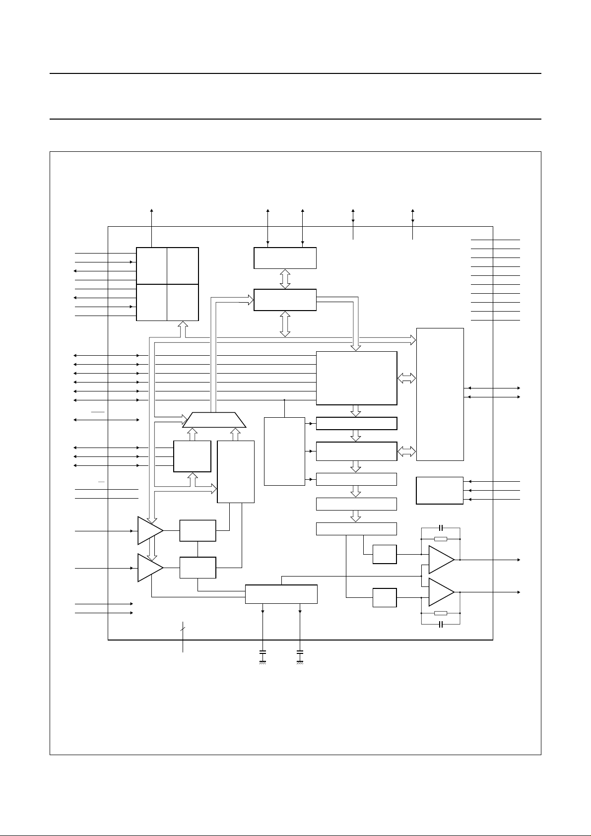
BLOCK DIAGRAM
handbook, full pagewidth
V
SSX
XTAL1b
XTAL2b
V
DDX
V
DDA3
XTAL2a
XTAL1a
V
SSA3
GP2/DO
GP3/WSO
GP4/BCKO
GP1/DI
GP0/BCKI
GP5/WSI
24 (19)
25 (20)
26 (21)
28 (22)
52 (39)
53 (40)
54 (41)
55 (42)
63 (4)
1 (5)
2 (6)
13 (14)
17 (16)
15 (15)
OSC
48 MHz
OSC
ADC
CLK
27
TIMING
ANALOG
PLL
D+
8 (9) 6 (8)
ANALOG FRONT-END
USB-PROCESSOR
D−
P0.7 to P0.0
7, 5, 3, 64,
62, 60, 58, 56
DIGITAL I/O
P2.0 to P2.7
14, 16, 18, 20,
22, 23, 29, 30
MICRO-
CONTROLLER
(10) 9
(11) 10
(12) 11
(13) 12
(23) 32
(24) 33
(29) 38
(30) 39
(33) 42
(35) 44
(17) 19
(18) 21
V
V
V
V
V
V
V
V
V
V
SCL
SDA
DDI
SSI
SSE
DDE
DDO
SSO
DDA1
SSA1
DDA2
SSA2
PSEN
WS
BCK
ALE
VINL
VINR
VRN
VRP
31
57 (1)
DA
59 (2)
61 (3)
48
EA
50
43 (34)
47 (36)
49 (37)
51 (38)
PGA
PGA
INTERFACE
MUX
SAMPLE
I2S-BUS
LEFT
Σ∆ ADC
DECIMATOR
FILTER
FREQUENCY
GENERATOR
UDA1325
RIGHT
Σ∆ ADC
REFERENCE VOLTAGE
45, 46 41 (32) 40 (31)
n.c.
V
ref(AD)
V
FIFO
AUDIO FEATURE
PROCESSING DSP
UPSAMPLE FILTERS
VARIABLE HOLD REGISTER
3rd-ORDER NOISE SHAPER
ref(DA)
LEFT
DAC
RIGHT
DAC
TEST
CONTROL
BLOCK
−
+
+
−
(7) 4
(26) 35
(27) 36
(25) 34
(28) 37
MGM108
SHTCB
TC
RTCB
VOUTL
VOUTR
The pin numbers given in parenthesis refer to the SDIP42 version.
Fig.1 Block diagram (QFP64 package).
1999 May 10 5
Page 6

Philips Semiconductors Preliminary specification
Universal Serial Bus (USB) CODEC UDA1325
PINNING
SYMBOL
PIN
QFP64
PIN
SDIP42
I/O DESCRIPTION
GP3/WSO 1 5 I/O general purpose pin 3 or word select output
GP4/BCKO 2 6 I/O general purpose pin 4 or bit clock output
P0.5 3 − I/O Port 0.5 of the microcontroller
SHTCB 4 7 I shift clock of the test control block (active HIGH)
P0.6 5 − I/O Port 0.6 of the microcontroller
D− 6 8 I/O negative data line of the differential data bus, conforms to the USB
standard
P0.7 7 − I/O Port 0.7 of the microcontroller
D+ 8 9 I/O positive data line of the differential data bus, conforms to the USB
standard
V
V
V
V
DDI
SSI
SSE
DDE
910−digital supply voltage for core
10 11 − digital ground for core
11 12 − digital ground for I/O pads
12 13 − digital supply voltage for I/O pads
GP1/DI 13 14 I/O general purpose pin 1 or data input
P2.0 14 − I/O Port 2.0 of the microcontroller
GP5/WSI 15 15 I/O general purpose pin 5 or word select input
P2.1 16 − I/O Port 2.1 of the microcontroller
GP0/BCKI 17 16 I/O general purpose pin 0 or bit clock input
P2.2 18 − I/O Port 2.2 of the microcontroller
SCL 19 17 I/O serial clock line I
2
C-bus
P2.3 20 − I/O Port 2.3 of the microcontroller
SDA 21 18 I/O serial data line I
2
C-bus
P2.4 22 − I/O Port 2.4 of the microcontroller
P2.5 23 − I/O Port 2.5 of the microcontroller
V
SSX
24 19 − crystal oscillator ground (48 MHz)
XTAL1b 25 20 I crystal input (analog; 48 MHz)
XTAL2b 26 21 O crystal output (analog; 48 MHz)
CLK 27 − O 48 MHz clock output signal
V
DDX
28 22 − supply crystal oscillator (48 MHz)
P2.6 29 − I/O Port 2.6 of the microcontroller
P2.7 30 − I/O Port 2.7 of the microcontroller
PSEN 31 − I/O program store enable (active LOW)
V
V
DDO
SSO
32 23 − supply voltage for operational amplifier
33 24 − operational amplifier ground
VOUTL 34 25 O voltage output left channel
TC 35 26 I test control input (active HIGH)
RTCB 36 27 I asynchronous reset input of the test control block (active HIGH)
VOUTR 37 28 O voltage output right channel
1999 May 10 6
Page 7

Philips Semiconductors Preliminary specification
Universal Serial Bus (USB) CODEC UDA1325
SYMBOL
V
DDA1
V
SSA1
V
ref(DA)
V
ref(AD)
V
DDA2
PIN
QFP64
38 29 − analog supply voltage 1
39 30 − analog ground 1
40 31 O reference voltage output DAC
41 32 O reference voltage output ADC
42 33 − analog supply voltage 2
PIN
SDIP42
I/O DESCRIPTION
VINL 43 34 I input signal left channel PGA
V
SSA2
44 35 − analog ground 2
n.c. 45 −−not connected
n.c. 46 −−not connected
VINR 47 36 I input signal right channel PGA
EA 48 −−external access (active LOW)
VRN 49 37 I negative reference input voltage ADC
ALE 50 −−address latch enable (active HIGH)
VRP 51 38 I positive reference input voltage ADC
V
DDA3
52 39 − supply voltage for crystal oscillator and analog PLL
XTAL2a 53 40 O crystal output (analog; ADC)
XTAL1a 54 41 I crystal input (analog; ADC)
V
SSA3
55 42 − crystal oscillator and analog PLL ground
P0.0 56 − I/O Port 0.0 of the microcontroller
DA 57 1 I data Input (digital)
P0.1 58 − I/O Port 0.1 of the microcontroller
WS 59 2 I word select Input (digital)
P0.2 60 − I/O Port 0.2 of the microcontroller
BCK 61 3 I bit clock Input (digital)
P0.3 62 − I/O Port 0.3 of the microcontroller
GP2/DO 63 4 I/O general purpose pin 2 or data output
P0.4 64 − I/O Port 0.4 of the microcontroller
1999 May 10 7
Page 8
Philips Semiconductors Preliminary specification
Universal Serial Bus (USB) CODEC UDA1325
handbook, full pagewidth
GP3/WSO
GP4/BCKO
P0.5
SHTCB
P0.6
D−
P0.7
D+
V
DDI
V
SSI
V
SSE
V
DDE
GP1/DI
P2.0
GP5/WSI
P2.1
GP0/BCKI
P2.2
SCL
56
28
DDX
V
SSA3
V
55
29
P2.6
XTAL1a
54
30
P2.7
P0.4
GP2/DO
P0.3
BCK
P0.2WSP0.1DAP0.0
64
63
62
61
60
59
58
57
1
2
3
4
5
6
7
8
9
23
P2.5
UDA1325H
24
25
SSX
V
XTAL1b
26
27
CLK
XTAL2b
10
11
12
13
14
15
16
17
18
19
20
21
22
P2.3
SDA
P2.4
XTAL2a
V
53
52
31
32
PSEN
V
DDA3
51
50
49
48
47
46
45
44
43
42
41
40
39
38
37
36
35
34
33
DDO
VRP
ALE
VRN
EA
VINR
n.c.
n.c.
V
SSA2
VINL
V
DDA2
V
ref(AD)
V
ref(DA)
V
SSA1
V
DDA1
VOUTR
RTCB
TC
VOUTL
V
SSO
MGL349
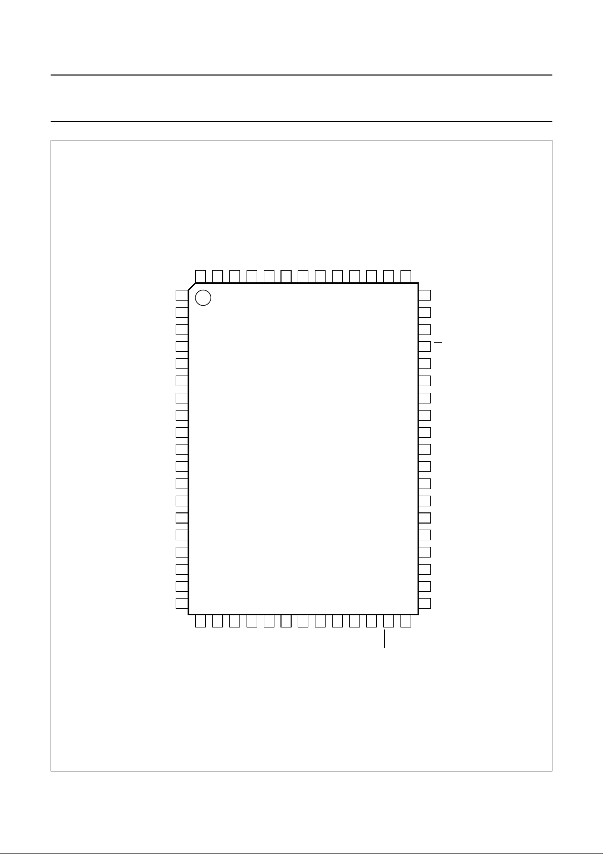
Fig.2 Pin configuration (QFP64 package).
1999 May 10 8
Page 9
Philips Semiconductors Preliminary specification
Universal Serial Bus (USB) CODEC UDA1325
FUNCTIONAL DESCRIPTION
The Universal Serial Bus (USB)
Data and power is transferred via the USB over a 4-wire
cable. The signalling occurs over two wires and
point-to-point segments. The signals on each segment are
differentially driven into a cable of 90 Ω intrinsic
impedance. The differential receiver features input
sensitivity of at least 200 mV and sufficient common mode
handbook, halfpage
GP3/WSO
GP4/BCKO
GP5/WSI
GP0/BCKI
DA
WS
BCK
GP2/DO
SHTCB
D−
D+
V
DDI
V
SSI
V
SSE
V
DDE
GP1/DI
SCL
SDA
V
SSX
XTAL1b
XTAL2b
1
2
3
4
5
6
7
8
9
10
11
12
13
14
15
16
17
18
19
20
UDA1325
MGM106
42
41
40
39
38
37
36
35
34
33
32
31
30
29
28
27
26
25
24
23
2221
V
SSA3
XTAL1a
XTAL2a
V
DDA3
VRP
VRN
VINR
V
SSA2
VINL
V
DDA2
V
ref(AD)
V
ref(DA)
V
SSA1
V
DDA1
VOUTR
RTCB
TC
VOUTL
V
SSO
V
DDO
V
DDX
rejection.
The analog front-end
The analog front-end is an on-chip generic USB
transceiver. It is designed to allow voltage levels up to V
DD
from standard or programmable logic to interface with the
physical layer of the USB. It is capable of receiving and
transmitting serial data at full speed (12 Mbits/s).
The USB processor
The USB processor forms the interface between the
analog front-end, the ADIF, the ADAC and the
microcontroller. The USB processor consists of:
• A bit clock recovery circuit
• The Philips Serial Interface Engine (PSIE)
• The Memory Management Unit (MMU)
• The Audio Sample Redistribution (ASR) module.
Bit clock recovery
The bit clock recovery circuit recovers the clock from the
incoming USB data stream using four times over-sampling
principle. It is able to track jitter and frequency drift
specified by the USB specification.
Philips Serial Interface Engine (PSIE)
The Philips SIE implements the full USB protocol layer.
It translates the electrical USB signals into data bytes and
control signals. Depending upon the USB device address
and the USB endpoint address, the USB data is directed
to the correct endpoint buffer. The data transfer could be
of bulk, isochronous, control or interrupt type.
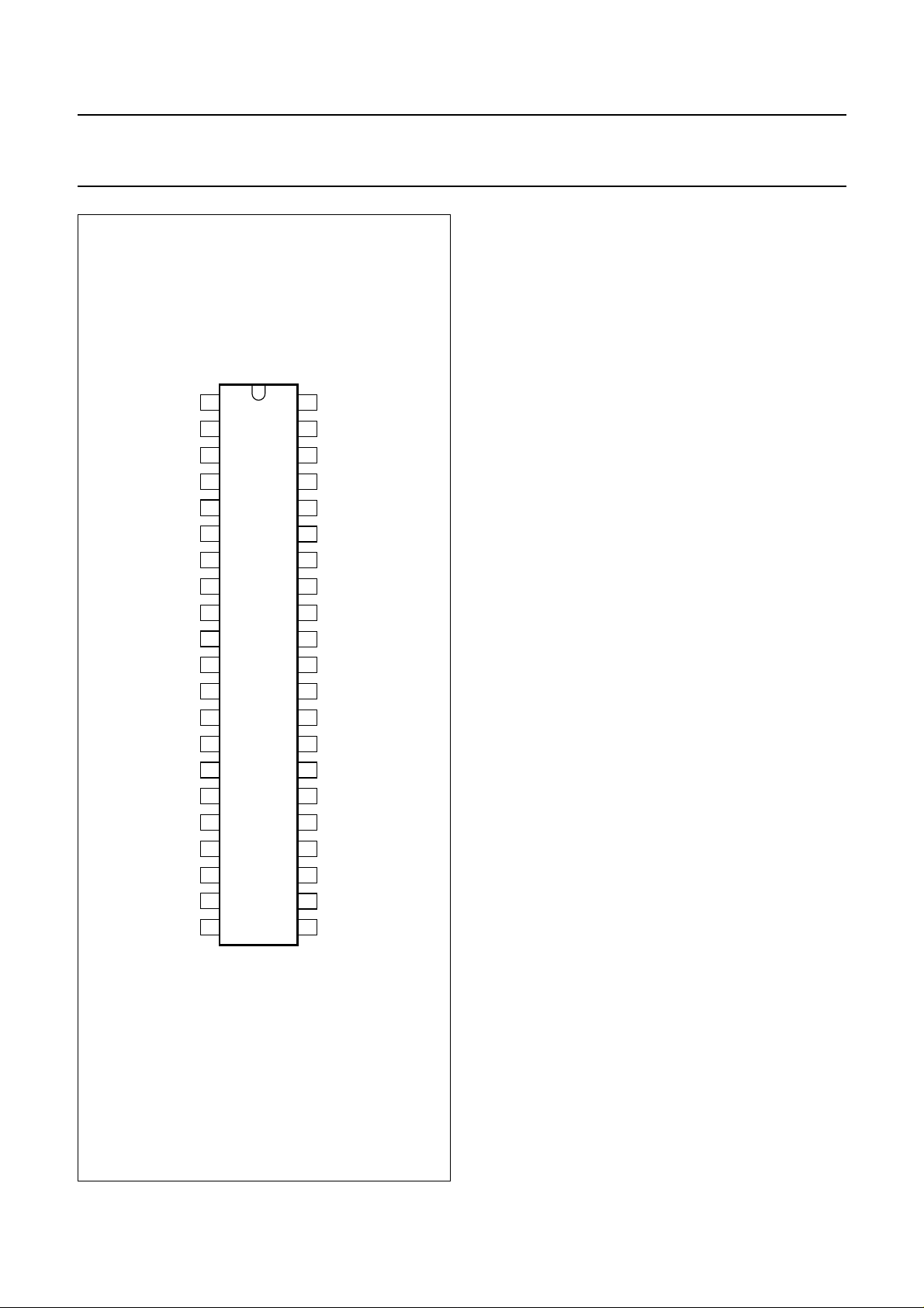
Fig.3 Pin configuration (SDIP42 package).
1999 May 10 9
The functions of the PSIE include: synchronization pattern
recognition, parallel/serial conversion, bit
stuffing/de-stuffing, CRC checking/generation, PID
verification/generation, address recognition and
handshake evaluation/generation.
The amount of bytes/packet on all endpoints is limited by
the PSIE hardware to 8 bytes/packet, except for both
isochronous endpoints (336 bytes/packet).
Page 10

Philips Semiconductors Preliminary specification
Universal Serial Bus (USB) CODEC UDA1325
Memory Management Unit (MMU) and integrated RAM
The MMU and integrated RAM handle the temporary data
storage of all USB packets that are received or sent over
the bus.
The MMU and integrated RAM handle the differences
between data rate of the USB and the application allowing
the microcontroller to read and write USB packets at its
own speed.
The audio data is transferred via an isochronous data sink
endpoint or source endpoint and is stored directly into the
RAM. Consequently, no handshaking mechanism is used.
Audio Sample Redistribution (ASR)
The ASR reads the audio samples from the MMU and
integrated RAM and distributes these samples equidistant
over a 1 ms frame period. The distributed audio samples
are translated by the digital I/O module to standard I
2
S-bus
format or 16, 18 or 20 bits LSB-justified I2S-bus format.
The ASR generates the bit clock output (BCKO) and the
Word Select Output signal (WSO) of the I2S output.
The 80C51 microcontroller
The microcontroller receives the control information
selected from the USB by the USB processor. It can be
used for handling the high-level USB protocols and the
user interfaces. The microcontroller does not handle the
audio stream.
The major task of the software process that is mapped
upon the microcontroller, is to control the different modules
of the UDA1325 in such a way that it behaves as a USB
device.
The embedded 80C51 microcontroller is compatible with
the 80C51 family of microcontrollers described in the
80C51 family single-chip 8-bit microcontrollers of “Data
Handbook IC20”, which should be read in conjunction with
this data sheet.
The Analog-to-Digital Interface (ADIF)
The ADIF is used for sampling an analog input signal from
a microphone or line input and sending the audio samples
to the USB interface. The ADIF consists of a stereo
Programmable Gain Amplifier (PGA), a stereo
Analog-to-Digital Converter (ADC) and Decimation Filters
(DFs). The sample frequency of the ADC is determined by
the ADC clock (see Section “The clock source of the
analog-to-digital interface”). The user can also select a
digital serial input instead of an analog input. In this event
the sample frequency is determined by the continuous WS
clock with a range between 5 to 55 kHz. Digital serial input
is possible with four formats (I
2
S-bus, 16, 18 or 20 bits
LSB-justified).
Programmable Gain Amplifier circuit (PGA)
This circuit can be used for a microphone or line input.
The input audio signals can be amplified by seven different
gains (−3 dB, 0 dB, 3 dB, 9 dB, 15 dB, 21 dB and 27 dB).
The gain settings are given in Table 17.
The Analog-to-Digital Converter (ADC)
The stereo ADC of the UDA1325 consists of two 3rd-order
Sigma-Delta modulators. They have a modified
Ritchie-coder architecture in a differential switched
capacitor implementation. The oversampling ratio is 128.
Both ADCs can be switched off in power saving mode (left
and right separate). The ADC clock is generated by the
analog PLL or the ADC oscillator.
The Decimation Filter (DF)
The decimator filter converts the audio data from 128f
s
down to 1fs with a word width of 8, 16 or 24 bits. This data
can be transmitted over the USB as mono or stereo in
1, 2 or 3 bytes/sample. The decimator filters are clocked
by the ADC clock.
The internal ROM size is 12 kbyte. The internal RAM size
is 256 byte. A Watchdog Timer is not integrated.
1999 May 10 10
Page 11
Philips Semiconductors Preliminary specification
Universal Serial Bus (USB) CODEC UDA1325
The clock source of the analog-to-digital interface
The clock source of the ADIF is the analog PLL or the ADC oscillator. The preferred clock source can be selected.
The ADC clock used for the ADC and decimation filters is obtained by dividing the clock signal coming from the analog
PLL or from the ADC oscillator by a factor Q.
Using the analog PLL the user can select 3 basic APLL clock frequencies (see Table 1).
By connecting the appropriate crystal the user can choose any clock signal between 8.192 and 14.08 MHz via the ADC
oscillator.
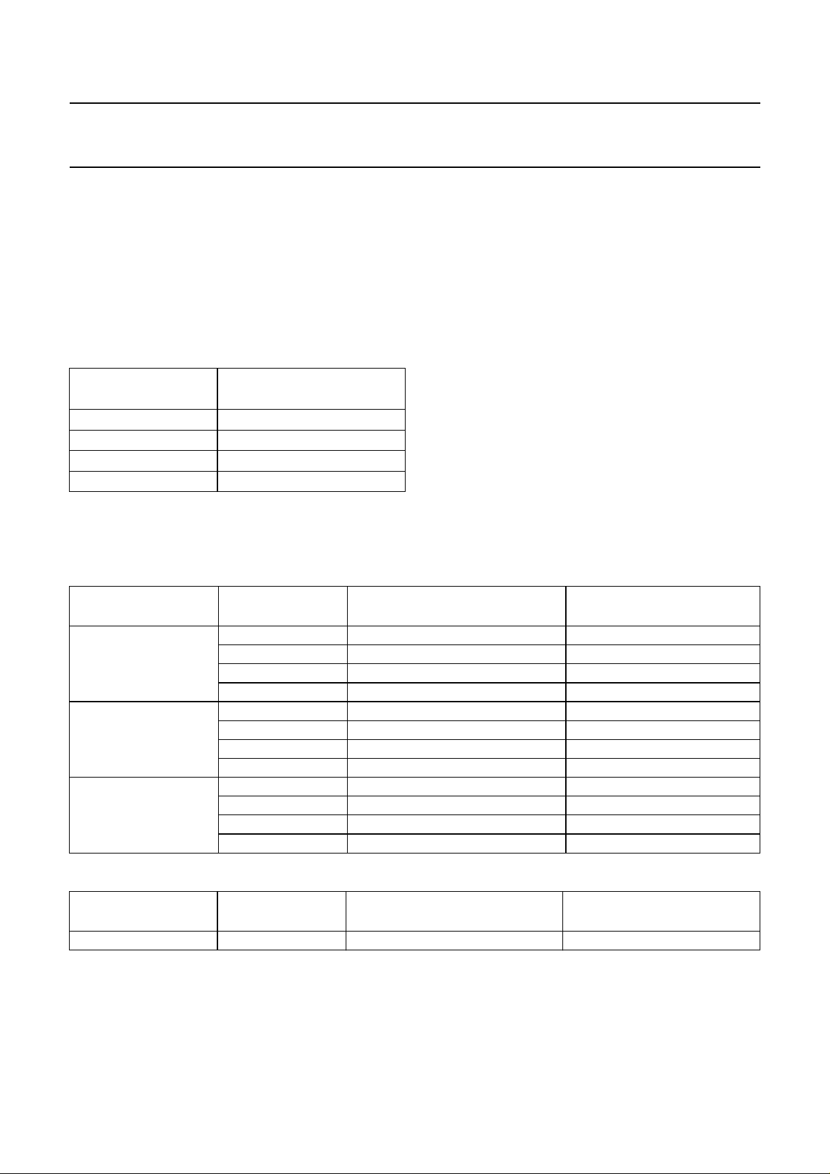
Table 1 The analog PLL clock output frequencies
FCODE (1 AND 0)
APLL CLOCK
FREQUENCY (MHz)
00 11.2896
01 8.1920
10 12.2880
11 11.2896
The dividing factor Q can be selected via the microcontroller. With this dividing factor Q the user can select a range of
ADC clock signals allowing several different sample frequencies (see Table 2).
Table 2 ADC clock frequencies and sample frequencies based upon using the APLL as a clock source
APLL CLOCK
FREQUENCY (MHz)
DIVIDE FACTOR Q ADC CLOCK FREQUENCY (MHz) SAMPLE FREQUENCY (kHz)
8.1920 1 4.096 32
2 2.048 16
4 1.024 8
8 0.512 (not supported) 4 (not supported)
11.2896 1 5.6448 44.1
2 2.8224 22.05
4 1.4112 11.025
8 0.7056 5.5125
12.2880 1 6.144 48
2 3.072 24
4 1.536 12
8 0.768 6
Table 3 ADC clock frequencies and sample frequencies based upon using the OSCAD as a clock source
OSCAD CLOCK
FREQUENCY (MHz)
(1)
f
osc
DIVIDE FACTOR Q ADC CLOCK FREQUENCY (MHz) SAMPLE FREQUENCY (kHz)
(2)
Q
f
/(2Q) f
osc
/(256Q)
osc
Notes
1. The oscillator frequency (and therefore the crystal) of OSCAD must be between 8.192 and 14.08 MHz.
2. The Q factor can be 1, 2, 4 or 8.
3. Sample frequencies below 5 kHz and above 55 kHz are not supported.
1999 May 10 11
(3)
Page 12

Philips Semiconductors Preliminary specification
Universal Serial Bus (USB) CODEC UDA1325
The Asynchronous Digital-to-Analog Converter (ADAC)
The ADAC receives audio data from the USB processor or
from the digital I/O-bus. The ADAC is able to reconstruct
the sample clock from the rate at which the audio samples
arrive and handles the audio sound processing. After the
processing, the audio signal is upsampled, noise-shaped
and converted to analog output voltages capable of driving
a line output.
The ADAC consists of:
• A Sample Frequency Generator (SFG)
• FIFO registers
• An audio feature processing DSP
• Two digital upsampling filters and a variable hold
register
• A digital Noise Shaper (NS)
• A Filter Stream DAC (FSDAC) with integrated filter and
line output drivers.
The Sample Frequency Generator (SFG)
The SFG controls the timing signals for the asynchronous
digital-to-analog conversion. By means of a digital PLL,
the SFG automatically recovers the applied sampling
frequency and generates the accurate timing signals for
the audio feature processing DSP and the upsampling
filters.
The lock time of the digital PLL can be chosen (see
Table 8). While the digital PLL is not in lock, the ADAC is
muted. As soon as the digital PLL is in lock, the mute is
released as described in Section “Soft mute control”.
Table 4 Frequency domains for audio processing by the
DSP
DOMAIN SAMPLE FREQUENCY (kHz)
1 5to12
212to25
325to40
440to55
The upsampling filters and variable hold function
After the audio feature processing DSP two upsampling
filters and a variable hold function increase the
oversampling rate to 128f
.
s
The noise shaper
A 3rd-order noise shaper converts the oversampled data
to a noise-shaped bitstream for the FSDAC. The in-band
quantization noise is shifted to frequencies well above the
audio band.
The Filter Stream DAC (FSDAC)
The FSDAC is a semi-digital reconstruction filter that
converts the 1-bit data stream of the noise shaper to an
analog output voltage. The filter coefficients are
implemented as current sources and are summed at
virtual ground of the output operational amplifier. In this
way very high signal-to-noise performance and low clock
jitter sensitivity is achieved. A post filter is not needed
because of the inherent filter function of the DAC.
On-board amplifiers convert the FSDAC output current to
an output voltage signal capable of driving a line output.
First-In First-Out (FIFO) registers
The FIFO registers are used to store the audio samples
temporarily coming from the USB processor or from the
digital I/O input. The use of a FIFO (in conjunction with the
SFG) is necessary to remove all jitter present on the
incoming audio signal.
The sound processing DSP
A DSP processes the sound features. The control and
mapping of the sound features is explained in Section
“Controlling the playback features of the ADAC”.
Depending on the sampling rate (f
) the DSP knows four
s
frequency domains in which the treble and bass are
regulated. The domain is chosen automatically.
1999 May 10 12
Page 13

Philips Semiconductors Preliminary specification
Universal Serial Bus (USB) CODEC UDA1325
USB ENDPOINT DESCRIPTION
The UDA1325 has following six endpoints:
• USB control endpoint 0
• USB control endpoint 1
• USB status interrupt endpoint 1
• USB status interrupt endpoint 2
• Isochronous data sink endpoint
• Isochronous data source endpoint.
Table 5 Endpoint description
ENDPOINT
NUMBER
0 0 control (default) out 8
1 2 control out 8
2 4 interrupt in 8
3 5 interrupt in 8
4 6 isochronous out out 336
5 7 isochronous in in 336
CONTROLLING THE PLAYBACK FEATURES
Controlling the playback features of the ADAC
The exchange of control information between the microcontroller and the ADAC is accomplished through a serial
hardware interface comprising the following pins:
L3_DATA: microcontroller interface data line
L3_MODE: microcontroller interface mode line
L3_CLK: microcontroller interface clock line.
See also the description of Port 3 of the 80C51 microcontroller.
ENDPOINT
INDEX
1in8
3in8
ENDPOINT TYPE DIRECTION
MAX. PACKET
SIZE (BYTES)
Information transfer through the microcontroller bus is organized in accordance with the so-called ‘L3’ format, in which
two different modes of operation can be distinguished; address mode and data transfer mode.
The address mode is required to select a device communicating via the L3-bus and to define the destination registers
for the data transfer mode. Data transfer for the UDA1325 can only be in one direction, from microcontroller to ADAC to
program its sound processing features and other functional features.
DDRESS MODE
A
The address mode is used to select a device (in this case the ADAC) for subsequent data transfer and to define the
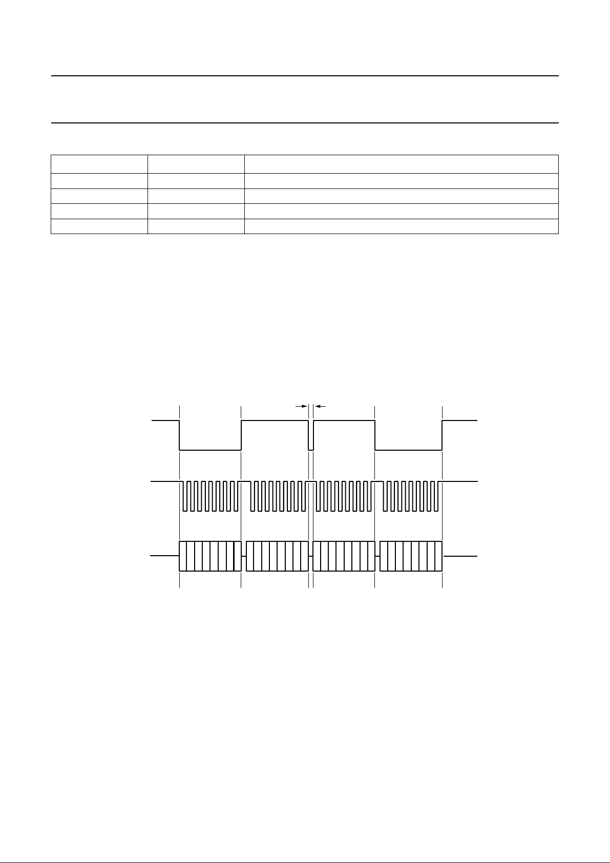
destination registers. The address mode is characterized by L3_MODE being LOW and a burst of 8 pulses on L3_CLK,
accompanied by 8 data bits on L3_DATA. Data bits 0 and 1 indicate the type of the subsequent data transfer as shown
in Table 6.
1999 May 10 13
Page 14
Philips Semiconductors Preliminary specification
Universal Serial Bus (USB) CODEC UDA1325
Table 6 Selection of data transfer type
BIT1 BIT0 DATA TRANSFER TYPE
0 0 audio feature registers (volume left, volume right, bass and treble)
0 1 not used
1 0 control registers
1 1 not used
Data bits 7 to 2 represent a 6-bit device address, with bit 7 being the MSB and bit 2 the LSB. The address of the ADAC
is 000101 (bits 7 to 2). In the event that the ADAC receives a different address, it will deselect its microcontroller interface
logic.
D
AT A TRANSFER MODE
The selection preformed in the address mode remains active during subsequent data transfers, until the ADAC receives
a new address command. The data transfer mode is characterized by L3_MODE being HIGH and a burst of 8 pulses on
L3_CLK, accompanied by 8 data bits. All transfers are bitwise, i.e. they are based on groups of 8 bits. Data will be stored
in the ADAC after the eight bit of a byte has been received. The principle of a multibyte transfer is illustrated in the figure
below.
t
dbook, full pagewidth
L3MODE
L3CLOCK
L3DATA
address
ROGRAMMING THE SOUND PROCESSING AND OTHER FEATURES
P
halt
addressdata byte #1 data byte #2
MGD018
The sound processing and other feature values are stored in independent registers. The first selection of the registers is
achieved by the choice of data transfer type. This is performed in the address mode, bits 1 and 0 (see Table 6).
The second selection is performed by bit 7 and/or bit 6 of the data byte depending of the selected data transfer type.
Data transfer type ‘audio feature registers’
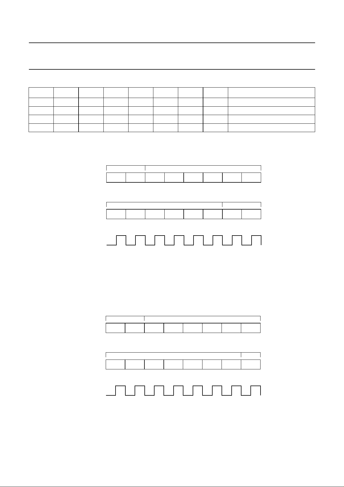
When the data transfer type ‘audio feature registers’ is selected 4 audio feature registers can be selected depending on
bits 7 and 6 of the data byte (see Table 7).
1999 May 10 14
Page 15
Philips Semiconductors Preliminary specification
Universal Serial Bus (USB) CODEC UDA1325
Table 7 ADAC audio feature registers
BIT7 BIT6 BIT5 BIT4 BIT3 BIT2 BIT1 BIT0 REGISTER
0 0 VR5 VR4 VR3 VR2 VR1 VR0 volume right
0 1 VL5 VL4 VL3 VL2 VL1 VL0 volume left
1 0 X BB4 BB3 BB2 BB1 BB0 bass
1 1 X TR4 TR3 TR2 TR1 TR0 treble
The sequence for controlling the ADAC audio feature registers via the L3-bus is given in the figure below.
book, full pagewidth
(L3_MODE = LOW)
L3_DATA
(L3_MODE = HIGH)
L3_DATA
L3_CLK
DATA_TRANSFER_TYPE
0
bit 0
X
bit 0
0 1 0 1
LEFT VOLUME; TREBLE
RIGHT VOLUME; BASS
X X X X
DEVICE ADDRESS = $5
0 0 0
X
bit 7
REGISTER
ADDRESS
X X
bit 7
MGS270
Data transfer type ‘control registers’
When the data transfer type ‘control registers’ is selected 2 general control registers can be selected depending on bit 7
of the data byte (see Table 7).
The sequence for controlling the ADAC control registers via the L3-bus is given in the figure below.
book, full pagewidth
(L3_MODE = LOW)
L3_DATA
(L3_MODE = HIGH)
L3_DATA
DATA_TRANSFER_TYPE
0
bit 0
X
bit 0
1 1 0 1
X X X X
DEVICE ADDRESS = $5
0 0 0
X
bit 7
REGISTER
ADDRESSDATA OF THE CONTROL REGISTER
X X
bit 7
L3_CLK
1999 May 10 15
MGS269
Page 16

Philips Semiconductors Preliminary specification
Universal Serial Bus (USB) CODEC UDA1325
Table 8 ADAC general control registers
REGISTER BIT DESCRIPTION V ALUE COMMENT
Control register 0 0 reset ADAC 0 = not reset
1 = reset
1 soft mute control 0 = not muted
1 = mutes
2 synchronous/asynchronous 0 = asynchronous
3 channel manipulation 0 = L -> L, R -> R
4 de-emphasis 0 = de-emphasis off
6 and 5 audio mode 00 = flat mode
7 selecting bit 0
Control register 1 1 and 0 serial I
3 and 2 digital PLL mode 00 = adaptive
4 digital PLL lock mode 0 = adaptive
6 and 5 digital PLL lock speed 00 = lock after 512 samples
7 selecting bit 1
1 = synchronous
1=L->R, R->L
1 = de-emphasis on
01 = min. mode
10 = min. mode
11 = max. mode
2
S-bus input format 00 = I2S-bus
01 = 16-bit LSB justified
10 = 18-bit LSB justified
11 = 20-bit LSB justified
01 = fix state 1
10 = fix state 2
11 = fix state 3
1 = fixed
01 = lock after 2048 samples
10 = lock after 4096 samples
11 = lock after 16348 samples
select 0
select 00
select 1
select 00
Soft mute control
When the mute (bit 1 of control register 0) is active for the playback channel, the value of the sample is decreased
smoothly to zero following a raised cosine curve. There are 32 coefficients used to step down the value of the data, each
one being used 32 times before stepping to the next. This amounts to a mute transition of 23 ms at f
the mute is released, the samples are returned to the full level again following a raised cosine curve with the same
coefficients being used in reversed order.
The mute, on the master channel is synchronized to the sample clock, so that operation always takes place on complete
samples.
1999 May 10 16
= 44.1 kHz. When
s
Page 17
Philips Semiconductors Preliminary specification
Universal Serial Bus (USB) CODEC UDA1325
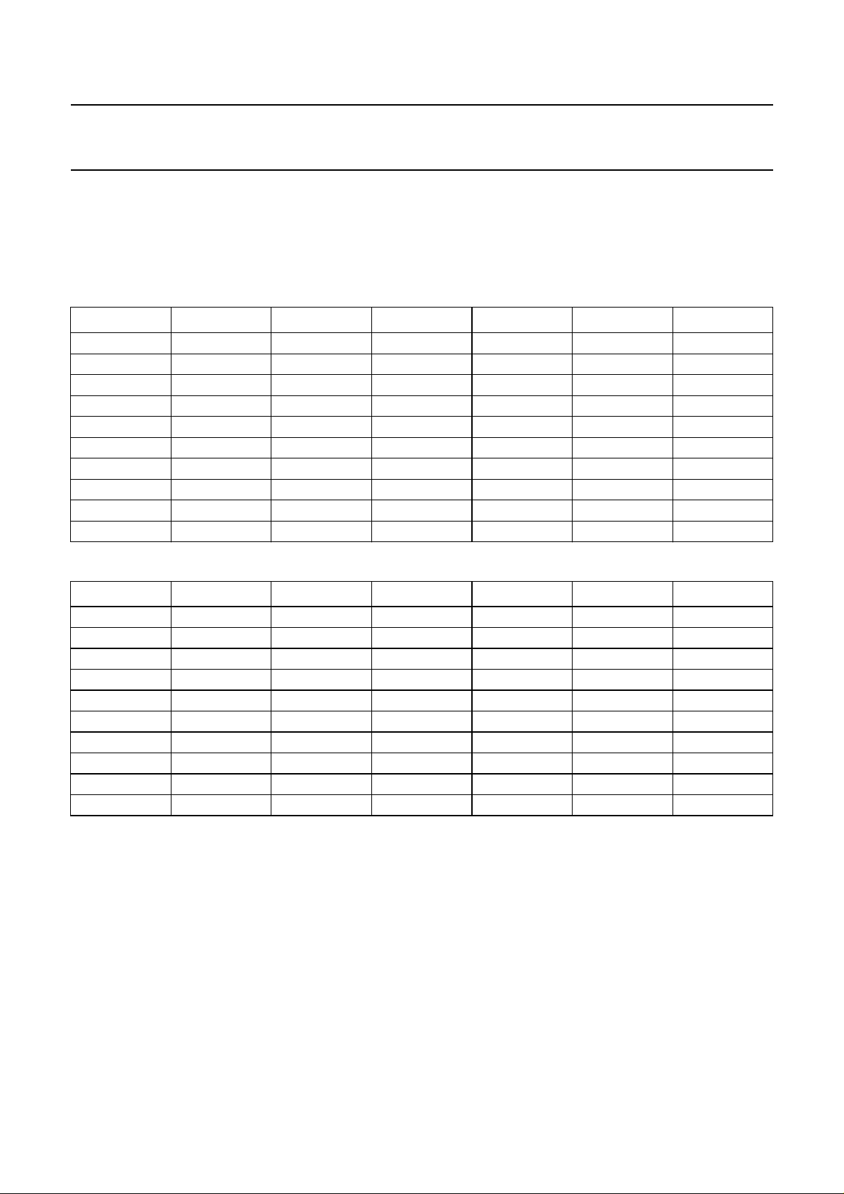
Volume control
The volume of the UDA1325 can be controlled from 0 dB down to −60 dB (in steps of 1 dB). Below −60 dB the audio
signal is muted (−∞ dB). The setting of 0 dB is always referenced to the maximum available volume setting. Independant
volume control of the left and right channel is possible (balance control).
Table 9 Volume settings right playback channel
VR5 VR4 VR3 VR2 VR1 VR0 VOLUME (dB)
0000000
0000010
000010−1
000011−2
000100−3
... ... ... ... ... ... ...
111100−59
111101−60
111110−∞
111111−∞
Table 10 Volume settings left playback channel
VL5 VL4 VL3 VL2 VL1 VL0 VOLUME (dB)
0000000
0000010
000010−1
000011−2
000100−3
... ... ... ... ... ... ...
111100−59
111101−60
111110−∞
111111−∞
1999 May 10 17
Page 18

Philips Semiconductors Preliminary specification
Universal Serial Bus (USB) CODEC UDA1325
Treble control
For the playback channel, treble can be regulated in three audio modes: minimum, flat and maximum mode. In flat mode
the audio is not influenced. In minimum and maximum mode, the treble range is from 0 to 6 dB in steps of 2 dB.
The programmable treble filter is implemented digitally and has a fixed corner frequency of 3000 Hz for the minimum
mode and 1500 Hz for the maximum mode. Because of the exceptional amount of programmable gain, treble should be
used with adequate prior attenuation, using volume control.
Table 11 Treble settings
TR4 TR3 TR2 TR1 TR0
FLAT SET MIN. SET MAX. SET
00000000
00001000
00010000
00011000
00100022
00101022
00110022
00111022
01000044
01001044
01010044
01011044
01100066
01101066
01110066
01111066
... ... ... ... ... 0 6 6
11111066
TREBLE (dB)
Bass control
For the playback channel, bass can be regulated in three audio modes: minimum, flat and maximum mode. In flat mode
the audio is not influenced. In minimum mode the bass range is from 0 to approximately 14 dB in steps of 1.5 dB.
In maximum mode, the bass range is from 0 to approximately 24 dB in steps of 2 dB. The programmable bass filters are
implemented digitally and have a fixed corner frequency of 100 Hz for the minimum mode and 75 Hz for the maximum
mode. Because of the exceptional amount of programmable gain, bass should be used with adequate prior attenuation,
using volume control.
1999 May 10 18
Page 19

Philips Semiconductors Preliminary specification
Universal Serial Bus (USB) CODEC UDA1325
Table 12 Bass boost settings
BB4 BB3 BB2 BB1 BB0
FLAT SET MIN. SET MAX. SET
00000000
00001000
00010000
00011000
0010001.11.7
0010101.11.7
0011002.43.6
0011102.43.6
0100003.75.4
0100103.75.4
0101005.27.4
0101105.27.4
0110006.89.4
0110106.89.4
0111008.411.3
0111108.411.3
10000010.2 13.3
10001010.2 13.3
10010011.915.2
10011011.915.2
10100013.7 17.3
10101013.7 17.3
10110013.7 19.2
10111013.7 19.2
11000013.7 21.2
11001013.7 21.2
11010013.7 23.2
11011013.7 23.2
... ... ... ... ... 0 13.7 23.2
11111013.7 23.2
BASS (dB)
De-emphasis
De-emphasis is controlled by bit 4 of control register 0. The de-emphasis filter can be switched on or off. The digital
de-emphasis filter is dimensioned to produce the de-emphasis frequency characteristics for the sample rate 44.1 kHz.
De-emphasis is synchronized to the sample clock, so that operation always takes place on complete samples.
1999 May 10 19
Page 20
Philips Semiconductors Preliminary specification
Universal Serial Bus (USB) CODEC UDA1325
Filter characteristics playback channel
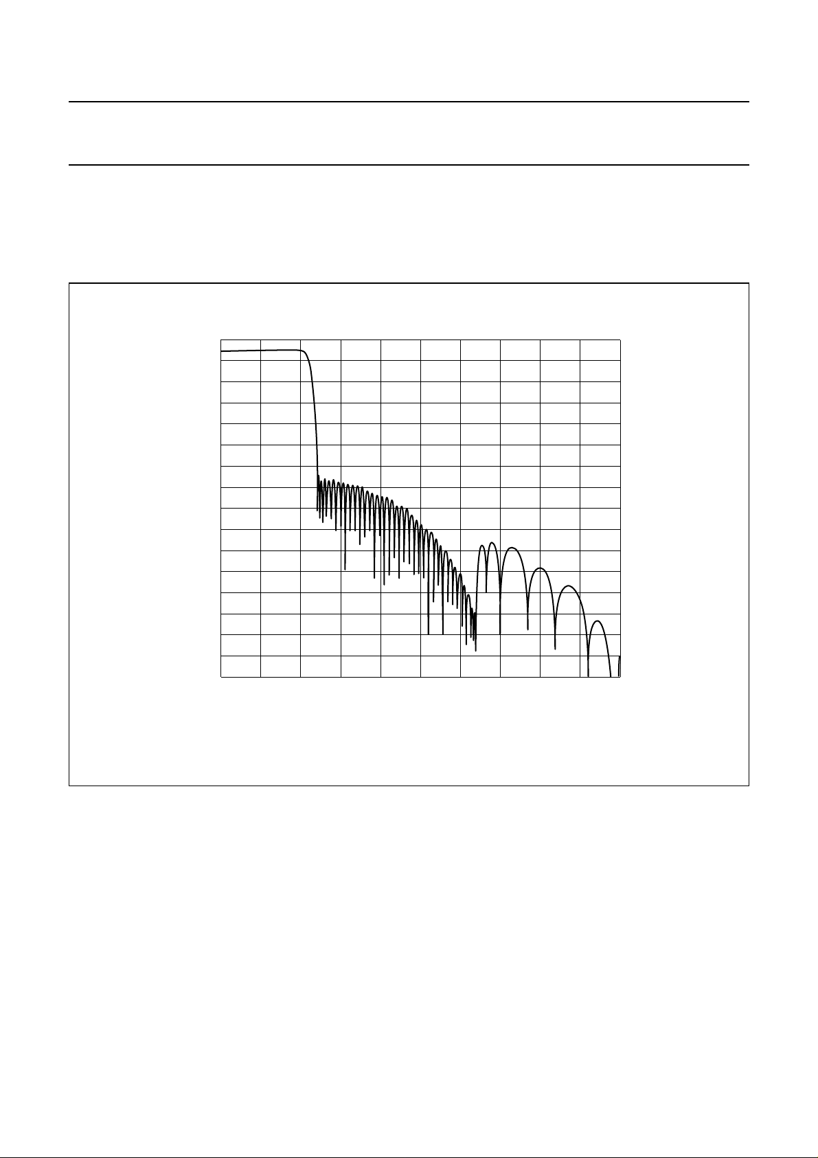
The overall filter characteristic of the UDA1325 in flat mode is given in Fig.4 (de-emphasis off). The overall filter
characteristic of the UDA1325 includes the filter characteristics of the DSP in flat mode plus the filter characteristic of the
FSDAC (fs= 44.1 kHz)
handbook, full pagewidth
volume
(dB)
−100
−120
−140
−160
−0
−20
−40
−60
−80
MGM110
10 20 30 40 50 60 70 80 90 1000
f (kHz)
Fig.4 Overall filter characteristics of the UDA1325.
1999 May 10 20
Page 21
Philips Semiconductors Preliminary specification
Universal Serial Bus (USB) CODEC UDA1325
DSP extension port for enhanced playback audio processing
An external DSP can be used for adding extra sound processing features via the I2S inputs and outputs of the digital I/O
module. The UDA1325 supports the standard I2S-bus data protocol and the LSB-justified serial data input format with
word lengths of 16, 18 and 20 bits. Using the 4-pin digital I/O option the UDA1325 device acts as a master, controlling
the BCKO and WSO signals. Using the 6-pin digital I/O option GP2, GP3 and GP4 are output pins (master) and GP0,
GP1 and GP5 are input pins (slave).
The period of the WSO signal is determined by the number of samples in the 1 ms frame of the USB. This implies that
the WSO signal does not have a constant time period, but is jittery.
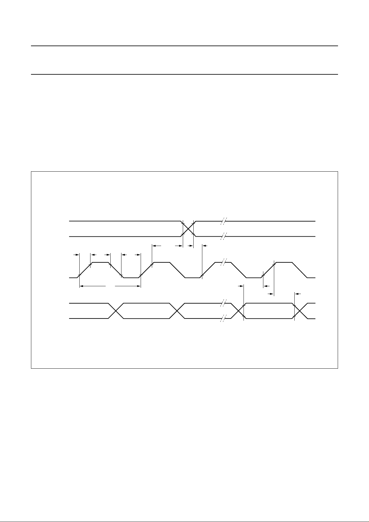
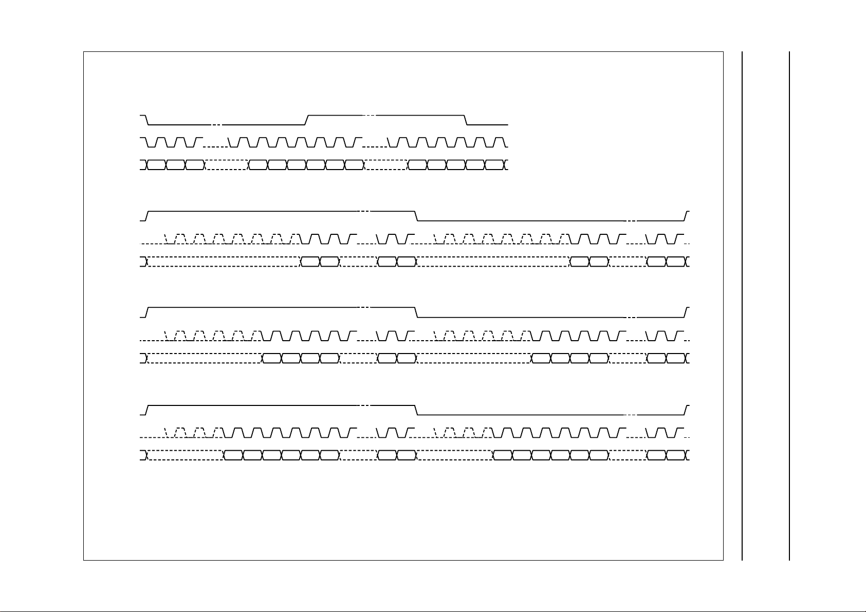
The characteristic timing of the I2S-bus signals is illustrated in Figs 5 and 6.
handbook, full pagewidth
WS
BCK
DATA
t
r
t
BCK(H)
T
cy
RIGHT
t
f
t
s;WS
t
BCK(L)
t
h;WS
LSB MSB
Fig.5 Timing of digital I/O input signals.
t
s;DAT
LEFT
t
h;DAT
MGK003
1999 May 10 21
Page 22
This text is here in white to force landscape pages to be rotated correctly when browsing through the pdf in the Acrobat reader.This text is here in
b
_white to force landscape pages to be rotated correctly when browsing through the pdf in the Acrobat reader.This text is here inThis text is here in
white to force landscape pages to be rotated correctly when browsing through the pdf in the Acrobat reader. white to force landscape pages to be ...
1999 May 10 22
ook, full pagewidth
Philips Semiconductors Preliminary specification
Universal Serial Bus (USB) CODEC UDA1325
WS
BCK
DATA
WS
BCK
DATA
WS
BCK
DATA
WS
BCK
LEFT
>=8 >=8
MSB B2 MSBLSB LSB MSBB2
LEFT
MSB LSBB2
LEFT
MSB B2 B3 B4
LEFT
RIGHT
1516 1
321321
LSB
2
S-BUS
INPUT FORMAT I
2
B15
LSB-JUSTIFIED FORMAT 16 BITS
215161718 1
B17
LSB-JUSTIFIED FORMAT 18 BITS
2151617181920 1
RIGHT
MSB LSBB2 B15
RIGHT
MSB B2 B3 B4
RIGHT
B17
21516 1
215161718 1
LSB
2151617181920 1
DATA
MSB B2 B3 B4 B5 B6
LSB
B19
LSB-JUSTIFIED FORMAT 20 BITS
Fig.6 Input formats.
MSB B2 B3 B4 B5 B6
B19
LSB
MGK002
Page 23
Philips Semiconductors Preliminary specification
Universal Serial Bus (USB) CODEC UDA1325
PORT DEFINITION 80C51
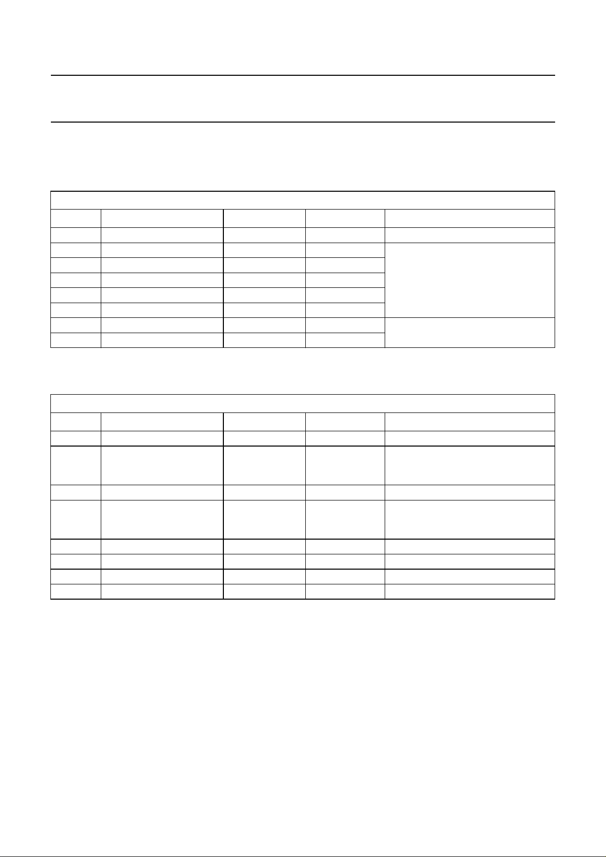
Port 1
Table 13 Port 1 of the 80C51 microcontroller
8 BIT PORT 1
BIT FUNCTION LOW HIGH COMMENT
1.0 ADAC_error no error error
1.1 GP1 general purpose pins
1.2 GP2
1.3 GP3
1.4 GP4
1.5 GP5
2
1.6 SCL I
1.7 SDA
C-bus
Port 3
Table 14 Port 3 of the 80C51 microcontroller
8 BIT PORT 3
BIT FUNCTION LOW HIGH COMMENT
3.0 ASR_error no error error
3.1 PSIE_MMU_SUSPEND no suspend suspend suspend input from USB interface
during normal operation or input from
restart circuit
3.2 GP0 (INT0_N) general purpose pin
3.3 PSIE_MMU_INT (INT1_N) interrupt input from USB interface
during normal operation or input from
restart circuit
3.4 PSIE_MMU_READY
3.5 L3_MODE
3.6 L3_CLK
3.7 L3_DATA
1999 May 10 23
Page 24
Philips Semiconductors Preliminary specification
Universal Serial Bus (USB) CODEC UDA1325
MEMORY AND REGISTER SPACE 80C51
Overview registers
Table 15 Register location and recommended values
after Power-on reset
ADDRESS REGISTER
RESET
VALUE
0800h PGA gain 09
0801h ADIF control 5C
1000h clock shop settings 00
1001h reset control and APLL settings 00
1002h IO selection register 01
1003h power control 00
2000h ASR settings 8B
4000h data register PSIE
4001h command register PSIE
Table 16 Special function register location
ADDRESS REGISTER
RESET
VALUE
CPU registers
81h SP
82h DPL
83h DPH
D0h PSW
E0h ACC
F0h B
Interrupt registers
A8h IE 00h
B8h IP 00h
ADDRESS REGISTER
RESET
VALUE
Port registers
80h P0 FFh
90h P1 FFh
A0h P2 FFh
B0h P3 FFh
2
I
C registers (SIO1 registers)
D8h S1CON 00h
D9h S1STA
DAh S1DAT
DBh S1ADR
Interrupts
The UDA1325 supports up to five (of maximal 7) interrupt
sources. Each interrupt source corresponds to an interrupt
vector in the CPU program memory address space:
Source 0: vector 0003h external interrupt 0 (INT0_N)
Source 1: vector 000Bh Timer 0 interrupt
Source 2: vector 0013h external interrupt 1 (INT1_N)
Source 3: vector 001Bh Timer 1 interrupt
Source 4: vector 0023h UART interrupt (not present)
Source 5: vector 002Bh Timer 2 interrupt (not present)
Source 6: vector 0033h I2C interrupt.
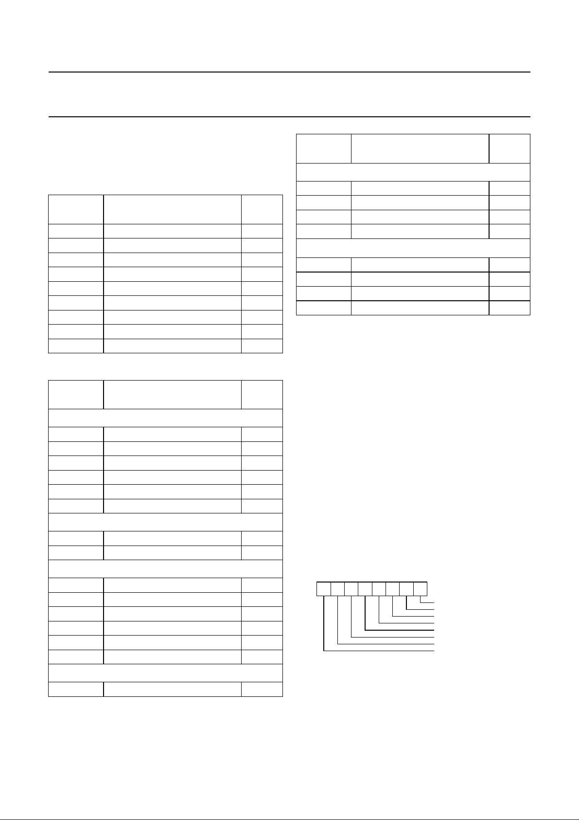
NTERRUPT ENABLE REGISTER (IE)
I
Each interrupt source can be individually enabled or
disabled by setting or clearing a bit in IE. This register also
contains a global interrupt enable bit (EA) which can be
cleared to disable all interrupts at once.
Timer 0 and Timer 1 registers
88h T01CON 00h
89h T01MOD 00h
8Ah T0L 00h
8Bh T1L 00h
8Ch T0h 00h
8Dh T1h 00h
PCON registers
87h PCON 00h
1999 May 10 24
76543210
0 0 0 0 0 0 0 0
Power On Value
EX0 (vector 0003h))
ET0 (vector 000Bh))
EX1 (vector 0013h)
ET1 (vector 001Bh)
ES0 (n.a.)
ET2 (n.a.)
ES1 (vector 0033h)
EA
Page 25

Philips Semiconductors Preliminary specification
Universal Serial Bus (USB) CODEC UDA1325
Internal registers
Table 17 PGA gain registers
ADDRESS REGISTER COMMENTS BIT VALUE
0800h PGA gain register reserved 7 X
PGA input selection 6 0 (do not change it)
PGA gain right channel 5, 4 and 3 000 = −3dB
001 = 0 dB
010 = 3 dB
011=9dB
100 = 15 dB
101 = 21 dB
110=27dB
111=27dB
PGA gain left channel 2, 1 and 0 000 = −3dB
001 = 0 dB
010 = 3 dB
011=9dB
100 = 15 dB
101 = 21 dB
110=27dB
111=27dB
Table 18 ADIF control registers
ADDRESS REGISTER COMMENTS BIT VALUE
0801h ADIF control register reserved 7 X
number of bits per audio sample
to be transmitted to the host
mono/stereo selection 4 0 = mono
selection audio input recording
channel
selection high-pass filter of
ADIF (DC-filter)
2
I
S-bus input serial input format
recording channel
6 and 5 00 = reserved
01 = 8 bits audio samples
10 = 16 bits audio samples
11 = 24 bits audio samples
1 = stereo
3 0 = digital serial audio input
1 = analog input
2 0 = high-pass filter off
1 = high-pass filter on
1 and 0 00 = I2S-bus
01 = 16-bit LSB justified
10 = 18-bit LSB justified
11 = 20-bit LSB justified
1999 May 10 25
Page 26

Philips Semiconductors Preliminary specification
Universal Serial Bus (USB) CODEC UDA1325
Table 19 Clock shop register
ADDRESS REGISTER COMMENTS BIT VALUE
1000h clock shop settings selection ADC clock source 7 0 = ADC clock from APLL
1 = ADC clock from OSCAD
divide factor Q 6 and 5 00 = ADC clock divided-by-1
01 = ADC clock divided-by-2
10 = ADC clock divided-by-4
11 = ADC clock divided-by-8
clock ADAC 4 0 = enable
1 = disable
clock 48 MHz internal 3 0 = enable
1 = disable
clock recovered by PSIE 2 0 = enable
1 = disable
ADC clock 1 0 = enable
1 = disable
OSCAD oscillator 0 0 = power on
1 = power off
Table 20 Reset control and APLL register
ADDRESS REGISTER COMMENTS BIT VALUE
1001h reset control and APLL
settings
fcode (1 and 0)
clock frequency selection APLL
reserved 5 X
reset ADAC 4 0 = reset off
reset MMU 3 0 = reset off
reset digital I/O-interface 2 0 = reset off
reset ADIF 1 0 = reset off
reserved 0 X
7 and 6 00 = 256 × 44.1 kHz
01 = 256 × 32 kHz
10 = 256 × 48 kHz
11 = 256 × 44.1 kHz
1 = reset on
1 = reset on
1 = reset on
1 = reset on
1999 May 10 26
Page 27

Philips Semiconductors Preliminary specification
Universal Serial Bus (USB) CODEC UDA1325
Table 21 I/O selection register
ADDRESS REGISTER COMMENTS BIT VALUE
1002h I/O selection register microcontroller control on
48 MHz oscillator
audio format 6 and 5 00 = 4-pins I
GP4 I/O if BIT0 = 1 4 0 = output
GP3 I/O if BIT0 = 1 3 0 = output
GP2 I/O if BIT0 = 1 2 0 = output
GP1 I/O if BIT0 = 1 1 0 = output
GP4 to GP1 function 0 0 = I
7 0 = UPC control disabled
(48 MHz oscillator is enabled)
1 = UPC control enabled
2
S
01 = 6-pins I2S
10 = 3-pins I2S (only input)
11 = 3-pins I2S (only input)
1 = input
1 = input
1 = input
1 = input
2
S usage
1 = general purpose usage
Table 22 Power control register
ADDRESS REGISTER COMMENTS BIT VALUE
1003h power control register
analog modules
suspend input selection for P3.1
of the microcontroller
7 0 = suspend from USB interface
connected to P3.1 during
normal operation
1 = suspend from restart circuit
connected to P3.1 (e.g. after
power-down)
interrupt input selection for
P3.3 (INT1_N) of the
microcontroller
6 0 = interrupt from USB
interface connected to P3.3
during normal operation
1 = interrupt from restart circuit
connected to P3.3 (e.g. after
power-down)
power APLL 5 0 = power on
1 = power off
power FSDAC 4 0 = power on
1 = power off
power ADC left 3 0 = power on
1 = power off
power ADC right 2 0 = power on
1 = power off
power PGA left 1 0 = power on
1 = power off
power PGA right 0 0 = power on
1 = power off
1999 May 10 27
Page 28

Philips Semiconductors Preliminary specification
Universal Serial Bus (USB) CODEC UDA1325
Table 23 ASR control register
ADDRESS REGISTER COMMENTS BIT VALUE
2000h ASR control register robust word clock 7 0 = off (not recommended)
1 = on (recommended)
2
serial I
digital I/O interface
phase inversion (on right mono
output)
bits per sample modi 3 and 2 00 = reserved
mono or stereo operation 1 0 = mono
ASR register start-up mode 0 0 = stop (e.g. at alternate
S-bus output format
6 and 5 00 = I2S-bus
01 = 16-bit LSB justified
10 = 18-bit LSB justified
11 = 20-bit LSB justified
4 0 = mono phase inversal off
1 = mono phase inversal on
01 = 8-bit audio
10 = 16-bit audio
11 = 24-bit audio
1 = stereo
setting with bandwidth equal to
zero)
1=go
START-UP BEHAVIOUR AND POWER MANAGEMENT
Start-up of the UDA1325
After power-on (of V
), an internal Power-on reset signal becomes HIGH after a certain RC time. This RC time is
DDA1
created by using the internal resistor (2 × 50 kΩ) divider for creating the reference voltage for the FSDAC in combination
with the capacitor connected externally to the V
V
DDA1
and V
. The RC time can be calculated using R = 25000 Ω and C = C
SSA1
pin. The FSDAC and the internal resistor divider are supplied by
REFDA
.
ref
During 20 ms after Power-on reset becomes HIGH the UDA1325 has to initiate the internal registers. During this
initialisation, the user should prevent indicating the ‘connected’ status to the USB-host. This can be done by forcing the
DP-line LOW (i.e. via one of the GP pins).
Power Management
The total current drawn from the USB supply (for i.e. bus-powered operation of the UDA1325 application) must be less
than 500 µA in suspend mode. In order to reach that low current target, the total power dissipation of the UDA1325 can
be reduced by disabling all internal clocks and switching off all internal analog modules.
Important note: In order to make use of power reduction (Power-down mode) and be able to restart after power-down, a
number of precautions must be taken!
1999 May 10 28
Page 29

Philips Semiconductors Preliminary specification
Universal Serial Bus (USB) CODEC UDA1325
AT INITIALISATION TIME
• Bit 7of the power control register (mux_ctrl_suspend) must be set to ‘1’, in order to connect the CLK_ON of the USB
processor with P3.1 of the microcontroller
• Bit 6 of the power control register (mux_ctrl_int1) must be set to ‘0’, in order to connect the PSIE_MMU_INT output pin
of the USB processor with P3.3 (INT1_N) of the microcontroller
• Bit 7of the I/O selection register must be set to ‘1’, in order to enable the power-on control of the 48 MHz crystal
oscillator automatically by the microcontroller.
I
N NORMAL OPERATION MODE
In normal operation working mode, a suspend can be initiated by the falling edge of the CLK_ON output signal of the
USB processor. This falling edge comes about 2 ms after the rising edge of the PSIE_MMU_SUSPEND output signal of
the USB processor. At this moment, several actions should be taken by the microcontroller:
• All analog modules of the UDA1325 must be switched off; this can be done by setting bits 5 to 0 of the power control
register to ‘1’ and bit 0 of the clock shop register to ‘1’
• Bit 6 of the power control register (mux_ctrl_int1) must be set to ‘1’, in order to awake from power-down by the
CLK_ON signal of the USB processor
• Put all GP pins in the high or low state (depending of how they are used in the UDA1325 application)
• Put the microcontroller in Power-down mode. This can be done via the PCON register of the microcontroller. This
results in an automatically switching off the 48 MHz crystal oscillator and with that all internal clocks (if they are
enabled).
On the rising edge of the CLK_ON output signal, the 48 MHz crystal oscillator will be switched on automatically and with
that all internal clocks (if they are enabled). At the same time, a counter starts counting for 2048 clock cycles (170 µs).
This time is necessary for stabilising the 48 MHz clock of the 48 MHz crystal oscillator.
When the counter reaches its end value (after 2048 cycles), a rising edge will be detected on the P3.3 (INT1_N) of the
microcontroller. At this moment, following actions should be taken by the microcontroller:
• The Power-down mode of the microcontroller must be switched off
• Re-initialise all GP pins
• All analog modules of the UDA1325 must be switched on; this can be done by setting bits 5 to 0 of the power control
register to ‘0’ and bit 0 of the clock shop register to ‘0’
• Bit 6 of the power control register (mux_ctrl_int1) must be set to ‘0’, in order to connect the PSIE_MMU_INT output pin
of the USB processor again with P3.3 (INT1_N) of the microcontroller.
The UDA1325 is now back in its normal operation mode and can be put back in power reduction mode by the falling edge
of the CLK_ON signal of the USB processor.
1999 May 10 29
Page 30

Philips Semiconductors Preliminary specification
Universal Serial Bus (USB) CODEC UDA1325
COMMAND SUMMARY
COMMAND NAME RECIPIENT CODING DATA PHASE
Initialization commands
Set address/enable device D0h write 1 byte
Read address/enable device D0h read 1 byte
Set endpoint enable device D8h write 1 byte
Read endpoint enable device D8h read 1 byte
Set mode device F3h write 1 byte
Data flow commands
Read interrupt register device F4h read 1 byte
Select endpoint control OUT 00h read 1 byte (optional)
control IN 01h read 1 byte (optional)
other endpoints 00h + endpoint index read 1 byte (optional)
Get endpoint status control OUT 40h read 1 byte
control IN 41h read 1 byte
other endpoints 40h + endpoint index read 1 byte
Set endpoint status control OUT 40h write 1 byte
control IN 41h write 1 byte
other endpoints 40h + endpoint index write 1 byte
Read buffer selected endpoint F0h read n bytes
Write buffer selected endpoint F0h write n bytes
Acknowledge setup selected endpoint F1h none
Clear buffer selected endpoint F2h none
Validate buffer selected endpoint FAh none
General commands
Read current frame number F5h read 1 or 2 bytes
1999 May 10 30
Page 31

Philips Semiconductors Preliminary specification
Universal Serial Bus (USB) CODEC UDA1325
COMMAND DESCRIPTIONS
Command procedure
This chapter describes the commands that can be used by
the microcontroller to control the USB processor. There
are three basic types of commands:
• Initialization commands
• Data flow commands
• General commands.
A command is represented by an 8 bit code. It can be
followed by one or more data write cycles or one or more
read cycles or a combination. The PSIE_MMU_READY
output connected to Port 3.4 of the microcontroller
indicates that the previous action (command write, data
read or data write) has completed. A new action can only
be initiated if PSIE_MMU_READY is TRUE. The data is
valid from the moment PSIE_MMU_READY becomes
TRUE.
The PSIE contains a number of interrupt registers, one for
each endpoint. Every time a transition occurs, the interrupt
flag for the involved endpoint is set. The PSIE_MMU_INT
connected to Port 3.3 is an OR function of all interrupt
registers.
Initialization commands
Initialization commands are used during the enumeration
process of the USB network. They are used to set the USB
assigned address, enable endpoints and select the
configuration of the device.
S
ET ADDRESS/ENABLE
Command: D0h.
Data: write 1 byte.
The set address/enable command is used to set the USB
assigned address and enable the function. The device
always powers up disabled and should be enabled after a
bus reset.
01234567
0
000 0000
Power On Value
Address
Enable
Table 24
BIT DESCRIPTION
Address the value written becomes
the device address
Enable a ‘1’ enables this function
EAD ADDRESS/ENABLE
R
Command: D0h.
Data: read 1 byte.
The read address/enable command is used to read the
USB assigned address and the enable bit of the device.
The format of the data phase is the same as for the set
address/enable command.
S
ET ENDPOINT ENABLE
Command: D8h.
Data: write 1 byte.
The set endpoint enable command is used to set the
enable bits for the non default endpoints.
76543210
XXXXXXX0
Power On Value
Enable
Reserved
If the enable bit is ‘1’, the non default endpoints are
enabled, if ‘0’, the non default endpoints are disabled.
The function then only responds to the default control
endpoint.
After bus reset, the enable bit is set to ‘0’.
R
EAD ENDPOINT ENABLE
Command: D8h.
Data: read 1 byte.
The read endpoint enable command is used to read the
enable bit for the non default endpoints of the function.
The format of the data phase is the same as for the set
endpoint enable command.
S
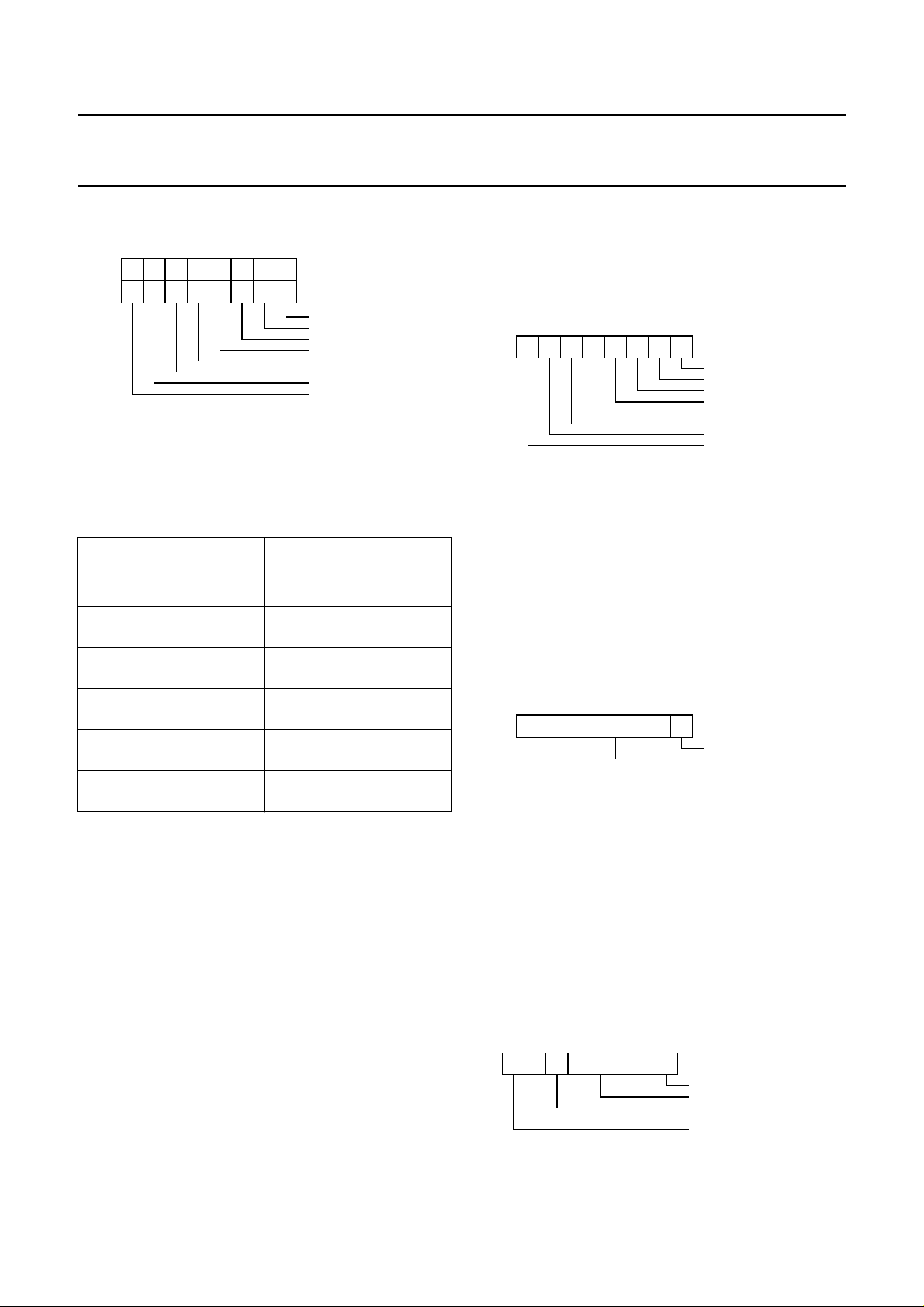
ET MODE
1999 May 10 31
Command: F3h.
Data: write 1 byte.
Page 32
Philips Semiconductors Preliminary specification
Universal Serial Bus (USB) CODEC UDA1325
An interrupt is also generated after a bus reset. When the
76543210
Reset value
11111100
T T F F T T T T
Bus Reset
IsoOut
IsoIn
IntIsoOut
IntIsoIn
ErrorDebugMode
AlwaysPLLClock
Reserved
Reserved
Reset value: gives the value of the bits after Power-on
reset. Bus reset: a ‘F’ indicates that the value of the bit is
not changed during a bus reset. a ‘T’ indicates that during
a bus reset, the bit is reset to its reset value.
interrupt register consists of all zeros, and an interrupt was
generated, there was a bus reset. The interrupt is cleared
when the interrupt register is read.
76543210
0 0 0 0 0 0 0 0
ELECT ENDPOINT
S
Power On Value
Control OUT
Control IN
Endpoint 1 OUT
Endpoint 1 IN
Endpoint 2 IN
Endpoint 3 IN
Endpoint 4 OUT
Endpoint 5 IN
Table 25
BIT DESCRIPTION
IsoOut ISO out endpoint can be
used
IsoIn ISO in endpoint can be
used
IntIsoOut allow interrupt from ISO
out endpoint
IntIsoIn allow interrupt from ISO in
endpoint
ErrorDebugMode Setting chip in debug
mode
AlwaysPLLClock the PLL clock must keep
on running
Data flow commands
Data flow commands are used to manage the data
transmission between the USB endpoints and the host.
Much of the data flow is initiated via the interrupt to the
microcontroller. The microcontroller uses these
commands to access the endpoint buffers and determine
whether the endpoint buffers have valid data.
R
EAD INTERRUPT REGISTER
Command: F4h.
Data: read 1 byte.
The read interrupt register command returns the value of
the interrupt register. Every time a packet is received or
transmitted, an interrupt will be generated and a flag
specific to the physical endpoint will be set in the interrupt
register. Reading the status of the endpoint will clear the
flag.
Command: 00h + endpoint index.
Data: optional read 1 byte.
The select endpoint command initializes an internal
pointer to the start of the selected buffer. Optionally, this
command can be followed by a data read. Bit 0 is low if the
buffer is empty and high if the buffer is full. There is one
command for every endpoint.
76543210
XXXXXXX0
ET ENDPOINT STATUS
G
Power On Value
Full/Empty
Reserved
Command: 40h + endpoint index.
Data: read 1 byte.
The get endpoint status command is followed by one data
read that returns the status of the last transaction of the
selected endpoint. This command also resets the
corresponding interrupt flag in the interrupt register, and
clears the status, indicating that it was read. There is one
command for every endpoint.
76543210
0 0 00 0
000
Power On Value
Data Receive/Transmit
Error Code
Setup Packet
Data 0/1 Packet
Previous Status not Read
1999 May 10 32
Page 33
Philips Semiconductors Preliminary specification
Universal Serial Bus (USB) CODEC UDA1325
Table 26 Error codes
ERROR
CODE
RESULT
0000 no error
0001 PID encoding error; bits 7 to 4 in the PID
token are not the inversion of bits 3 to 0
0010 PID unknown; PID encoding is valid, but PID
does not exist
0011 unexpected packet; packet is not of the type
expected (token, data or acknowledge), or
SETUP token received on non-control
endpoint
0100 token CRC error
0101 data CRC error
0110 time out error
0111 babble error
1000 unexpected end-of-packet
1001 sent or received NAK
1010 sent stall, a token was received, but the
endpoint was stalled
1011 overflow error, the received data packet was
larger then the buffer size of the selected
endpoint
1100 sent empty packet (ISO only)
1101 bitstuff error
1110 error in sync
1111 wrong data PID
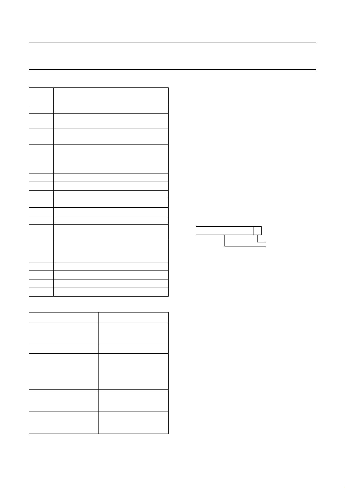
Table 27
BIT DESCRIPTION
Data receive/transmit a ‘1’ indicates data has
been received or
transmitted successfully
Error code see Table 26
Setup packet a ‘1’ indicates the last
received packet had a
SETUP token (this will
always read ‘0’ for IN
buffers)
Data 0/1 packet a ‘1’ indicates the last
received packet had a
DATA 1 PID
Previous status not read a ‘1’ indicates a second
event occurred before the
previous status was read
SET ENDPOINT STATUS
Command: 40h + endpoint index.
Data: write 1 byte.
This command is used to stall or unstall an endpoint. Only
the least significant bit has a meaning. When the stalled bit
is equal to 1, the endpoint is stalled, when equal to 0, the
endpoint is unstalled. There is one command for every
endpoint.
A stalled control endpoint is automatically unstalled when
it receives a SETUP token, regardless of the contents of
the packet. If the endpoint should stay in stalled state, the
microcontroller should restall it.
When a stalled endpoint is unstalled, it is also re-initialized.
This means that its buffer is flushed and the next DATA
PID that will be sent or expected (depending on the
direction of the endpoint) is DATA0.
01234567
0
Power On Value
Stalled
Reserved
EAD BUFFER
R
X
XXX XXX
Command: F0h.
Data: read n bytes (max. 10).
The read buffer command is followed by a number of data
reads, which returns the contents of the selected endpoint
data buffer. After each read, the internal buffer pointer is
incremented by 1.
The buffer pointer is not reset to the buffer start by the read
buffer command. This means that reading a buffer can be
interrupted by any other command (except for select
endpoint).
1999 May 10 33
Page 34

Philips Semiconductors Preliminary specification
Universal Serial Bus (USB) CODEC UDA1325
The data in the buffer are organized as follows:
Byte 0: transfer successful, number of data bytes (MSB)
Byte 1: number of data bytes (LSB)
Byte 2: data byte 0
Byte 3: data byte 1
Byte 4: data byte 2
Byte 5: data byte 3
Byte 6: data byte 4
Byte 7: data byte 5
Byte 8: data byte 6
Byte 9: data byte 7.
Bytes 0 and 1 indicate the number of bytes in the buffer.
Byte 0 is the Most Significant Byte (MSB). Byte 1 is the
Least Significant Byte (LSB). Only bits 1 and 0 of byte 0
are used in the number of bytes indication.
Bit 7 of byte 0 indicates if the transaction was successful
(bit 7 is ‘1’ if the transaction was successful). Bits 6 to 2 of
byte 0 are reserved.
RITE BUFFER
W
Command: F0h.
Data: write n bytes (max. 10).
The write buffer command is followed by a number of data
writes, which load the endpoint buffer. After each write, the
internal buffer pointer is incremented by 1.
acknowledged explicitly that it has seen the SETUP
packet.
If the microcontroller is reading the data from a SETUP
packet, and a new SETUP packet arrives, the device must
accept this new SETUP packet. So the data, currently
being read by the microcontroller, is overwritten with the
new packet. On the arrival of the new packet, the
commands validate buffer and clear buffer are disabled.
If the microcontroller has finished reading the data from
the buffer, it will try to clear the buffer. The device will
ignore this command, so the new SETUP packet in the
buffer is not cleared. The microcontroller will now detect
the interrupt of the new SETUP packet and will start
reading the new data in the buffer.
A SETUP token can be followed by an IN token. After the
SETUP token, the microcontroller will start filling the IN
buffer. A SETUP token will clear the IN buffer. This avoids
the following problem: after a SETUP token, the
microcontroller fills the IN buffer. If the SETUP token is
followed by a SETUP token and shortly followed by an IN
token, the device will send the contents of the IN buffer to
the host. The IN buffer was filled after the first SETUP
token. That is why after a SETUP token the IN buffer is
cleared.
If the microcontroller is still filling the buffer when the
second SETUP token arrives, the SETUP token will clear
the IN buffer. If the microcontroller has filled the IN buffer,
it will validate the buffer. So clearing the IN buffer on
receiving a SETUP token is not enough.
The buffer pointer is not reset to the buffer start by the write
buffer command. This means that writing a buffer can be
interrupted by any other command (except for select
endpoint).
The data must be organized in the same way as described
in the read buffer command. Bits 7 to 2 of byte 0 are
reserved and must be filled with zeros.
CKNOWLEDGE SETUP
A
Command: F1h.
Data: none.
The arrival of a SETUP packet flushes the IN buffer and
disables the validate buffer and clear buffer commands for
both IN and OUT endpoints.
The microcontroller needs to re-enable these commands
by the acknowledge setup command. This ensures that
the last SETUP packet stays in the buffer and no packet
can be sent back to the host until the microcontroller has
1999 May 10 34
If a SETUP token is received, the device will also disable
the validate buffer command for the IN buffer. If the
microcontroller needs to fill the buffer after a SETUP token,
the command acknowledge setup command must be sent
to enable the validate buffer command.
C
LEAR BUFFER
Command: F2h.
Data: none.
When a packet is received completely, an internal
endpoint buffer full flag is set. All subsequent packets will
be refused by returning a NACK to the host. When the
microcontroller has read the data, it should free the buffer
by the clear buffer command. When the buffer is cleared,
new packets will be accepted.
Page 35
Philips Semiconductors Preliminary specification
Universal Serial Bus (USB) CODEC UDA1325
VALIDATE BUFFER
Command: FAh.
Data: none.
When the microcontroller has written data into an IN buffer,
it should set the buffer full flag by the validate buffer
command. This indicates that the data in the buffer are
valid and can be sent to the host when the next IN token is
received.
General commands
READ CURRENT FRAME NUMBER
Command: F5h.
Data: read 1 or 2 bytes.
This command is followed by one or two data reads and
returns the frame number of the last successfully received
SOF. The frame number is eleven bits wide. The frame
number is returned least significant byte first. In case the
user is only interested in the lower 8 bits of the frame
number only the first byte needs to be read.
2
C MASTER/SLAVE INTERFACE
I
The I2C module implements a master/slave I2C-bus
interface with integrated shift register, shift timing
generation and slave address recognition. It is compliant
to the I2C-bus specification IC20/Jan92. I2C standard
mode (100 kHz SCL) and fast mode (400 kHz) are
supported. Low speed mode and extended 10 bit
addressing are unsupported.
2
Characteristics of the I
C-bus
The I2C-bus is for 2-way, 2-line communication between
different ICs or modules. The two lines are a serial data
line (SDA) and a Serial Clock Line (SCL). Both lines must
be connected to V
via a pull-up resistor.
DDE
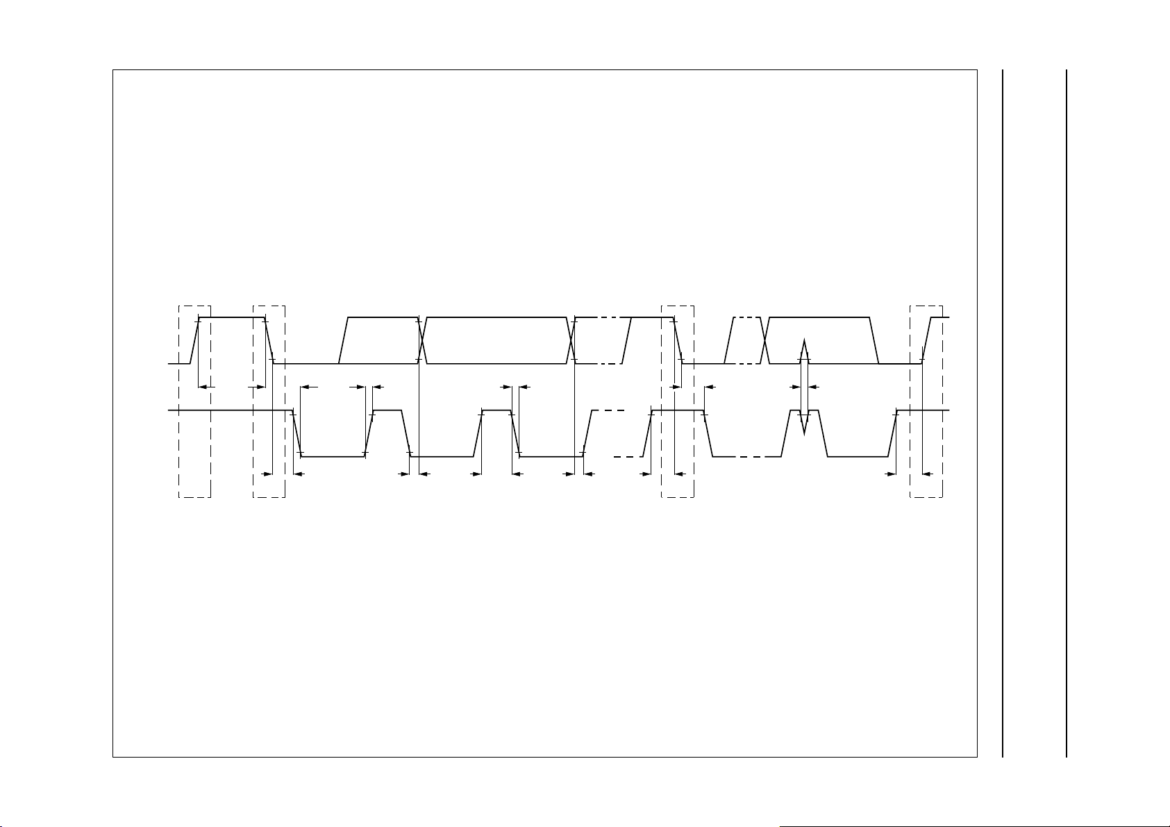
The timing definition of the I2C-bus is given in Fig.7.
Programmer’s view
For a detailed description of the I
2
C-bus protocol refer to
Philips Integrated Circuits Data Handbook IC20, 8XC552.
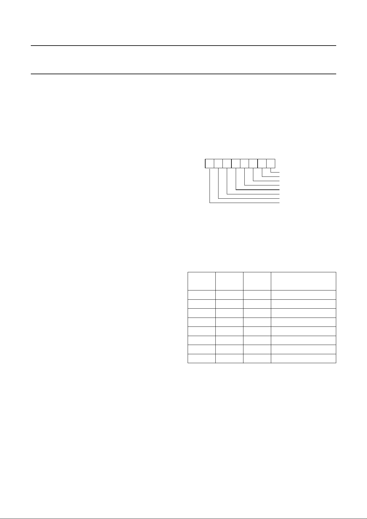
S1CON register
The CPU can read from and write to this 8-bit SFR.
Two bits are effected by the SIO1 hardware: the SI bit is
set when a serial interrupt is requested, and the STO bit is
cleared when a STOP condition is present on the I
2
C-bus.
The STO bit is also cleared when ENS1 = ‘0’. Reset
initializes S1CON to 00h.
76543210
Power On Value
CR0
CR1
AA
SI
STO
STA
ENS1
CR2
CR2, 1
0 0 0 0 0 0 0 0
AND 0-THE CLOCK RATE BITS
These three bits determine the serial clock frequency
when SIO1 is in a master mode.
The various serial rates are shown in Table 28.
Table 28 Serial clock rates (SCL line)
2
I
CR2 CR1 CR0
C BIT FREQUENCY
(kHz)
0 0 0 1200
0 0 1 600
0 1 0 400
0 1 1 300
1 0 0 150
1 0 1 100
110 75
1 1 1 3.9 ... 501
When the CR bits are ‘111’, the maximum bit rate for the
data transfer will be derived from the Timer 1 overflow rate
divided by 2 (i.e. every time the Timer 1 overflows, the
SCL signal will toggle).
The programmer’s view of the I2C library function is -with
one exception- identical to that of the 8XC552
microcontroller. Only the bit rate frequency selection in
S1CON and the handling of the Timer 1 overflow
information deviates to accommodate 400 kHz operation.
1999 May 10 35
Page 36
This text is here in white to force landscape pages to be rotated correctly when browsing through the pdf in the Acrobat reader.This text is here in
_white to force landscape pages to be rotated correctly when browsing through the pdf in the Acrobat reader.This text is here inThis text is here in
white to force landscape pages to be rotated correctly when browsing through the pdf in the Acrobat reader. white to force landscape pages to be ...
1999 May 10 36
SDA
Philips Semiconductors Preliminary specification
Universal Serial Bus (USB) CODEC UDA1325
SCL
t
BUF
P
S
t
LOW
t
HD;STA
t
r
t
HD;DAT
t
HIGH
t
f
t
SU;DAT
t
SU;STA
Sr
t
HD;STA
t
SP
t
SU;STO
MBC611
P
Fig.7 Definition of timing of the I2C-bus.
handbook, full pagewidth
Page 37
Philips Semiconductors Preliminary specification
Universal Serial Bus (USB) CODEC UDA1325
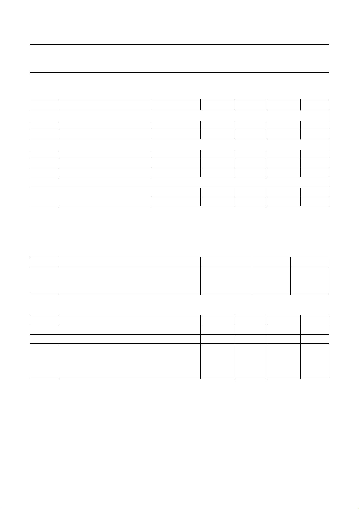
LIMITING VALUES
In accordance with the Absolute Maximum Rating System (IEC 134).
SYMBOL PARAMETER CONDITIONS MIN. TYP. MAX. UNIT
All digital I/Os
V
I/O
I
O
DC input/output voltage range −0.5 − V
output current V
Temperature values
T
j
T
stg
T
amb
junction temperature 0 − 125 °C
storage temperature −55 − +150 °C
operating ambient temperature 0 25 70 °C
Electrostatic handling
V
es
electrostatic handling note 1 −3000 − +3000 V
DDE
= 5.0 V −−4mA
DDE
note 2 −300 − +300 V
V
Notes
1. Equivalent to discharging a 100 pF capacitor through a 1.5 kΩ series resistor.
2. Equivalent to discharging a 200 pF capacitor through a 2.5 µH series conductor.
THERMAL CHARACTERISTICS
SYMBOL PARAMETER CONDITIONS VALUE UNIT
R
th(j-a)
thermal resistance from junction to ambient
UDA1325PS in free air 48 K/W
UDA1325H in free air 48 K/W
RECOMMENDED OPERATING CONDITIONS
SYMBOL PARAMETER MIN. TYP. MAX. UNIT
V
V
V
DDE
DD
I
supply voltage periphery (I/O) 4.75 5.0 5.25 V
supply voltage (core) 3.0 3.3 3.6 V
DC input voltage range
for D+ and D− 0.0 − V
for VINL and VINR − 0.5V
DD
for digital I/Os 0.0 − V
DD
− V
DDE
V
V
1999 May 10 37
Page 38
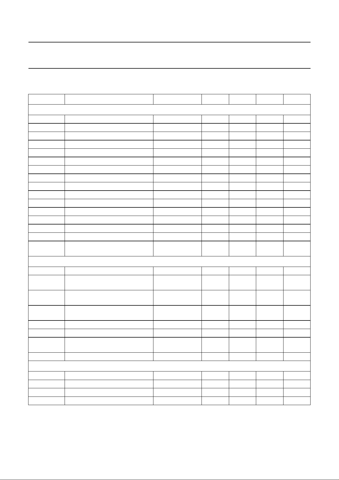
Philips Semiconductors Preliminary specification
Universal Serial Bus (USB) CODEC UDA1325
DC CHARACTERISTICS
= 5.0 V; VDD= 3.3 V; T
V
DDE
SYMBOL PARAMETER CONDITIONS MIN. TYP. MAX. UNIT
Supplies
V
DDE
V
DDI
V
DDA1
V
DDA2
V
DDA3
V
DDO
V
DDX
I
DDE
I
DDI
I
DDA1
I
DDA2
I
DDA3
I
DDO
I
DDX
P
tot
P
ps
digital supply voltage periphery 4.75 5.0 5.25 V
digital supply voltage core 3.0 3.3 3.6 V
analog supply voltage 1 3.0 3.3 3.6 V
analog supply voltage 2 3.0 3.3 3.6 V
analog supply voltage 3 3.0 3.3 3.6 V
operational amplifier supply voltage 3.0 3.3 3.6 V
crystal oscillator supply voltage 3.0 3.3 3.6 V
digital supply current periphery note 1 − 3.7 − mA
digital supply current core − 39.0 − mA
analog supply current 1 − 3.6 − mA
analog supply current 2 − 8.0 − mA
analog supply current 3 − 0.9 9.0
operational amplifier supply current − 3.0 − mA
crystal oscillator supply current − 1.2 13.0
total power dissipation − 200 − mW
total power dissipation in power
saving mode
=25°C; f
amb
= 48 MHz; fs= 44.1 kHz; unless otherwise specified.
osc
note 4 − 1.2 − mW
(2)
(3)
mA
mA
Inputs/outputs D+ and D−
V
V
I
O(H)
static DC input voltage −0.5 − V
static DC output voltage HIGH RL=15kΩ
2.8 − 3.6 V
DDI
V
connected to GND
V
O(L)
high impedance data line output
I
LO
static DC output voltage LOW RL= 1.5 kΩ
connected to V
−−0.3 V
DD
−−10 µA
leakage current
V
I(diff)
V
CM(diff)
V
SE(R)(th)
differential input sensitivity 0.2 −−V
differential common mode range 0.8 − 2.5 V
single-ended receiver threshold
0.8 − 2.0 V
voltage
C
IN
transceiver input capacitance pin to GND −−20 pF
Digital input pins
V
IL
V
IH
input leakage current −−1µA
I
LI
C
I
LOW-level input voltage −−0.3V
HIGH-level input voltage 0.7V
DDE
− V
DDE
DDE
V
V
input capacitance −−5pF
1999 May 10 38
Page 39

Philips Semiconductors Preliminary specification
Universal Serial Bus (USB) CODEC UDA1325
SYMBOL PARAMETER CONDITIONS MIN. TYP. MAX. UNIT
PGA and ADC
V
ref(AD)
V
ref(ADC)(pos)
V
ref(ADC)(neg)
V
I(PGA)
R
I(PGA)
Filter stream DAC
V
ref(DA)
V
O(CM)
R
O(VOUT)
R
O(L)
C
O(L)
Notes
1. This value depends strongly on the application. The specified value is the typical value obtained using the application
diagram as illustrated in Fig.8.
2. At start-up of the OSCAD oscillator.
3. At start-up of the OSC48 oscillator.
4. Exclusive the IDDE current which depends on the components connected to the I/O pins.
reference voltage PGA and ADC − 0.5V
positive reference voltage of the
− V
DDA2
DDA2
− V
− V
ADC
negative reference voltage of the
− 0.0 − V
ADC
DC input voltage VINL and VINR of
− 0.5V
DDA2
− V
the PGA
DC input resistance at VINL and
− 12.5 − kΩ
VINR of the PGA
reference voltage DAC − 0.5V
common mode output voltage − 0.5V
output resistance at VOUTL and
− 11 −Ω
DDA1
DDA1
− V
− V
VOUTR
output load resistance 2.0 −−kΩ
output load capacitance −−50 pF
1999 May 10 39
Page 40
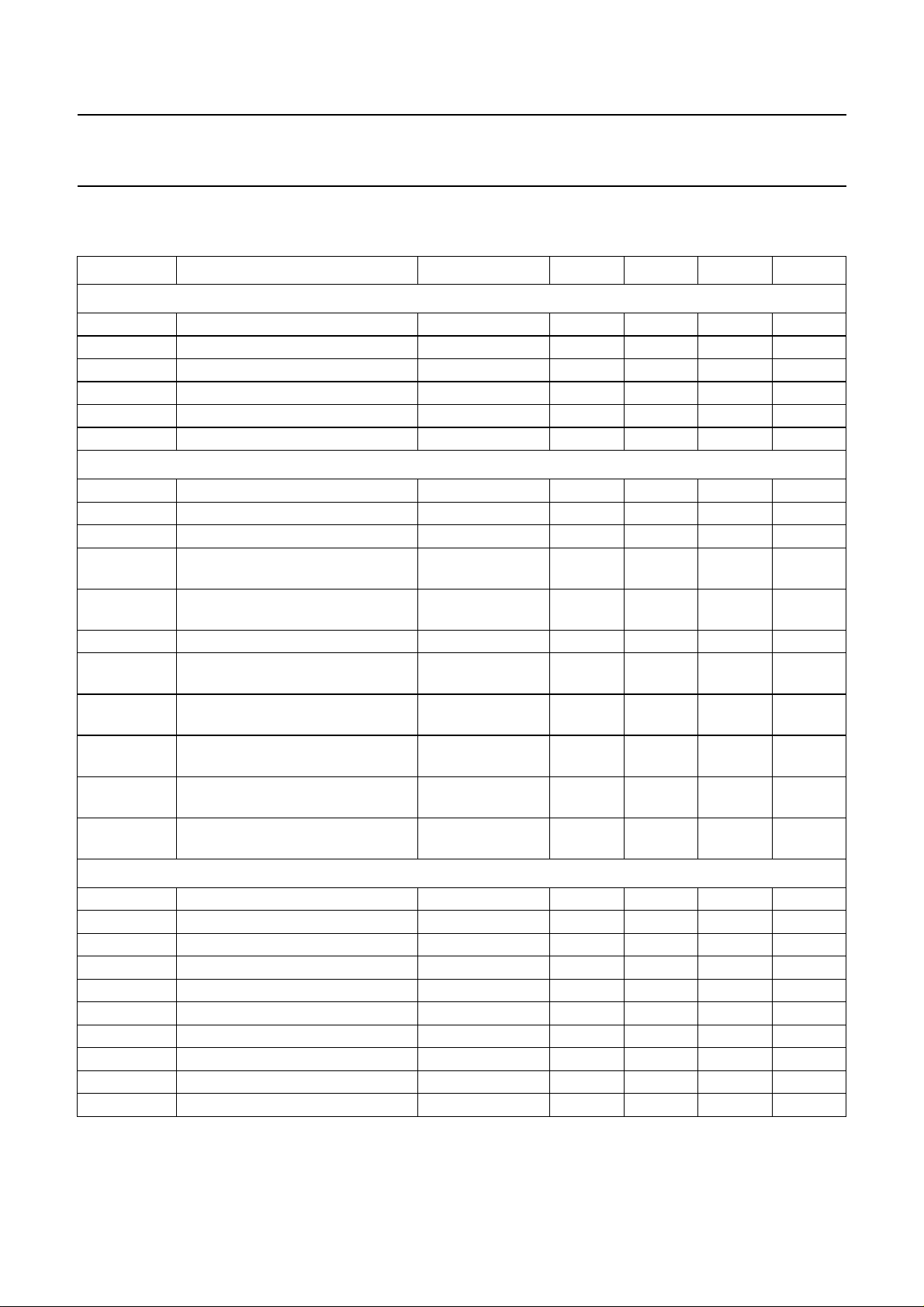
Philips Semiconductors Preliminary specification
Universal Serial Bus (USB) CODEC UDA1325
AC CHARACTERISTICS
= 5.0 V; V
V
DDE
SYMBOL PARAMETER CONDITIONS MIN. TYP. MAX. UNIT
Driver characteristics D+ and D− (full-speed mode)
f
o(s)
t
r
t
f
t
rf(m)
V
cr
R
o(drive)
Data source timings D+ and D− (full-speed mode)
f
i(s)
f
fs(D)
t
fr(D)
t
J1(diff)
t
J2(diff)
t
W(EOP)
t
EOP(diff)
t
JR1
t
JR2
t
EOPR1
t
EOPR2
= 3.3 V; T
DDI
amb
=25°C; f
= 48 MHz; fs= 44.1 kHz; unless otherwise specified.
osc
audio sample output frequency 5 − 55 kHz
rise time CL=50pF 4 − 20 ns
fall time CL=50pF 4 − 20 ns
rise/fall time matching (tr/tf)90−110 %
output signal crossover voltage 1.3 − 2.0 V
driver output resistance steady-state drive 28 − 43 Ω
audio sample input frequency 5 − 55 kHz
full speed data rate 11.97 12.00 12.03 Mbits/s
frame interval 0.9995 1.0000 1.0005 ms
source differential jitter to next
−3.5 0.0 +3.5 ns
transition
source differential jitter for paired
−4.0 0.0 +4.0 ns
transitions
source end of packet width 160 − 175 ns
differential to end of packet
−2.0 − +5.0 ns
transition skew
receiver data jitter tolerance to next
−18.5 0.0 +18.5 ns
transition
receiver data jitter tolerance for
−9.0 0.0 +9.0 ns
paired transitions
end of packet width at receiver
40 −−ns
must reject as end of packet
end of packet width at receiver
82 −−ns
must accept as end of packet
Serial input/output data timing
f
s
f
i(WS)
t
r
t
f
t
BCK(H)
t
BCK(L)
t
s;DAT
t
h;DAT
t
s;WS
t
h;WS
system clock frequency − 12 − MHz
word selection input frequency 5 − 55 kHz
rise time −−20 ns
fall time −−20 ns
bit clock HIGH time 55 −−ns
bit clock LOW time 55 −−ns
data set-up time 10 −−ns
data hold time 20 −−ns
word selection set-up time 20 −−ns
word selection hold time 10 −−ns
1999 May 10 40
Page 41
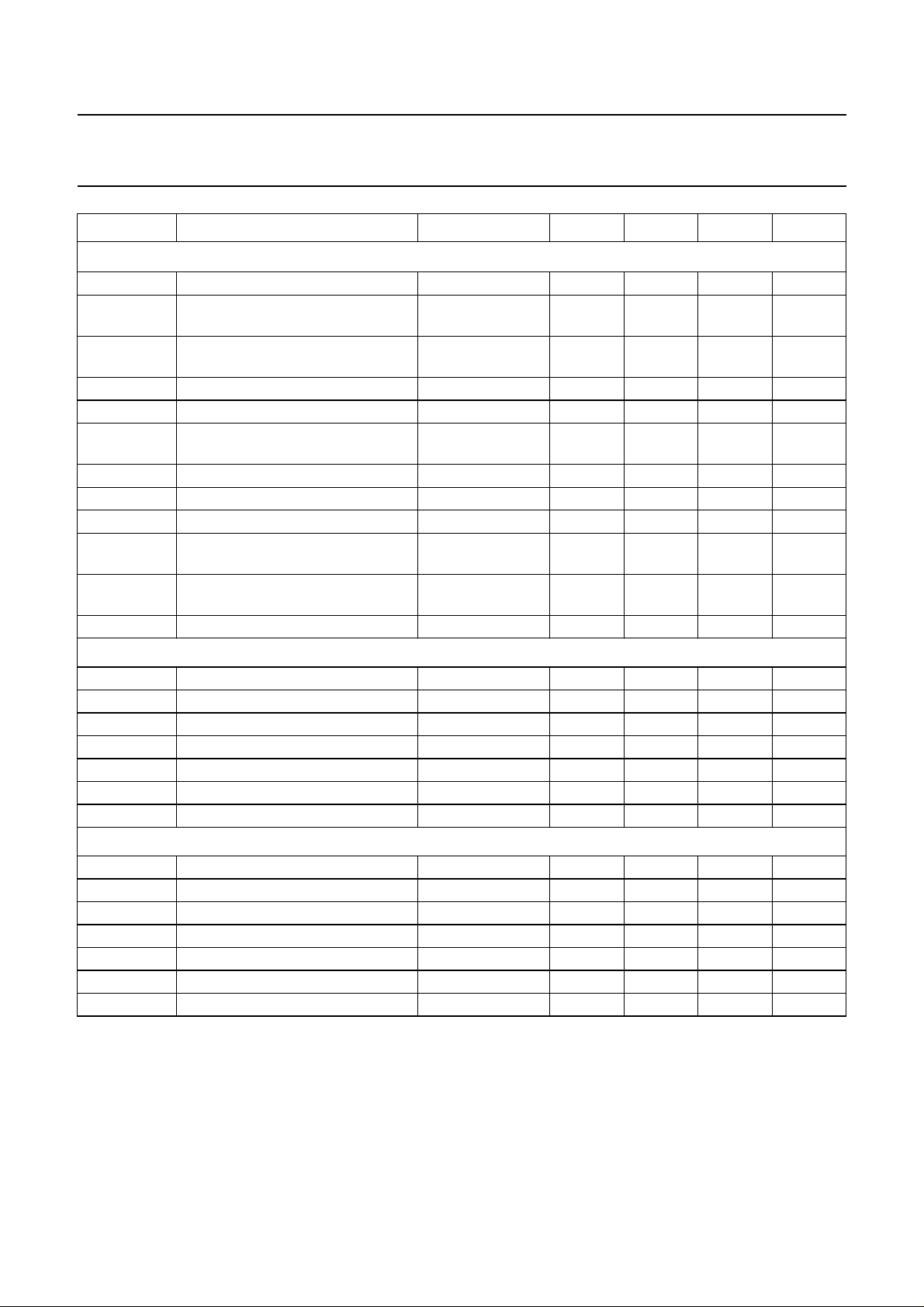
Philips Semiconductors Preliminary specification
Universal Serial Bus (USB) CODEC UDA1325
SYMBOL PARAMETER CONDITIONS MIN. TYP. MAX. UNIT
SDA and SCL lines for 100 kHz I2C devices
f
SCL
t
BUF
t
HD;STA
t
LOW
t
HIGH
t
SU;STA
t
SU;STO
t
HD;DAT
t
SU;DAT
t
r
t
f
C
L(bus)
Oscillator 1 (system clock)
f
osc
δ duty factor − 50 − %
g
m
R
o
C
i(XTAL1a)
C
i(XTAL2a)
I
start
Oscillator 2 (for ADC clock)
f
osc
δ duty cycle − 50 − %
g
m
R
o
C
i(XTAL1b)
C
i(XTAL2b)
I
start
SCL clock frequency 0 − 100 kHz
bus free time between a STOP and
4.7 −−µs
START condition
hold time (repeated) START
4.0 −−µs
condition
LOW period of the SCL clock 4.7 −−µs
HIGH period of the SCL clock 4.0 −−µs
set-up time for a repeated START
4.7 −−µs
condition
set-up time for STOP condition 4.0 −−µs
data hold time 5.0 −−µs
data set-up time 250 −−ns
rise time of both SDA and SCL
−−1000 ns
signals
fall time of both SDA and SCL
−−300 ns
signals
capacitive load for each bus line −−400 pF
oscillator frequency − 48 − MHz
transconductance 12.8 22.1 30.2 mS
output resistance 0.6 1.1 2.3 kΩ
parasitic input capacitance XTAL1a 4.5 4.8 5.2 pF
parasitic input capacitance XTAL2a 4.1 4.6 5.0 pF
start-up current 3.7 7.6 13.0 mA
oscillator frequency 8.192 − 14.08 MHz
transconductance 8.1 13.6 18.1 mA/V
output resistance 1.3 2.0 4.0 kΩ
parasitic input capacitance XTAL1b 5.0 5.4 5.7 pF
parasitic input capacitance XTAL2b 4.1 4.6 5.0 pF
start-up current 2.4 5.0 8.4 mA
1999 May 10 41
Page 42

Philips Semiconductors Preliminary specification
Universal Serial Bus (USB) CODEC UDA1325
SYMBOL PARAMETER CONDITIONS MIN. TYP. MAX. UNIT
Analog PLL (for ADC clock)
f
clk(PLL)
δ duty factor − 50 − %
t
strt(PO)
Power-on reset
t
su(PO)
PGA and ADC
V
i(FS)(rms)
C
i(PGA)
(THD + N)/S total harmonic distortion plus
S/N signal to noise ratio Vi= 0.0 V 90 95 − dBA
α
ct
f
s
OL digital output level PGA gain=0dB,
PLL clock frequency 8.1920 11.2896 12.2880 MHz
start-up time after power-on −−10 ms
power-on set-up-time note 1 25C
full-scale input voltage (RMS value) PGA gain = −3dB − 1414
ref
(2)
−−ms
(3)
− mV
PGA gain=0dB − 1000 − mV
PGA gain=3dB − 708 − mV
PGA gain=9dB − 355 − mV
PGA gain = 15 dB − 178 − mV
PGA gain = 21 dB − 89 − mV
PGA gain = 27 dB − 44 − mV
input capacitance of the PGA −−20 pF
f
= 44.1 kHz at
s
noise-to-signal ratio
input signal of
1 kHz; PGA
gain = 0 dB;
note 4
V
(0 dB)
i
1.0 V (RMS)
V
(−60 dB) −−30 −20 dB
i
−−85 −80 dB
− 0.0056 0.01 %
− 3.2 10.0 %
crosstalk between channels PGA gain=0dB − 100 − dB
sample frequency (128fs) 0.640 − 7.04 MHz
−−2.0 − dBFS
V
= 1 V (RMS)
i
1999 May 10 42
Page 43

Philips Semiconductors Preliminary specification
Universal Serial Bus (USB) CODEC UDA1325
SYMBOL PARAMETER CONDITIONS MIN. TYP. MAX. UNIT
Filter stream DAC
RES resolution 16 −−bits
V
o(FS)(rms)
SVRR supply voltage ripple rejection at
∆V
channel unbalance maximum volume − 0.03 − dB
o
α
ct
(THD + N)/S total harmonic distortion plus
S/N signal-to-noise ratio at bipolar zero A-weighting at
full-scale output voltage
VDD= 3.3 V − 0.66 − V
(RMS value)
f
V
DDA
and V
DDO
ripple
V
ripple(p-p)
= 1 kHz
= 0.1 V
− 60 − dB
crosstalk between channels RL=5kΩ−95 − dB
f
= 44.1 kHz;
s
noise-to-signal ratio
RL=5kΩ; note 5
at input signal of
1 kHz (0 dB)
at input signal of
1 kHz (−60 dB)
−−90 −80 dB
− 0.0032 0.01 %
−−30 −20 dB
− 3.2 10 %
90 95 − dB
code 0000H
Notes
1. Strongly depends on the external decoupling capacitor connected to V
2. C
in µF.
ref
ref(DA)
.
3. Although a level of 1.414 V (RMS) would be required to optimal drive the ADC in this gain setting, this level can not
be used. Due to the 3.3 V supply voltage input, signals of 1.17 V (RMS) and higher will result in clipping.
4. Measured with the APLL as ADC clock source.
5. Measured with I2S-bus input as digital source.
1999 May 10 43
Page 44
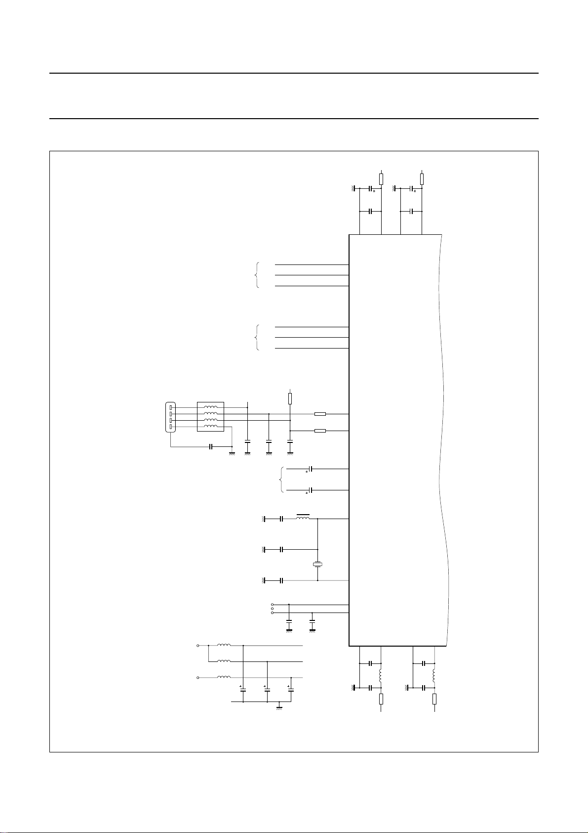
Philips Semiconductors Preliminary specification
Universal Serial Bus (USB) CODEC UDA1325
APPLICATION INFORMATION
handbook, full pagewidth
X4
1
1
2
2
3
3
45
4
C15
10 nF
(50 V)
+V
A
R35
1 Ω
C34
47 µF
(16 V)
C38
100 nF
(63 V)
V
V
DDA1
SSA1
3839
GP0/BCKI
BCKI
digital
input
WSI
playback
recording
L1
8
7
6
digital
input
DI
BCK
WS
DA
+V
C
C18
22 pF
(63 V)
C44
10 nF (63 V)
R48
1.5 kΩ
C17
22 pF
(63 V)
C8
47 µF (16 V)
C22
47 µF (16 V)
L5
1.5 µH
22 Ω
R16
22 Ω
R7
V
USB
C16
10 nF
(50 V)
analog
input
recording
GP5/WSI
1
GP1/DI
BCK
VINR
VINL
XTAL2b
17
15
13
61
WS
59
DA
57
D−
6
D+
8
47
43
26
UDA1325H
C32
47 µF
(16 V)
C21
100 nF
(63 V)
V
SSA2
+V
A
R27
1 Ω
V
DDA2
4244
C38
12 pF (63 V)
C37
12 pF (63 V)
ADC XTAL
V
V
A(ext)
D(ext)
L8
BLM32A07
L7
BLM32A07
L6
BLM32A07
GND
C47
100 µF
(16 V)
C46
100 µF
(16 V)
Fig.8 Application diagram UDA1325H (continued in Fig.9).
1999 May 10 44
C5
18 pF
(50 V)
C45
100 µF
(16 V)
+V
+V
+V
X1 48 MHz
XTAL1b
XTAL2a
XTAL1a
C6
18 pF
(50 V)
A
C
D
MGM760
25
53
54
10
V
SSI
C25
100 nF
(63 V)
C24
100 nF
(63 V)
9
V
DDI
L2
BLM32A07
R17
1 Ω
+V
C
11
V
SSE
100 nF
(63 V)
100 nF
(63 V)
C26
C27
12
V
DDE
L3
BLM32A07
R25
1 Ω
+V
D
Page 45
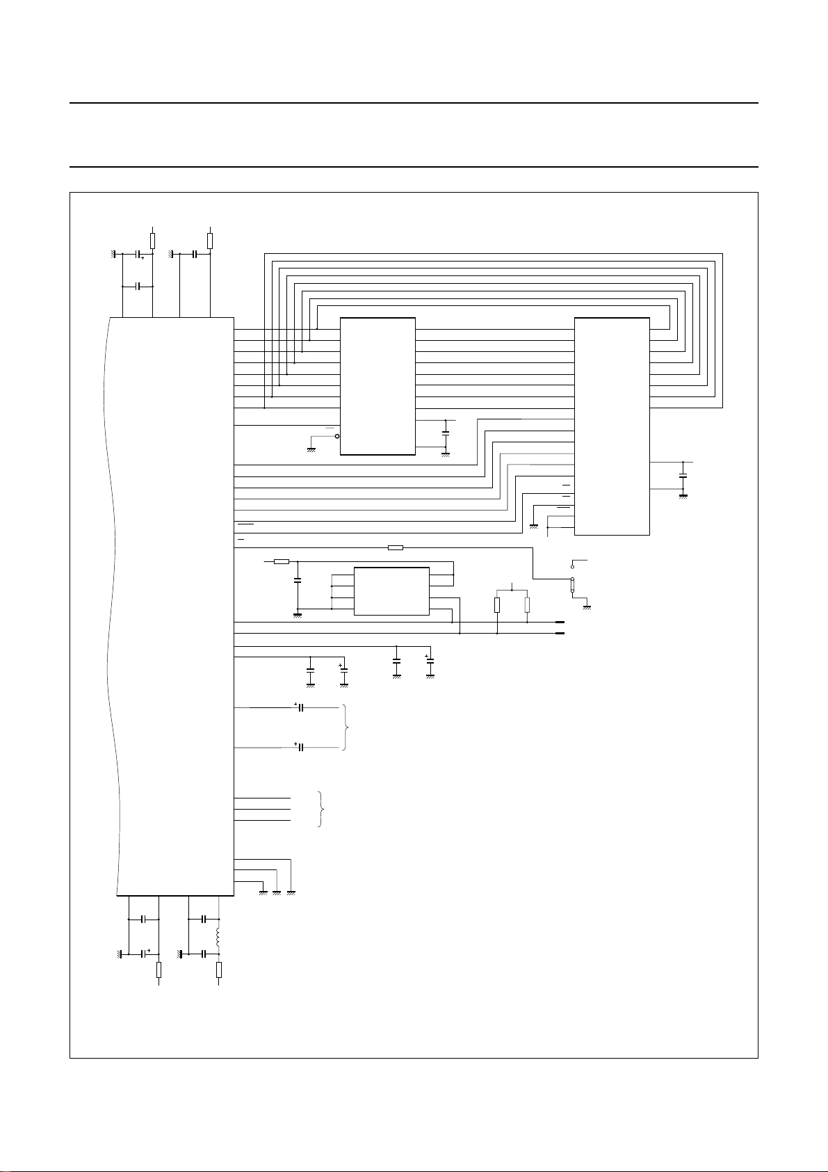
Philips Semiconductors Preliminary specification
Universal Serial Bus (USB) CODEC UDA1325
handbook, full pagewidth
C7
47 µF
(16 V)
C19
100 nF
(63 V)
V
V
SSA3
5255
UDA1325H
+V
R10
1 Ω
A
DDA3
C11
100 nF
(63 V)
+V
A
R8
1 Ω
VRPVRN
5149
P0.0
56
P0.1
58
P0.2
60
P0.3
62
P0.4
64
P0.5
3
P0.6
5
P0.7
7
ALE
50
P2.0
14
P2.1
16
P2.2
18
P2.3
20
P2.4
22
P2.5
23
PSEN
31
EA
48
21
19
40
41
37
34
+V
SDA
SCL
V
ref(DA)
V
ref(AD)
VOUTR
VOUTL
R20
D
1 Ω
47 µF (16 V)
47 µF (16 V)
C35
C48
C36
100 nF
(63 V)
C28
100 nF
(63 V)
D
7
18
D
6
17
D
5
14
D
4
13
D
3
8
2
1
0
V
74HCT373D
7
4
3
11
1
A0
1
A1
2
A2
3
SS
4
C31
47 µF
(16 V)
analog
output
playback
D1
PCF85116-3
D
D
D
LE
OE
R28
4.7 kΩ
D4
19
16
15
12
9
6
5
2
20
10
C29
100 nF
(63 V)
Q
Q
Q
Q
Q
Q
Q
Q
V
GND
8
7
6
5
R39
10 kΩ
A0
10
A1
9
A2
8
A3
7
A4
6
A5
5
A6
4
A7
3
A8
A9
A10
A11
A12
A13
OE
CE
PGM
V
PP
+V
D
J3
1
2
25
24
21
23
2
26
22
20
27
1
3
2
1
2
(I
C-bus)
D2
EEPM27128
+V
D
(internal ROM)
(external ROM)
7
6
5
4
3
2
1
0
CC
+V
D
100 nF
C24
(50 V)
V
PTC
SCL
SDA
DD
C41
47 µF
(16 V)
+V
R38
10 kΩ
D
O0
11
O1
12
O2
13
O3
15
O4
16
O5
17
O6
18
O7
19
V
CC
C25
+V
100 nF
(50 V)
D
28
GND
14
GP4/BCKO
33
V
SSO
C33
100 nF
(63 V)
C39
47 µF
(16 V)
2
GP3/WSO
1
GP2/DO
63
RTCB
36
TC
35
SHTCB
4
24
V
SSX
100 nF
(63 V)
100 nF
(63 V)
C28
C18
28
V
DDX
L13
BLM32A07
R26
1 Ω
+V
C
32
V
DDO
R43
1 Ω
+V
A
MGM761
BCKO
WSO
DO
digital
output
playback
Fig.9 Application diagram UDA1325H (continued from Fig.8).
1999 May 10 45
Page 46
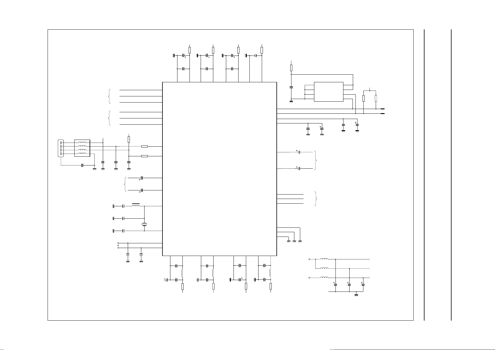
This text is here in white to force landscape pages to be rotated correctly when browsing through the pdf in the Acrobat reader.This text is here in
d
_white to force landscape pages to be rotated correctly when browsing through the pdf in the Acrobat reader.This text is here inThis text is here in
white to force landscape pages to be rotated correctly when browsing through the pdf in the Acrobat reader. white to force landscape pages to be ...
1999 May 10 46
X4
L1
1
1
2
2
3
3
45
4
C15
10 nF
(50 V)
8
7
6
digital
input
playback
digital
input
recording
V
USB
C16
10 nF
(50 V)
ADC XTAL
BCKI
WSI
DI
BCK
WS
DA
analog
input
recording
10 nF (63 V)
12 pF (63 V)
12 pF (63 V)
C18
22 pF
(63 V)
C44
C38
C37
+V
C
R48
1.5 kΩ
C17
22 pF
(63 V)
1.5 µH
C5
18 pF
(50 V)
L5
47 µF (16 V)
47 µF (16 V)
GP0/BCKI
GP5/WSI
R7
22 Ω
R16
22 Ω
C8
C22
1
XTAL2b
X1 48 MHz
XTAL1b
XTAL2a
XTAL1a
C6
18 pF
(50 V)
GP1/DI
BCK
VINR
VINL
+V
A
R35
1 Ω
C34
47 µF
(16 V)
C38
100 nF
(63 V)
V
SSA1
16
15
14
3
WS
2
DA
1
D−
8
D+
9
36
34
21
20
40
41
11
10
V
V
DDI
SSI
C25
100 nF
L2
(63 V)
BLM32A07
C24
100 nF
R17
(63 V)
1 Ω
+V
C
V
DDA1
2930
12
C32
47 µF
(16 V)
C21
100 nF
(63 V)
V
SSA2
V
SSE
C26
100 nF
(63 V)
C27
100 nF
(63 V)
book, full pagewidth
+V
A
R27
1 Ω
V
DDA2
3335
UDA1325PS
13
V
DDE
L3
BLM32A07
R25
1 Ω
+V
D
47 µF
(16 V)
100 nF
(63 V)
V
SSA3
+V
A
R10
1 Ω
C7
C19
V
DDA3
3942
24
V
SSO
C33
100 nF
(63 V)
C39
47 µF
(16 V)
+V
A
R8
1 Ω
C11
SDA
18
SCL
17
V
31
V
32
VOUTR
28
VOUTL
25
GP4/BCKO
6
GP3/WSO
5
GP2/DO
4
RTCB
27
TC
26
SHTCB
7
V
DDX
L13
BLM32A07
R26
1 Ω
C
ref(DA)
ref(AD)
R20
+V
D
1 Ω
C36
100 nF
(63 V)
47 µF (16 V)
47 µF (16 V)
C35
C48
V
V
A(ext)
D(ext)
V
BCKO
WSO
DO
A0
A1
A2
SS
C28
100 nF
(63 V)
1
2
3
PCF85116-3
4
analog
output
playback
digital
output
playback
L8
BLM32A07
L7
BLM32A07
L6
BLM32A07
GND
C31
47 µF
(16 V)
V
DD
8
PTC
7
D4
6
5
C47
100 µF
(16 V)
SCL
SDA
C29
100 nF
(63 V)
C46
100 µF
(16 V)
C41
47 µF
(16 V)
+V
R38
10 kΩ
C45
100 µF
(16 V)
D
+V
A
+V
C
+V
D
100 nF
(63 V)
VRPVRN
3837
23
V
DDO
R43
1 Ω
+V
A
22
19
V
SSX
C28
100 nF
(63 V)
C18
100 nF
(63 V)
+V
R39
10 kΩ
MGS271
Philips Semiconductors Preliminary specification
Universal Serial Bus (USB) CODEC UDA1325
1
2
(I
C-bus)
2
Fig.10 Application diagram UDA1325PS.
Page 47
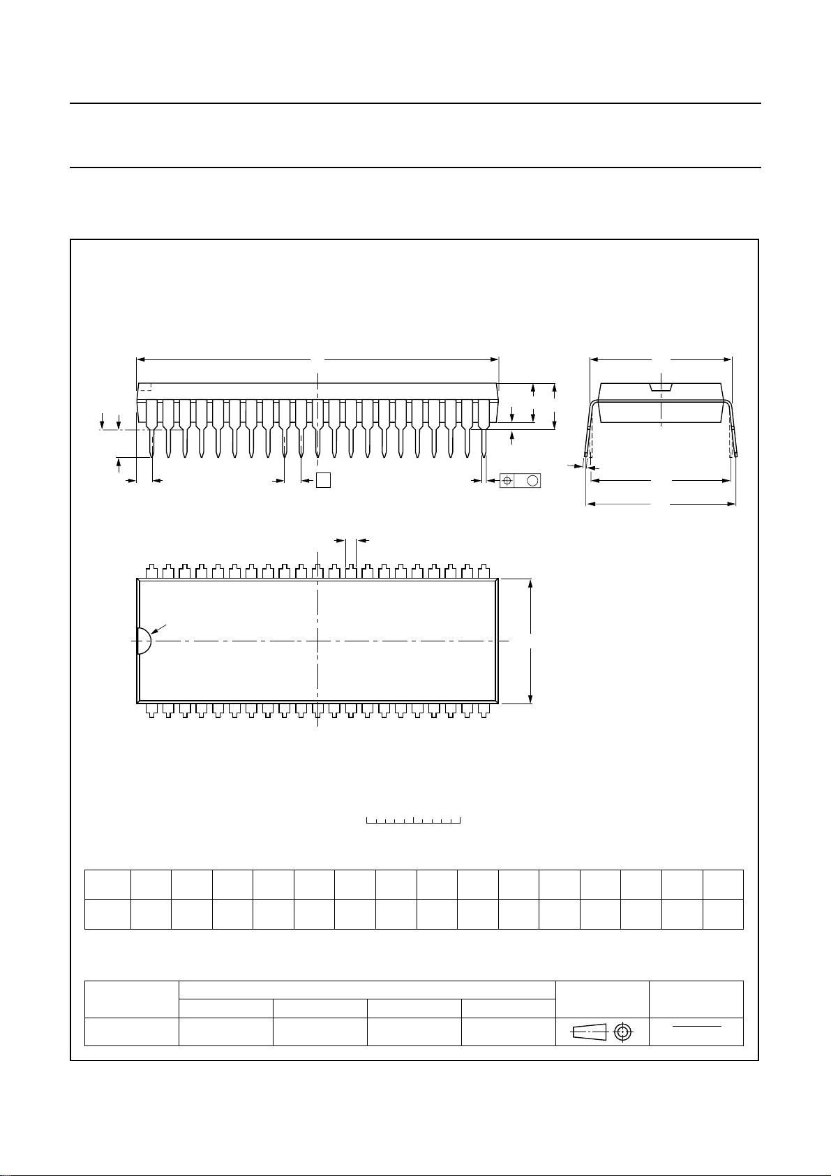
Philips Semiconductors Preliminary specification
Universal Serial Bus (USB) CODEC UDA1325
PACKAGE OUTLINES
SDIP42: plastic shrink dual in-line package; 42 leads (600 mil)
D
seating plane
L
Z
42
pin 1 index
e
b
SOT270-1
M
E
A
2
A
A
1
w M
b
1
22
E
c
(e )
M
1
H
1
0 5 10 mm
scale
DIMENSIONS (mm are the original dimensions)
A
A
A
UNIT b
Note
1. Plastic or metal protrusions of 0.25 mm maximum per side are not included.
max.
mm
5.08 0.51 4.0
OUTLINE
VERSION
SOT270-1
12
min.
max.
IEC JEDEC EIAJ
1.3
0.8
b
1
0.53
0.40
REFERENCES
0.32
0.23
cEe M
(1) (1)
D
38.9
38.4
1999 May 10 47
14.0
13.7
21
(1)
Z
1
L
M
E
3.2
15.80
2.9
15.24
EUROPEAN
PROJECTION
17.15
15.90
e
w
H
0.181.778 15.24
ISSUE DATE
90-02-13
95-02-04
max.
1.73
Page 48
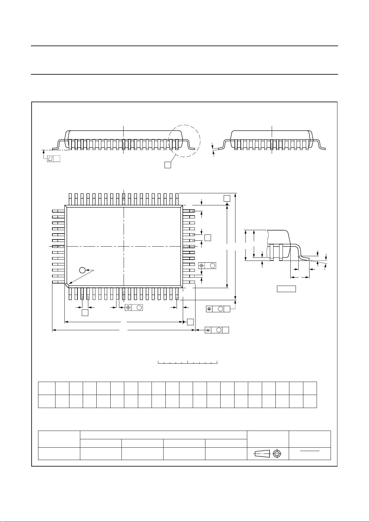
Philips Semiconductors Preliminary specification
Universal Serial Bus (USB) CODEC UDA1325
QFP64: plastic quad flat package; 64 leads (lead length 1.95 mm); body 14 x 20 x 2.8 mm
c
y
X
51 33
52
pin 1 index
64
1
32
Z
e
w M
b
p
20
19
A
E
A
H
E
2
A
E
A
1
detail X
L
p
L
SOT319-2
(A )
3
θ
w M
b
e
p
Z
D
D
H
D
0 5 10 mm
scale
DIMENSIONS (mm are the original dimensions)
mm
A
max.
3.20
0.25
0.05
2.90
2.65
0.25
0.50
0.35
0.25
0.14
UNIT A1A2A3bpcE
(1)
(1) (1)(1)
D
20.1
19.9
eH
H
14.1
13.9
24.2
1
23.6
Note
1. Plastic or metal protrusions of 0.25 mm maximum per side are not included.
OUTLINE
VERSION
IEC JEDEC EIAJ
REFERENCES
SOT319-2
1999 May 10 48
D
B
E
18.2
17.6
v M
A
v M
B
LL
p
1.0
0.6
0.2 0.10.21.95
EUROPEAN
PROJECTION
Z
D
1.2
0.8
Zywv θ
E
o
1.2
7
o
0.8
0
ISSUE DATE
95-02-04
97-08-01
Page 49

Philips Semiconductors Preliminary specification
Universal Serial Bus (USB) CODEC UDA1325
SOLDERING
Introduction
This text gives a very brief insight to a complex technology.
A more in-depth account of soldering ICs can be found in
“Data Handbook IC26; Integrated Circuit Packages”
our
(document order number 9398 652 90011).
There is no soldering method that is ideal for all IC
packages. Wave soldering is often preferred when
through-hole and surface mount components are mixed on
one printed-circuit board. However, wave soldering is not
always suitable for surface mount ICs, or for printed-circuit
boards with high population densities. In these situations
reflow soldering is often used.
Through-hole mount packages
S
OLDERING BY DIPPING OR BY SOLDER WAVE
The maximum permissible temperature of the solder is
260 °C; solder at this temperature must not be in contact
with the joints for more than 5 seconds. The total contact
time of successive solder waves must not exceed
5 seconds.
The device may be mounted up to the seating plane, but
the temperature of the plastic body must not exceed the
specified maximum storage temperature (T
stg(max)
). If the
printed-circuit board has been pre-heated, forced cooling
may be necessary immediately after soldering to keep the
temperature within the permissible limit.
M
ANUAL SOLDERING
Apply the soldering iron (24 V or less) to the lead(s) of the
package, either below the seating plane or not more than
2 mm above it. If the temperature of the soldering iron bit
is less than 300 °C it may remain in contact for up to
10 seconds. If the bit temperature is between
300 and 400 °C, contact may be up to 5 seconds.
Surface mount packages
REFLOW SOLDERING
Reflow soldering requires solder paste (a suspension of
fine solder particles, flux and binding agent) to be applied
to the printed-circuit board by screen printing, stencilling or
pressure-syringe dispensing before package placement.
Several methods exist for reflowing; for example,
infrared/convection heating in a conveyor type oven.
Throughput times (preheating, soldering and cooling) vary
between 100 and 200 seconds depending on heating
method.
Typical reflow peak temperatures range from
215 to 250 °C. The top-surface temperature of the
packages should preferable be kept below 230 °C.
W
AVE SOLDERING
Conventional single wave soldering is not recommended
for surface mount devices (SMDs) or printed-circuit boards
with a high component density, as solder bridging and
non-wetting can present major problems.
To overcome these problems the double-wave soldering
method was specifically developed.
If wave soldering is used the following conditions must be
observed for optimal results:
• Use a double-wave soldering method comprising a
turbulent wave with high upward pressure followed by a
smooth laminar wave.
• For packages with leads on two sides and a pitch (e):
– larger than or equal to 1.27 mm, the footprint
longitudinal axis is preferred to be parallel to the
transport direction of the printed-circuit board;
– smaller than 1.27 mm, the footprint longitudinal axis
must be parallel to the transport direction of the
printed-circuit board.
The footprint must incorporate solder thieves at the
downstream end.
• For packages with leads on four sides, the footprint must
be placed at a 45° angle to the transport direction of the
printed-circuit board. The footprint must incorporate
solder thieves downstream and at the side corners.
During placement and before soldering, the package must
be fixed with a droplet of adhesive. The adhesive can be
applied by screen printing, pin transfer or syringe
dispensing. The package can be soldered after the
adhesive is cured.
Typical dwell time is 4 seconds at 250 °C.
A mildly-activated flux will eliminate the need for removal
of corrosive residues in most applications.
M
ANUAL SOLDERING
Fix the component by first soldering two
diagonally-opposite end leads. Use a low voltage (24 V or
less) soldering iron applied to the flat part of the lead.
Contact time must be limited to 10 seconds at up to
300 °C.
When using a dedicated tool, all other leads can be
soldered in one operation within 2 to 5 seconds between
270 and 320 °C.
1999 May 10 49
Page 50

Philips Semiconductors Preliminary specification
Universal Serial Bus (USB) CODEC UDA1325
Suitability of IC packages for wave, reflow and dipping soldering methods
MOUNTING PACKAGE
Through-hole mount DBS, DIP, HDIP, SDIP, SIL suitable
WAVE REFLOW
(2)
− suitable
(1)
DIPPING
Surface mount BGA, SQFP not suitable suitable −
SOLDERING METHOD
HLQFP, HSQFP, HSOP, HTSSOP, SMS not suitable
(4)
PLCC
, SO, SOJ suitable suitable −
LQFP, QFP, TQFP not recommended
SSOP, TSSOP, VSO not recommended
(3)
(4)(5)
(6)
suitable −
suitable −
suitable −
Notes
1. All surface mount (SMD) packages are moisture sensitive. Depending upon the moisture content, the maximum
temperature (with respect to time) and body size of the package, there is a risk that internal or external package
cracks may occur due to vaporization of the moisture in them (the so called popcorn effect). For details, refer to the
Drypack information in the
“Data Handbook IC26; Integrated Circuit Packages; Section: Packing Methods”
.
2. For SDIP packages, the longitudinal axis must be parallel to the transport direction of the printed-circuit board.
3. These packages are not suitable for wave soldering as a solder joint between the printed-circuit board and heatsink
(at bottom version) can not be achieved, and as solder may stick to the heatsink (on top version).
4. If wave soldering is considered, then the package must be placed at a 45° angle to the solder wave direction.
The package footprint must incorporate solder thieves downstream and at the side corners.
5. Wave soldering is only suitable for LQFP, QFP and TQFP packages with a pitch (e) equal to or larger than 0.8 mm;
it is definitely not suitable for packages with a pitch (e) equal to or smaller than 0.65 mm.
6. Wave soldering is only suitable for SSOP and TSSOP packages with a pitch (e) equal to or larger than 0.65 mm; it is
definitely not suitable for packages with a pitch (e) equal to or smaller than 0.5 mm.
1999 May 10 50
Page 51

Philips Semiconductors Preliminary specification
Universal Serial Bus (USB) CODEC UDA1325
DEFINITIONS
Data sheet status
Objective specification This data sheet contains target or goal specifications for product development.
Preliminary specification This data sheet contains preliminary data; supplementary data may be published later.
Product specification This data sheet contains final product specifications.
Limiting values
Limiting values given are in accordance with the Absolute Maximum Rating System (IEC 134). Stress above one or
more of the limiting values may cause permanent damage to the device. These are stress ratings only and operation
of the device at these or at any other conditions above those given in the Characteristics sections of the specification
is not implied. Exposure to limiting values for extended periods may affect device reliability.
Application information
Where application information is given, it is advisory and does not form part of the specification.
LIFE SUPPORT APPLICATIONS
These products are not designed for use in life support appliances, devices, or systems where malfunction of these
products can reasonably be expected to result in personal injury. Philips customers using or selling these products for
use in such applications do so at their own risk and agree to fully indemnify Philips for any damages resulting from such
improper use or sale.
2
PURCHASE OF PHILIPS I
C COMPONENTS
2
Purchase of Philips I
components in the I2C system provided the system conforms to the I2C specification defined by
Philips. This specification can be ordered using the code 9398 393 40011.
C components conveys a license under the Philips’ I2C patent to use the
1999 May 10 51
Page 52

Philips Semiconductors – a worldwide company
Argentina: see South America
Australia: 34 Waterloo Road, NORTH RYDE, NSW 2113,
Tel. +61 2 9805 4455, Fax. +61 2 9805 4466
Austria: Computerstr. 6, A-1101 WIEN, P.O. Box 213,
Tel. +43 1 60 101 1248, Fax. +43 1 60 101 1210
Belarus: Hotel Minsk Business Center, Bld. 3, r. 1211, Volodarski Str. 6,
220050 MINSK, Tel. +375 172 20 0733, Fax. +375 172 20 0773
Belgium: see The Netherlands
Brazil: see South America
Bulgaria: Philips Bulgaria Ltd., Energoproject, 15th floor,
51 James Bourchier Blvd., 1407 SOFIA,
Tel. +359 2 68 9211, Fax. +359 2 68 9102
Canada: PHILIPS SEMICONDUCTORS/COMPONENTS,
Tel. +1 800 234 7381, Fax. +1 800 943 0087
China/Hong Kong: 501 Hong Kong Industrial Technology Centre,
72 Tat Chee Avenue, Kowloon Tong, HONG KONG,
Tel. +852 2319 7888, Fax. +852 2319 7700
Colombia: see South America
Czech Republic: see Austria
Denmark: Sydhavnsgade 23, 1780 COPENHAGEN V,
Tel. +45 33 29 3333, Fax. +45 33 29 3905
Finland: Sinikalliontie 3, FIN-02630 ESPOO,
Tel. +358 9 615 800, Fax. +358 9 6158 0920
France: 51 Rue Carnot, BP317, 92156 SURESNES Cedex,
Tel. +33 1 4099 6161, Fax. +33 1 4099 6427
Germany: Hammerbrookstraße 69, D-20097 HAMBURG,
Tel. +49 40 2353 60, Fax. +49 40 2353 6300
Hungary: see Austria
India: Philips INDIA Ltd, Band Box Building, 2nd floor,
254-D, Dr. Annie Besant Road, Worli, MUMBAI 400 025,
Tel. +91 22 493 8541, Fax. +91 22 493 0966
Indonesia: PT Philips Development Corporation, Semiconductors Division,
Gedung Philips, Jl. Buncit Raya Kav.99-100, JAKARTA 12510,
Tel. +62 21 794 0040 ext. 2501, Fax. +62 21 794 0080
Ireland: Newstead, Clonskeagh, DUBLIN 14,
Tel. +353 1 7640 000, Fax. +353 1 7640 200
Israel: RAPAC Electronics, 7 Kehilat Saloniki St, PO Box 18053,
TEL AVIV 61180, Tel. +972 3 645 0444, Fax. +972 3 649 1007
Italy: PHILIPS SEMICONDUCTORS, Piazza IV Novembre 3,
20124 MILANO, Tel. +39 02 67 52 2531, Fax. +39 02 67 52 2557
Japan: Philips Bldg 13-37, Kohnan 2-chome, Minato-ku,
TOKYO 108-8507, Tel. +81 3 3740 5130, Fax. +81 3 3740 5077
Korea: Philips House, 260-199 Itaewon-dong, Yongsan-ku, SEOUL,
Tel. +82 2 709 1412, Fax. +82 2 709 1415
Malaysia: No. 76 Jalan Universiti, 46200 PETALING JAYA, SELANGOR,
Tel. +60 3 750 5214, Fax. +60 3 757 4880
Mexico: 5900 Gateway East, Suite 200, EL PASO, TEXAS 79905,
Tel. +9-5 800 234 7381, Fax +9-5 800 943 0087
Middle East: see Italy
Netherlands: Postbus 90050, 5600PB EINDHOVEN, Bldg. VB,
Tel. +31 40 27 82785, Fax. +31 40 27 88399
New Zealand: 2 Wagener Place, C.P.O. Box 1041, AUCKLAND,
Tel. +64 9 849 4160, Fax. +64 9 849 7811
Norway: Box 1, Manglerud 0612, OSLO,
Tel. +47 22 74 8000, Fax. +47 22 74 8341
Pakistan: see Singapore
Philippines: Philips Semiconductors Philippines Inc.,
106 Valero St. Salcedo Village, P.O. Box 2108 MCC, MAKATI,
Metro MANILA, Tel. +63 2 816 6380, Fax. +63 2 817 3474
Poland: Ul. Lukiska 10, PL 04-123 WARSZAWA,
Tel. +48 22 612 2831, Fax. +48 22 612 2327
Portugal: see Spain
Romania: see Italy
Russia: Philips Russia, Ul. Usatcheva 35A, 119048 MOSCOW,
Tel. +7 095 755 6918, Fax. +7 095 755 6919
Singapore: Lorong 1, Toa Payoh, SINGAPORE 319762,
Tel. +65 350 2538, Fax. +65 251 6500
Slovakia: see Austria
Slovenia: see Italy
South Africa: S.A. PHILIPS Pty Ltd., 195-215 Main Road Martindale,
2092 JOHANNESBURG, P.O. Box 58088 Newville 2114,
Tel. +27 11 471 5401, Fax. +27 11 471 5398
South America: Al. Vicente Pinzon, 173, 6th floor,
04547-130 SÃO PAULO, SP, Brazil,
Tel. +55 11 821 2333, Fax. +55 11 821 2382
Spain: Balmes 22, 08007 BARCELONA,
Tel. +34 93 301 6312, Fax. +34 93 301 4107
Sweden: Kottbygatan 7, Akalla, S-16485 STOCKHOLM,
Tel. +46 8 5985 2000, Fax. +46 8 5985 2745
Switzerland: Allmendstrasse 140, CH-8027 ZÜRICH,
Tel. +41 1 488 2741 Fax. +41 1 488 3263
Taiwan: Philips Semiconductors, 6F, No. 96, Chien Kuo N. Rd., Sec. 1,
TAIPEI, Taiwan Tel. +886 2 2134 2886, Fax. +886 2 2134 2874
Thailand: PHILIPS ELECTRONICS (THAILAND) Ltd.,
209/2 Sanpavuth-Bangna Road Prakanong, BANGKOK 10260,
Tel. +66 2 745 4090, Fax. +66 2 398 0793
Turkey: Yukari Dudullu, Org. San. Blg., 2.Cad. Nr. 28 81260 Umraniye,
ISTANBUL, Tel. +90 216 522 1500, Fax. +90 216 522 1813
Ukraine: PHILIPS UKRAINE, 4 Patrice Lumumba str., Building B, Floor 7,
252042 KIEV, Tel. +380 44 264 2776, Fax. +380 44 268 0461
United Kingdom: Philips Semiconductors Ltd., 276 Bath Road, Hayes,
MIDDLESEX UB3 5BX, Tel. +44 181 730 5000, Fax. +44 181 754 8421
United States: 811 East Arques Avenue, SUNNYVALE, CA 94088-3409,
Tel. +1 800 234 7381, Fax. +1 800 943 0087
Uruguay: see South America
Vietnam: see Singapore
Yugoslavia: PHILIPS, Trg N. Pasica 5/v, 11000 BEOGRAD,
Tel. +381 11 62 5344, Fax.+381 11 63 5777
For all other countries apply to: Philips Semiconductors,
International Marketing & Sales Communications, Building BE-p, P.O. Box 218,
5600 MD EINDHOVEN, The Netherlands, Fax. +31 40 27 24825
© Philips Electronics N.V. SCA
All rights are reserved. Reproduction in whole or in part is prohibited without the prior written consent of the copyright owner.
The information presented in this document does not form part of any quotation or contract, is believed to be accurate and reliable and may be changed
without notice. No liability will be accepted by the publisher for any consequence of its use. Publication thereof does not convey nor imply any license
under patent- or other industrial or intellectual property rights.
1999 64
Internet: http://www.semiconductors.philips.com
Printed in The Netherlands 545002/750/01/pp52 Date of release: 1999 May 10 Document order number: 9397 750 02805
 Loading...