

Page 1

查询UAA3580供应商
INTEGRATED CIRCUITS
DATA SH EET
UAA3580
Wideband code division multiple
access frequency division duplex
zero IF receiver
Objective specification
Supersedes data of 2002 Oct 16
2002 Oct 30
Page 2

Philips Semiconductors Objective specification
Wideband code division multiple access
frequency division duplex zero IF receiver
CONTENTS
1 FEATURES
2 APPLICATIONS
3 GENERAL DESCRIPTION
4 QUICK REFERENCE DATA
5 ORDERING INFORMATION
6 BLOCK DIAGRAM
7 PINNING INFORMATION
7.1 Pinning
7.2 Pin description
8 FUNCTIONAL DESCRIPTION
8.1 RF receiver front-end and RF VCO
8.2 Channel filter and AGC
8.3 RF VCO
8.4 RF LO section
8.5 RF fractional-N synthesizer PLL
8.6 Clock PLL
8.7 Control
9 OPERATING MODES
9.1 Basic operating mode
9.2 AGC gain look-up table
9.3 RF PLL synthesizer
9.4 Clock PLL synthesizer
10 PROGRAMMING
10.1 Serial programming bus
10.2 Data format
10.3 Register contents
11 LIMITING VALUES
12 THERMAL CHARACTERISTICS
13 DC CHARACTERISTICS
14 AC CHARACTERISTICS
15 SERIAL BUS TIMING CHARACTERISTICS
16 APPLICATION INFORMATION
17 PACKAGE OUTLINE
18 SOLDERING
18.1 Introduction to soldering surface mount
18.2 Reflow soldering
18.3 Wave soldering
18.4 Manual soldering
18.5 Suitability of surface mount IC packages for
19 DATA SHEET STATUS
20 DEFINITIONS
21 DISCLAIMERS
UAA3580
packages
wave and reflow soldering methods
2002 Oct 30 2
Page 3
Philips Semiconductors Objective specification
Wideband code division multiple access
frequency division duplex zero IF receiver
1 FEATURES
• Low noise wide dynamic range for zero IF receivers
• 79 dB gain control range; in steps of 1 dB
• Channel filters
• 96 dB voltage gain
• Fully integrated fractional-N synthesizer with AFC
control capability
• Fully integrated RF VCO withintegrated supply voltage
regulator
• Fully differential design to minimize crosstalk
• Supply voltage from 2.4 to 3.3 V
• 3-wire serial interface bus
• HVQFN24 package.
2 APPLICATIONS
• WCDM-FDDreceiver for GSM hand-portable equipment
• Dual mode GSM/GPRS/EDGE/UMTS handset.
UAA3580
3 GENERAL DESCRIPTION
The UAA3580 is a BiCMOS integrated circuit receiver
intended for the Third Generation Partnership Project
(3GPP) specification for the Universal Mobile
Telecommunication System (UMTS).
ThecircuitisspeciallydesignedfortheFrequencyDivision
Duplex (FDD) mode of the Wide Code Division Multiple
Access (WCDMA) that operates in the 2110 to 2170 MHz
band.
The UAA3580 contains the whole analog receive chain
from Radio Frequency (RF) Low Noise Amplifier (LNA) to
baseband IQ outputs including a channel filter, a complete
RF Phase-Locked Loop (PLL) with a fully integrated
Voltage Controlled Oscillator (VCO), and a clock PLL that
generates a programmable UMTS system clock from an
external 26 MHz reference signal.
4 QUICK REFERENCE DATA
SYMBOL PARAMETER MIN. TYP. MAX. UNIT
V
CCA
V
DDD
T
amb
5 ORDERING INFORMATION
TYPE
NUMBER
UAA3580HN HVQFN24 plastic, heatsink very thin quad flat package; no leads
analog supply voltage 2.6 − 3.3 V
digital supply voltage 1.6 − 2.8 V
ambient temperature −30 − +70 °C
PACKAGE
VERSION
NAME DESCRIPTION
SOT616-1
24 terminals; body 4 × 4 × 0.90 mm
2002 Oct 30 3
Page 4
Philips Semiconductors Objective specification
Wideband code division multiple access
frequency division duplex zero IF receiver
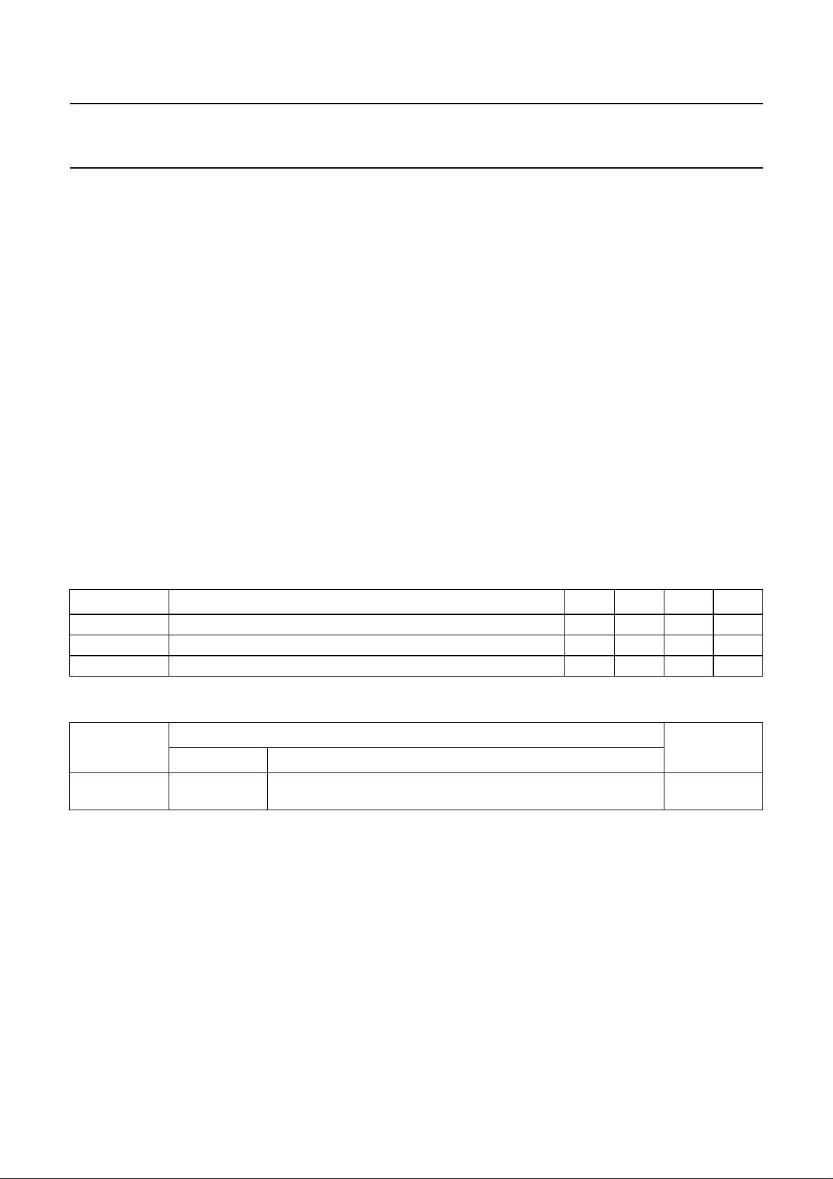
6 BLOCK DIAGRAM
handbook, full pagewidth
REFIN
V
CCA(SYN)
CPCLKO
V
CCA(CP)
RFCPO
CAPVCOREG
VCOGND
V
CCA(RF)
RFGND
RFIP
RFIN
IFGND
RXCEN
V
CCA(IF)
19
20
21
22
23
24
1
2
3
4
5
6
7
8
SIGMA DELTA
FRACTIONAL-N
RF VCO
VCO
REGULATOR
LNA
RF
DIVIDE-BY-2
MIXER
MIXER
RF
SIGMA DELTA
FRACTIONAL-N
UAA3580HN
DIVIDE-BY-2
VCO
SERIAL INTERFACE
18
17
16
15
14
13
12
11
10
9
REXT
UMTSCLKO
V
DDD
EN
CLK
DATA
QN
QP
IN
IP
FCA236
UAA3580
Fig.1 Block diagram.
2002 Oct 30 4
Page 5
Philips Semiconductors Objective specification
Wideband code division multiple access
frequency division duplex zero IF receiver
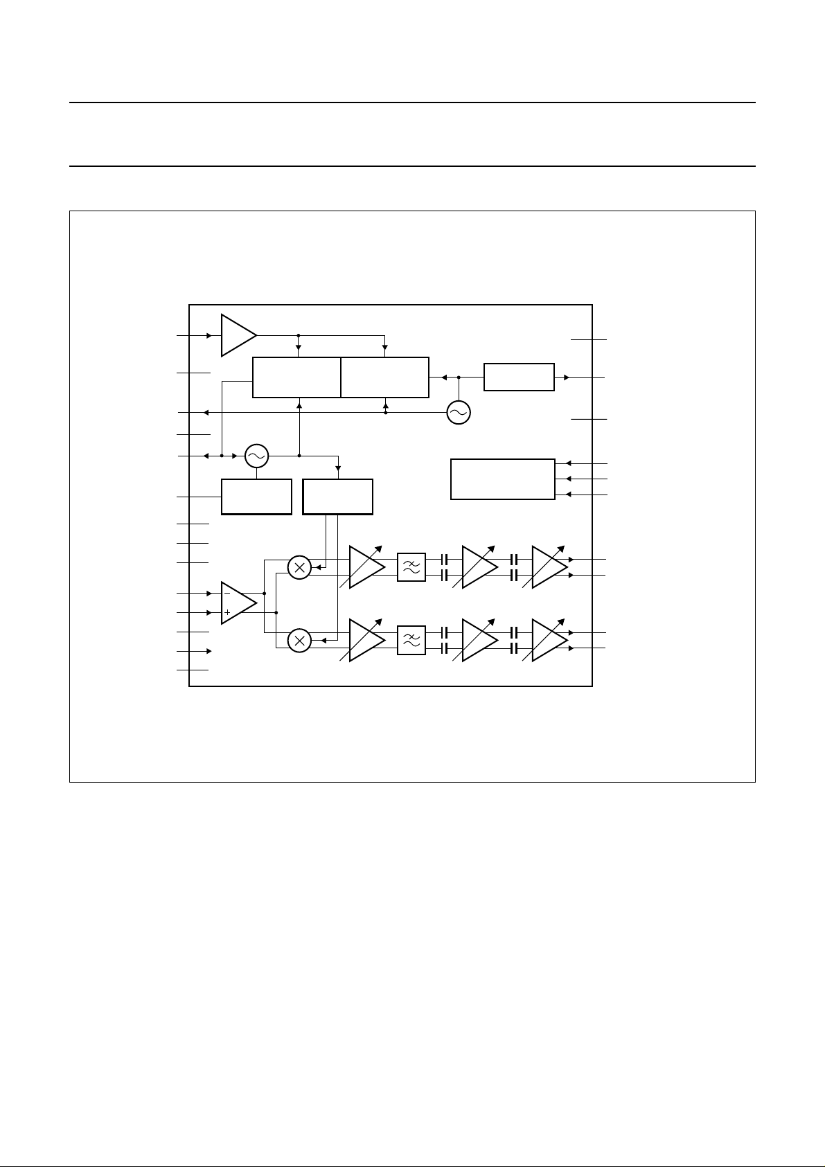
7 PINNING INFORMATION
7.1 Pinning
handbook, full pagewidth
IFGND
RFIN
RFIP
RFGND
V
CCA(RF)
VCOGND
6
5
4
3
2
1
CCA(IF)
V
RXCEN
8
7
UAA3580HN
UAA3580
IP
IN
9
10
QP
11
QN
12
13
DATA
14
CLK
15
EN
V
16
UMTSCLKO
17
REXT
18
DDD
22
23
24
RFCPO
CCA(CP)
V
CAPVCOREG
20
21
CPCLKO
CCA(SYN)
V
Fig.2 Pin configuration.
19
FCA237
REFIN
2002 Oct 30 5
Page 6

Philips Semiconductors Objective specification
Wideband code division multiple access
frequency division duplex zero IF receiver
7.2 Pin description
Table 1 HVQFN24 package
SYMBOL PIN DESCRIPTION
VCOGND 1 RF VCO ground
V
CCA(RF)
RFGND 3 RF receiver ground
RFIP 4 RF positive input
RFIN 5 RF negative input
IFGND 6 IF section ground
RXCEN 7 receiver chip enable input
V
CCA(IF)
IP 9 differential receive baseband positive in-phase output
IN 10 differential receive baseband negative in-phase output
QP 11 differential receive baseband positive in-quadrature output
QN 12 differential receive baseband negative in-quadrature output
DATA 13 serial bus data input
CLK 14 serial bus clock input
EN 15 serial bus enable input
V
DDD
UMTSCLKO 17 UMTS system clock output
REXT 18 external charge pump biasing resistor connection
REFIN 19 reference clock input
V
CCA(SYN)
CPCLKO 21 charge pump clock output
V
CCA(CP)
RFCPO 23 RF charge pump output
CAPVCOREG 24 decoupling capacitor for the VCO regulator
2 analog supply voltage for the RF receiver
8 analog supply voltage for the IF section
16 digital supply voltage
20 analog supply voltage for the synthesizer
22 analog supply voltage for the charge pump section
die pad ground
UAA3580
2002 Oct 30 6
Page 7

Philips Semiconductors Objective specification
Wideband code division multiple access
frequency division duplex zero IF receiver
8 FUNCTIONAL DESCRIPTION
The receiver consists of an RF receiver front-end, an
RF VCO, a channel filter, Automatic Gain Control (AGC),
a RF fractional-N synthesizer PLL, a clock PLL, a
Power-up reset circuit and a 3-wire serial programming
bus.
8.1 RF receiver front-end and RF VCO
The front-end receiver converts the aerial RF signal from
WCMDA (2.11 to 2.17 GHz) band down to a Zero
Intermediate Frequency (ZIF). The first stage is a
differential low noise amplifier matched to 50 Ω using an
external balun. The LNA is followed by an IQ down-mixer
which consists of two mixers in parallel but driven by
quadrature out-of-phase LO signals. The In phase (I) and
Quadrature phase (Q) ZIF signals are then low-pass
filtered, to provide protection from high frequency offset
interference, and fed into the channel filter.
8.2 Channel filter and AGC
The front-end zero IF I and Q outputs are applied to the
integrated low-pass channel filter with a provision for
4 × 8 dB gain steps in front of the filter. The filter is a
self-calibrated fifth-order low-pass filter with a cut-off
frequency around 2.4 MHz. Once filtered the zero IF
I and Q outputs are further amplified with provision for
47 × 1 dB steps and DC offset compensation. The zero IF
output buffer provides close rail-to-rail output signal.
8.3 RF VCO
The RF VCO is fully integrated and self-calibrated on
manufacturing tolerances. It consists of 16 different
frequency ranges that are selected internally, depending
on the frequency programmation. It covers the necessary
bandwidth of 4.22 to 4.34 GHz and is tuned via the RF
charge pump and external loop filter. An internal supply
voltage regulator using the pin CAPVCOREG as external
decoupling capacitor supplies the RF VCO and minimizes
parasitic coupling and pushing. The regulator and the RF
VCO are turned on by the RXCEN signal.
8.4 RF LO section
The RF LO section covering the 4.22 to 4.34 GHz band is
driven by the internal RF VCO module. It includes the LO
buffering for the RF PLL and a divide-by-two circuit to
generate the quadrature LO signals to drive the RX IQ
down-mixer.
UAA3580
8.5 RF fractional-N synthesizer PLL
A high performance RF fractional-N synthesizer PLL is
included on-chip which enables the frequency of the RF
VCOtobesynthesized.Thefrequencyissetviathe3-wire
serial programming bus.
The PLL is based on Sigma-Delta (Σ∆) fractional-N
synthesis that enables the required channel frequency,
including Automatic Frequency Control (AFC) from a free
running external 26 MHz GSM reference frequency, to be
obtained. Very low close in-phase noise is achieved which
allows a wider PLL loop bandwidth and a shorter settling
time. The programmable main dividers are controlled by a
second-order (Σ∆) modulus controller. They divide the RF
VCO signals down to frequencies of 26 MHz (in
programmable 12 Hz steps). Their phase is then
compared in a digital Phase/Frequency Detector (PFD) to
the 26 MHz reference clock signal. The phase error
informationis fed back to the RF VCO viathecharge pump
circuit that ‘sources’ into or ‘sinks’ current from the loop
filter capacitor, thus changing the VCO frequency so that
the loop is finally brought into phase-lock.
The RF synthesizer division range enables an external
reference frequency of 13 to 26 MHz to be used.
8.6 Clock PLL
The clock PLL is based on SD fractional-N synthesis that
allows the UMTS system clock, including AFC from a
non-correctedexternal 26 MHz GSM reference frequency,
to be obtained. The PLL comprises a fully integrated RC
VCO.The PLL output is a low harmonic content waveform,
the frequency of which can be programmed to
15.36, 30.72 or 61.44 MHz. The default value is
30.72 MHz.
8.7 Control
Thecontrolof the chip is done via the 3-wire serial bus and
pin RXCEN. At power-up the clock PLL section is
automatically enabled, the other sections are enabled
when the RXCEN signal is set HIGH (also via the 3-wire
bus). The power-up signal is detected on pin V
the voltage rises. The V
maintained, enables the programming parameters to be
retained in memory.
pin, if the supply voltage is
DDD
DDD
when
2002 Oct 30 7
Page 8
Philips Semiconductors Objective specification
Wideband code division multiple access
UAA3580
frequency division duplex zero IF receiver
9 OPERATING MODES
9.1 Basic operating modes
The circuit can be powered up into different operating
modes, depending on the control bits RXON and SYNON,
via the 3-wire bus. This defines three main modes called
IDLE, SYN and RX mode.
The voltage level applied to pin RXCEN must be set HIGH
to enable the device. The VCO and the PLL sections are
enabled in SYN mode. In the RX mode every section is
enabled (receive part, VCO and PLL sections).
Table 3 AGC gain look-up table
AGC8 AGC7 AGC6 AGC5 AGC4 AGC3 AGC2 AGC1 AGC0
111111111 0
111111110 1
111111101 2
111111100 3
111111011 4
111111010 5
111111001 6
111111000 7
111110111 8
111110110 9
111110101 10
111110100 11
101111011 12
101111010 13
101111001 14
101111000 15
101110111 16
101110110 17
101110101 18
101110100 19
011111011 20
011111010 21
011111001 22
011111000 23
011110111 24
011110110 25
011110101 26
011110100 27
001111011 28
001111010 29
Table 2 Selection of operating mode
MODE SYNON RXON
IDLE 0 0
SYN 1 0
RX 1 1
9.2 AGC gain look-up table
The AGC gain is set via the AGC[8:0] bits; see Table 3.
ATTENUATION FROM
MAXIMUM GAIN (dB)
2002 Oct 30 8
Page 9

Philips Semiconductors Objective specification
Wideband code division multiple access
UAA3580
frequency division duplex zero IF receiver
AGC8 AGC7 AGC6 AGC5 AGC4 AGC3 AGC2 AGC1 AGC0
001111001 30
001111000 31
001110111 32
001110110 33
001110101 34
001110100 35
000111011 36
000111010 37
000111001 38
000111000 39
000110111 40
000110110 41
000110101 42
000110100 43
001101011 44
001101010 45
001101001 46
001101000 47
001100111 48
001100110 49
001100101 50
001100100 51
000101011 52
000101010 53
000101001 54
000101000 55
000100111 56
000100110 57
000100101 58
000100100 59
001001011 60
001001010 61
001001001 62
001001000 63
001000111 64
001000110 65
001000101 66
001000100 67
000001011 68
000001010 69
000001001 70
ATTENUATION FROM
MAXIMUM GAIN (dB)
2002 Oct 30 9
Page 10

Philips Semiconductors Objective specification
Wideband code division multiple access
UAA3580
frequency division duplex zero IF receiver
AGC8 AGC7 AGC6 AGC5 AGC4 AGC3 AGC2 AGC1 AGC0
000001000 71
000000111 72
000000110 73
000000101 74
000000100 75
000000011 76
000000010 77
000000001 78
000000000 79
The AGC[8:0] code required to program the AGC attenuation (AGC
AGC[8:0] = (511 − AGC
AGC[8:0] = (391 − AGC
AGC[8:0] = (271 − AGC
AGC[8:0] = (151 − AGC
AGC[8:0] = (95 − AGC
AGC[8:0] = (151 − AGC
AGC[8:0] = (95 − AGC
AGC[8:0] = (135 − AGC
AGC[8:0] = (79 − AGC
if 0 < AGC
att)B
if 12 < AGC
att)B
if 20 < AGC
att)B
if 28 < AGC
att)B
if 36 < AGC
att)B
if 44 < AGC
att)B
if 52 < AGC
att)B
if 60 < AGC
att)B
if 68 < AGC
att)B
att
att
att
att
<11
att
att
att
<43
att
<59
att
<79
<19
<27
<35
<51
<67
) can be calculated from the following formulas:
att
Where (X)B is the binary code of the integer X.
ATTENUATION FROM
MAXIMUM GAIN (dB)
2002 Oct 30 10
Page 11

Philips Semiconductors Objective specification
Wideband code division multiple access
frequency division duplex zero IF receiver
9.3 RF PLL synthesizer
The RF fractional-N synthesizer is set via the 3-wire bus
with the FRAC and CH chains. CH sets the integer divider
ratio and FRAC the fractional divider ratio. They both
provide the LO frequency in accordance with the following
equation:
N
RX
f
RFLOfref
Where
K
Where KRX is the integer value of FRAC[21:0], NRX is the
integer value of CH[8:0] and f
reference applied to pin REFIN.
Example: to obtain a f
error less than ∆f
to 1290555 if the reference frequency is 26 MHz. It should
be noted that some particular frequencies can be obtained
in two ways; NRX= x and K
same frequency as NRX=x−1 and K
+
---------- 2
1
-------2
PLL NRX
K
frac(RX)
×=
22
RFLO
1
+
K
-- -
RX
2
is the external frequency
ref
frequency of 2.14 GHz with an
must be set to 164 and K
frac(RX)
×=
frac(RX)
frac(RX)
= 0.25 provides the
= 0.75
frac(RX)
UAA3580
Table 4 Clock mode
RXCEN CLKon CLKoff DESCRIPTION
1 1 0 CLKPLL synthesizer
enabled (default)
0 1 0 CLKPLL synthesizer
disabled; note 1
1 0 0 CLKPLL synthesizer
disabled; note 2
(4)
X
Notes
1. Hard power-down of the clock PLL done with RXCEN.
2. Power-down achieved via the 3-wire bus, reset by
RXCEN.
3. Power-down achieved via the 3-wire bus, no effect by
RXCEN in this mode. This mode will be reset if V
is not maintained.
4. X = don’t care.
(4)
X
1 CLKPLL synthesizer
disabled; note 3
DDD
9.4 Clock PLL synthesizer
9.4.1 AFC MODE
The clock PLL is based on the SD fractional-N synthesizer
thatallows to derivetheUMTS system clockincludingAFC
from a non-corrected external 26 MHz only GMS
reference. The clock PLL frequency with the AFC
correction word is given by the following equation:
9K
+
AFC
f
CLKPLLfref
Where
K
AFC
AFC represents the integer value of AFC[11:0] and f
×=
-----------------------
2
231
AFC
+=
------------
--------- 512
21
2
ref
is
the external reference frequency applied to pin REFIN.
9.4.2 CLOCK PLL MODES
The clock PLL synthesizer is controlled by bits CLKon and
CLKoff. At power-up the clock PLL synthesizer is
automatically on when pin RXCEN is set HIGH. The
control, done with CLKon, will be reset at the rising edge
of RXCEN. For application which do not require the UMTS
clock system, the clock PLL can be powered-down with bit
CLKoff set to logic 1.
9.4.3 CLOCK PLL OUTPUT DIVIDER
TheclockPLLoutputdividerratioissetinaccordancewith
Table 5.
Table 5 Clock mode; note 1
CLKoff CLK1 CLK0 DESCRIPTION
1 X X UMTSCLKO output
disabled
0 0 0 clock divider ratio set to
default
0 0 1 clock divider ratio set to 2
0 1 0 clock divider ratio set to 4
0 1 1 clock divider ratio set to 8
Note
1. X = don’t care.
2002 Oct 30 11
Page 12

Philips Semiconductors Objective specification
Wideband code division multiple access
frequency division duplex zero IF receiver
10 PROGRAMMING
10.1 Serial programming bus
Asimple 3-wire unidirectionalserialbus is usedtoprogram
the circuit. The 3 lines are DATA, CLK and EN.
The data sent to the device is loaded in bursts framed
by EN. Programming clock edges are ignored until EN
goes active LOW. The programmed information is loaded
into the addressed latch when EN goes HIGH (inactive).
This is allowed when CLK is in either state without causing
any consequences to the data register. Only the last
21 bits serially clocked into the device are retained within
the programming register. Additional leading bits are
ignored, and no check is made on the number of clock
pulses.
The fully static CMOS design uses virtually no current
when the bus is inactive. It can always capture new
programming data even during Power-down of the
synthesizer.
UAA3580
10.2 Data format
Data is entered with the most significant bit first. The
leading bits make up the data field, while the trailing four
bits are an address field. The address bits are decoded on
therising edge of EN. This produces an internal load pulse
to store the data in the address latch.
To ensure that data is correctly loaded on first power-up,
EN should be held LOW and only taken HIGH after having
programmed an appropriate register. To avoid erroneous
divider ratios, the pulse is inhibited during the period when
data is read by the frequency dividers. This condition is
guaranteed by respecting a minimum EN pulse width after
data transfer.
10.3 Register contents
Table 6 Register bit allocation
CONTROL BITS ADDRESS
20 19 18 17 16 15 14 13 12 11 10 9 8 7 6 5 4 3 2 1 0
for test purposes only; all bits must be set to zero for normal operation; this is a forbidden address 0 0 0 0
for test purposes only; all bits must be set to zero for normal operation; this is a forbidden address 0 0 0 1
FRAC[15:0] SYNON 0 1 0 0
CH[8:0] FR[21:16] 1 SYNON 0 1 0 1
00000 AGC[8:0] 1 1 RXON 0 1 1 0
0 AFC[11:0] CKO[1:0] CLKoff CLKon 0 1 1 1
Table 7 Description of symbols used in Table 6
SYMBOL BITS DESCRIPTION
SYNON 1 3-wire bus
RXON 1 3-wire bus
AGC 9 automatic gain control
CH 6 integer division ratio for the RF PLL
FRAC 22 fractional division ratio for the RF PLL
AFC 12 automatic frequency control for the clock PLL
CLKoff 1 clock PLL disabled
CKO 2 integer division ratio for the clock PLL
2002 Oct 30 12
Page 13

Philips Semiconductors Objective specification
Wideband code division multiple access
UAA3580
frequency division duplex zero IF receiver
Table 8 Register preset condition
CONTROL ADDRESS
20191817161514131211109876543210
000000000000000000000
000000000000000000001
000000000000000000100
000000000000000100101
000001111111111100110
010010100111000000111
11 LIMITING VALUES
In accordance with the Absolute Maximum Rating System (IEC 60134).
SYMBOL PARAMETER CONDITIONS MIN. TYP. MAX. UNIT
V
V
P
T
T
DDD
CCA
tot
amb
stg
digital supply voltage −0.3 − +2.8 V
analog supply voltage −0.3 − +3.3 V
total power dissipation −−300 mW
ambient temperature −30 − +80 °C
storage temperature −40 − +150 °C
12 THERMAL CHARACTERISTICS
SYMBOL PARAMETER CONDITIONS VALUE UNIT
R
th(j-a)
thermal resistance from
junction to ambient
in free air; on a 4 layer PCB and
with soldered exposed die pad
36 K/W
2002 Oct 30 13
Page 14

Philips Semiconductors Objective specification
Wideband code division multiple access
UAA3580
frequency division duplex zero IF receiver
13 DC CHARACTERISTICS
V
= 2.6 V; V
CCA
CCA(CP)
SYMBOL PARAMETER CONDITIONS MIN. TYP. MAX. UNIT
Supplies
V
CCA
V
DDD
I
CCA(tot)
I
CCA(RF)
I
CCA(IF)
I
CCA(SYN)
I
CCA(CP)
I
DDD
Baseband IQ section; pins IN, IP, QP and QN
V
O(IQ)(CM)
RF VCO section; pin CAPVCOREG
V
O(CAPVCOREG)
CLKPLL section; pin UMTSCLKO
V
O(UMTSCLKO)
Reference voltage; pin REXT
V
REXT
Control section; pins DATA, CLK, EN and RXON
V
IH
V
IL
= 2.6 V;T
analog supply voltage on pins V
=25°C; unless otherwise specified.
amb
V
CCA(CP)
CCA(RF)
and V
, V
CCA(IF)
CCA(SYN)
,
2.6 2.8 3.3 V
digital supply voltage 1.6 1.8 2.8 V
total analog supply current receive mode; note 1 − 52 63 mA
receive mode; note 2 − 45 54 mA
synthesizer mode; note 3 − 25 30 mA
standby mode; note 4 − 12 15 mA
sleep mode; note 5 − 10 50 µA
analog supply current for the RF
− 19 − mA
VCO section
analog supply current for the RX
− 16 − mA
section
analog supply current for the
− 15 − mA
synthesizer
analog supply current for the
− 0.9 − mA
charge pump
digital supply current − 1.1 − mA
IQ common mode output voltage 0.5(VIN+VIP) or
1.15 1.25 1.35 V
0.5(VQP+VQN); note 6
output voltage − 2 − V
output voltage − 0.8 − V
reference voltage for the charge
R
= 1.8 kΩ−360 − mV
ext
pump
HIGH-level input voltage 0.9 −−V
LOW-level input voltage −−0.3 V
Notes
1. Receive mode: All circuits are active.
2. Receive mode: All circuits are active with the clock PLL off (CLKoff = 1).
3. Synthesizer mode: RF PLL and clock PLL are active.
4. Standby mode: Clock PLL is active.
5. Sleep mode: RXCEN set LOW, DATA, CLK and EN are in high-impedance.
6. Receive mode: DC voltage supplied from the IC.
2002 Oct 30 14
Page 15

Philips Semiconductors Objective specification
Wideband code division multiple access
UAA3580
frequency division duplex zero IF receiver
14 AC CHARACTERISTICS
V
= 2.6 V; T
CCA
SYMBOL PARAMETER CONDITIONS MIN. TYP. MAX. UNIT
RF receiver inputs; pins RFIN and RFIP
f
i(RF)
R
i
C
i
s
11
F noise figure in receive mode with
CP
1
IP
3
IP
2
ϕ
n
Baseband IQ section; pins IP, IN, QP and QN
G
v(max)
G
v(min)
AGC
tot
G
step(AGC)
AGC
tot(lin)
∆G
v(IQ)
∆Φ quadrature phase error
V
o(max)
I
o(max)
V
offset(diff)
HP
−3dB
LP
−3dB
∆d
(g)
=25°C; unless otherwise specified.
amb
RF input frequency 2.11 − 2.17 GHz
input resistance − 170 −Ω
input capacitance − 1 − pF
input power matching with external balun −−10 − dB
− 3.2 4 dB
maximum gain
1 dB compression point in receive mode with
−23 −20 − dBm
maximum gain
input referred 3rd-order
intercept point
in receive mode with
maximum gain;
−18 −15 − dBm
interference 20 MHz
away from channel
bandwidth
input referred 2nd-order
intercept point
in receive mode with
maximum gain;
37 42 − dBm
interferers190 MHz away
from channel bandwidth
phase noise at 15 MHz offset −− −135 dBc/Hz
maximum voltage gain 92 96 100 dB
minimum voltage gain 12 17 22 dB
total AGC range − 79 − dB
AGC gain step − 1 − dB
total AGC linearity −0.5 − +0.5 dB
voltage gain mismatch
−− 0.5 dB
between the I and Q paths
peak error −− 5 deg
between the I and Q paths
maximum output voltage per
pin
maximum output current per
pin
differential output offset
R
=10kΩ;
L(diff)
THD < 3%
V
= 1.75 V at 1 MHz;
o(p-p)
R
=10kΩ;
L(diff)
C
=20pF
L(diff)
0.75 −− V
650 −− µA
−20 − +20 mV
voltage
−3 dB high-pass corner
frequency
−3 dB low-pass corner
frequency
2nd-order high-pass
frequency
5th-order low-pass
frequency
10 15 20 kHz
2.25 2.4 2.55 MHz
group delay variation 100 kHz < fo< 2 MHz − 260 − ns
2002 Oct 30 15
Page 16

Philips Semiconductors Objective specification
Wideband code division multiple access
UAA3580
frequency division duplex zero IF receiver
SYMBOL PARAMETER CONDITIONS MIN. TYP. MAX. UNIT
α
LPF
RF synthesizer; pin RFCPO
f
RFLO
f
comp(RF)
∆f
PLL
Φ
n
I
sink
I
source
V
o(CP)
KΦ PFD gain R
I
leak(CP)
LPF attenuation fi= 5 MHz 39 42 − dB
f
= 10 MHz 72 75 − dB
i
f
= 15 to 60 MHz 91 94 − dB
i
synthesizer frequency 2.11 − 2.17 GHz
RF comparison frequency − 26 − MHz
frequency resolution f
= 13 to 26 MHz 0.05 −− ppm
comp
=26MHz −− 6.2 Hz
f
comp
close-in-phase noise at 2 kHz offset −−85 −80 dBc/Hz
sink current R
source current R
charge pump output voltage charge pump current
= 1.8 kΩ; THD = 1% 170 200 230 µA
ext
= 1.8 kΩ; THD = 1% 170 200 230 µA
ext
0.4 − V
CCA
− 0.4 V
within specified range
= 1.8 kΩ; THD = 1% 27 32 37 µA/rad
ext
chargepump leakage current
in off state
over full charge pump
voltage range
−1 − +1 µA
N
RX
Fractional-N synthesizer; where
f
RFLOfref
×= K
---------- 2
+
K
frac(RX)
frac(RX)
1
×=
K
-------2
RX
22
1
+
-- 2
N integer divider ratio 130 − 507
K
frac
fractional divider ratio 0.25 − 0.75
Integrated RF VCO; pin RFCPO
f
RF
G
VCO
V
tune
∆f
VCC
t
cal(VCO)
RF frequency V
VCO gain V
tuning voltage 0.4 − V
pushing −− tbf MHz/V
VCO calibration time after RXON = LO ≥ HI −− 35 µs
= 0 to 3.3 V 4.22 − 4.34 GHz
RFCPO
= 1.3 V 50 70 90 MHz/V
RFCPO
CCA
CLKPLL synthesizer; pin CPCLKO
f
CLKPLL
f
comp
∆f
PLL
AFC
I
sink
I
source
V
o(CP)
cor
synthesizer frequency V
CPCLKO
= 0 to 3.3 V - 122.88 - MHz
comparison frequency − 13 − MHz
frequency resolution f
= 26 MHz 0.477 −− ppm
ref
AFC correction range −±30 − ppm
sink current R
source current R
charge pump output voltage charge pump current
= 1.8 kΩ; THD = 1% 170 200 230 µA
ext
= 1.8 kΩ; THD = 1% 170 200 230 µA
ext
0.4 − V
CCA
within specified range
KΦ PFD gain R
I
leak(CP)
chargepump leakage current
in off state
= 1.8 kΩ; THD = 1% 27 32 37 µA/rad
ext
over full charge pump
−1 − +1 µA
voltage range
− 0.4 V
− 0.4 V
2002 Oct 30 16
Page 17

Philips Semiconductors Objective specification
Wideband code division multiple access
UAA3580
frequency division duplex zero IF receiver
SYMBOL PARAMETER CONDITIONS MIN. TYP. MAX. UNIT
NK
+
AFC
Fractional-N synthesizer; where
f
CLKPLLfref
×= K
------------------------
2
AFC
N integer divider ratio − 9 −
K
AFC
fractional divider ratio 0.4512 − 0.4532
Integrated CLKPLL VCO; pin CPCLKO
f
VCO
G
V
VCO
tune
CLKPLL frequency V
VCO gain V
CPCLKO
CPCLKO
= 0 to 3.3 V 100 − 140 MHz
= 1.3 V 12 15 23 MHz/V
tuning voltage 0.4 − V
Output CLKPLL buffer; pin UMTSCLKO
f
UMTSCLKO
frequency range 15.36 30.72 61.44 MHz
N divider ratio 2 4 8
Φ
n
close-in-phase noise at 2 kHz offset for
30.72 MHz
phase noise at 3.84 MHz offset for
30.72 MHz
V
o(p-p)
output voltage (peak-to-peak
RL=10kΩ 1 −− V
value)
Low noise crystal amplifier; pin REFIN
f
REF
V
i(REF)(rms)
R
i(REF)
C
i(REF)
reference frequency 13 − 26 MHz
input voltage (RMS value) 50 − 400 mV
input resistance f
input capacitance f
= 26 MHz − tbf − kΩ
REF
= 26 MHz − tbf − pF
REF
231
AFC
+=
------------
--------- 512
21
2
− 0.4 V
CCA
−− −90 dBc/Hz
−− −110 dBc/Hz
2002 Oct 30 17
Page 18

Philips Semiconductors Objective specification
Wideband code division multiple access
UAA3580
frequency division duplex zero IF receiver
15 SERIAL BUS TIMING CHARACTERISTICS
V
= 2.6 V; V
CCA
CCA(CP)
SYMBOL PARAMETER MIN. TYP. MAX. UNIT
Serial clock; pin CLK
t
i(r)
t
i(f)
T
cyc
Enable; pin EN
t
d(START)
t
d(END)
t
W
t
su;EN
Register serial input data; pin DATA
t
su;DATA
t
h;DATA
= 2.6 V; V
DDD
= 1.6 V; T
=25°C; unless otherwise specified.
amb
input rise time −−20 ns
input fall time −−20 ns
clock period 67 −−ns
delay to rising clock edge 200 −−ns
delay from last falling clock edge 100 −−ns
minimum inactive pulse width 400 −−ns
enable set-up time to next clock 200 −−ns
input data to clock set-up time 25 −−ns
input data to clock hold time 25 −−ns
handbook, full pagewidth
CLK
DATA
EN
t
su;DAT
MSB LSB
t
d(START)
t
h;DAT
T
cyc
Fig.3 Serial bus timing diagram.
t
i(f)ti(r)
t
d(END)
ADDRESS
t
W
t
su;EN
MGU575
2002 Oct 30 18
Page 19

Philips Semiconductors Objective specification
Wideband code division multiple access
frequency division duplex zero IF receiver
16 APPLICATION INFORMATION
LC MATCH
EN
ICTL
BATTERY
antenna
or switch
3
4
5678
9
10
isolator
ceramic duplexer
1
2
UAA3592
11
12
reg
V
det
V
13 14 15 16
VCOTUNE
CCA(SYN)
V
CCA(CP)
V
CPGND
DDD
V
REFIN
CCA(SYN)
V
CPCLKO
CCA(CP)
V
RFCPO
CAPVCOREG
differential to
single-ended
SAW
CAPVCOREG
6
789101112
13
REFGND
REXT
UMTSCLKO
18
192021222324
1
VCOGND
CCA(RF)
V
RFON
5
14
V
17
2
RFGND
CCA(RF)
V
BIAS CHOKES
LC MATCH AND
RFOP
3
4
UAA3581
15
16
DDD
EN
15
16
UAA3580
3
4
RFIP
RFGND
2
17
DATA
CLK
14
5
RFIN
CCA(IF)
V
1
18
13
6
IFGND
UAA3580
FCA238
IFGND
QN
QP
IN
IP
19 20 21 22 23 24
7 8 9 10 11 12
TCEN
GSMCLKO
UMTSCLKO
REFIN
EN
CLK
DATA
QN
QP
IN
IP
CCA(IF)
V
RXCEN
handbook, full pagewidth
Fig.4 Application diagram.
This text is here in white to force landscape pages to be rotated correctly when browsing through the pdf in the Acrobat reader.This text is here in
_white to force landscape pages to be rotated correctly when browsing through the pdf in the Acrobat reader.This text is here inThis text is here in
white to force landscape pages to be rotated correctly when browsing through the pdf in the Acrobat reader. white to force landscape pages to be ...
2002 Oct 30 19
Page 20

Philips Semiconductors Objective specification
Wideband code division multiple access
frequency division duplex zero IF receiver
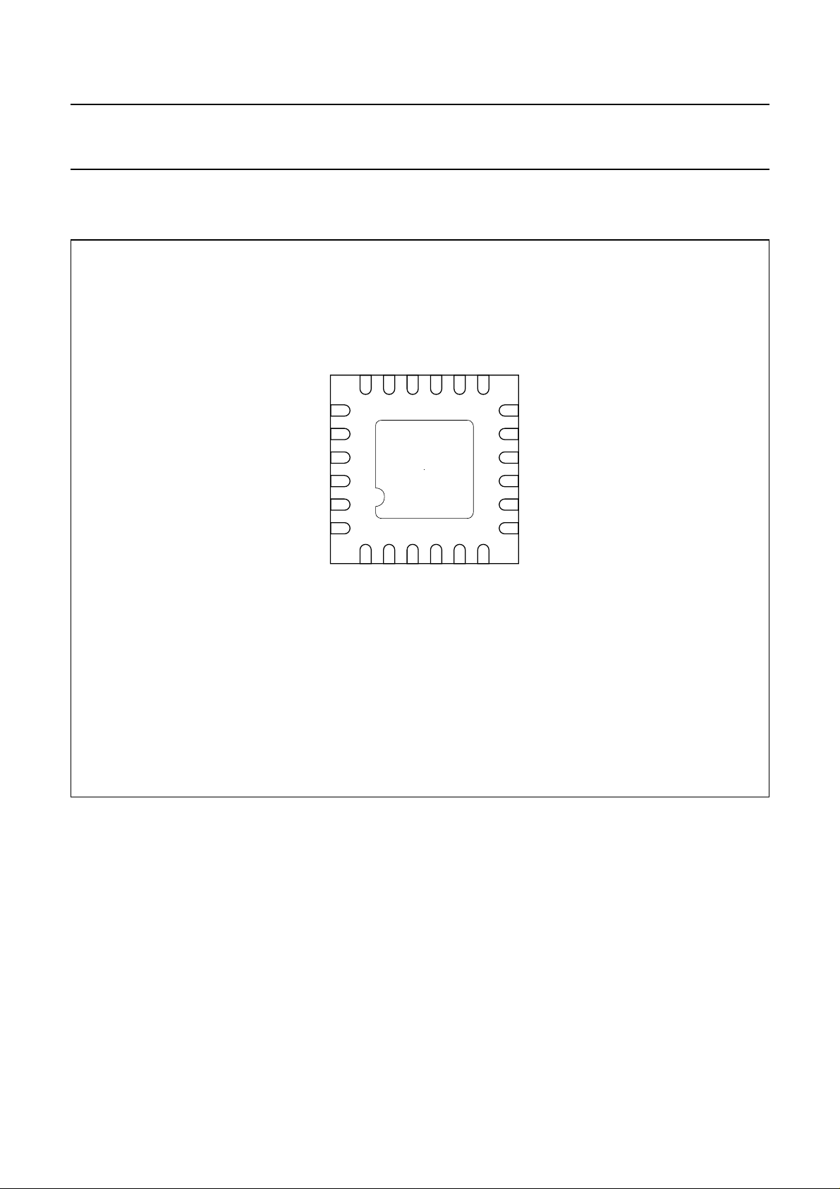
17 PACKAGE OUTLINE
HVQFN24: plastic thermal enhanced very thin quad flat package; no leads;
24 terminals; body 4 x 4 x 0.85 mm
A
D
terminal 1
index area
B
E
UAA3580
SOT616-1
A
A
1
detail X
c
e
1
1/2 e
e
712
L
6
E
h
1
terminal 1
index area
DIMENSIONS (mm are the original dimensions)
(1)
A
UNIT
mm
Note
1. Plastic or metal protrusions of 0.075 mm maximum per side are not included.
OUTLINE
VERSION
SOT616-1 MO-220 - - -- - -
max.
A
0.05
0.00
1
0.30
0.18
24
b
IEC JEDEC JEITA
(1)
c
D
4.1
2.25
3.9
1.95
b
13
e
1/2 e
18
D
h
0 2.5 5 mm
D
h
19
(1)
E
E
h
4.1
2.25
3.9
1.95
REFERENCES
scale
0.51 0.2
w
v
e
2.5
C
y
C
L
1
w
0.1v0.05
ye
0.05 0.1
EUROPEAN
PROJECTION
M
ACCB
M
e
2
e
1
2
0.5
2.5
0.3
y
X
y
1
ISSUE DATE
01-08-08
02-10-22
2002 Oct 30 20
Page 21

Philips Semiconductors Objective specification
Wideband code division multiple access
frequency division duplex zero IF receiver
18 SOLDERING
18.1 Introduction to soldering surface mount
packages
Thistext gives a very brief insighttoa complex technology.
A more in-depth account of soldering ICs can be found in
our
“Data Handbook IC26; Integrated Circuit Packages”
(document order number 9398 652 90011).
There is no soldering method that is ideal for all surface
mount IC packages. Wave soldering can still be used for
certainsurface mount ICs, but itisnot suitable for fine pitch
SMDs. In these situations reflow soldering is
recommended.
18.2 Reflow soldering
Reflow soldering requires solder paste (a suspension of
fine solder particles, flux and binding agent) to be applied
tothe printed-circuit board by screen printing, stencilling or
pressure-syringe dispensing before package placement.
Several methods exist for reflowing; for example,
convection or convection/infrared heating in a conveyor
type oven. Throughput times (preheating, soldering and
cooling) vary between 100 and 200 seconds depending
on heating method.
Typical reflow peak temperatures range from
215 to 250 °C. The top-surface temperature of the
packages should preferable be kept below 220 °C for
thick/large packages, and below 235 °C for small/thin
packages.
18.3 Wave soldering
Conventional single wave soldering is not recommended
forsurface mount devices (SMDs) orprinted-circuitboards
with a high component density, as solder bridging and
non-wetting can present major problems.
To overcome these problems the double-wave soldering
method was specifically developed.
UAA3580
If wave soldering is used the following conditions must be
observed for optimal results:
• Use a double-wave soldering method comprising a
turbulent wave with high upward pressure followed by a
smooth laminar wave.
• For packages with leads on two sides and a pitch (e):
– larger than or equal to 1.27 mm, the footprint
longitudinal axis is preferred to be parallel to the
transport direction of the printed-circuit board;
– smaller than 1.27 mm, the footprint longitudinal axis
must be parallel to the transport direction of the
printed-circuit board.
The footprint must incorporate solder thieves at the
downstream end.
• Forpackages with leads on foursides,the footprint must
be placed at a 45° angle to the transport direction of the
printed-circuit board. The footprint must incorporate
solder thieves downstream and at the side corners.
During placement and before soldering, the package must
be fixed with a droplet of adhesive. The adhesive can be
applied by screen printing, pin transfer or syringe
dispensing. The package can be soldered after the
adhesive is cured.
Typical dwell time is 4 seconds at 250 °C.
A mildly-activated flux will eliminate the need for removal
of corrosive residues in most applications.
18.4 Manual soldering
Fix the component by first soldering two
diagonally-opposite end leads. Use a low voltage (24 V or
less) soldering iron applied to the flat part of the lead.
Contact time must be limited to 10 seconds at up to
300 °C.
When using a dedicated tool, all other leads can be
soldered in one operation within 2 to 5 seconds between
270 and 320 °C.
2002 Oct 30 21
Page 22

Philips Semiconductors Objective specification
Wideband code division multiple access
UAA3580
frequency division duplex zero IF receiver
18.5 Suitability of surface mount IC packages for wave and reflow soldering methods
PACKAGE
BGA, HBGA, LFBGA, SQFP, TFBGA not suitable suitable
HBCC, HLQFP, HSQFP, HSOP, HTQFP, HTSSOP, HVQFN, SMS not suitable
(3)
PLCC
LQFP, QFP, TQFP not recommended
SSOP, TSSOP, VSO not recommended
Notes
1. All surface mount (SMD) packages are moisture sensitive. Depending upon the moisture content, the maximum
2. These packages are not suitable for wave soldering. On versions with the heatsink on the bottom side, the solder
3. If wave soldering is considered, then the package must be placed at a 45° angle to the solder wave direction.
4. Wave soldering is only suitable for LQFP, TQFP and QFP packages with a pitch (e) equal to or larger than 0.8 mm;
5. Wave soldering is only suitable for SSOP and TSSOP packages with a pitch (e) equal to or larger than 0.65 mm; it is
, SO, SOJ suitable suitable
temperature (with respect to time) and body size of the package, there is a risk that internal or external package
cracks may occur due to vaporization of the moisture in them (the so called popcorn effect). For details, refer to the
Drypack information in the
cannot penetrate between the printed-circuit board and the heatsink. On versions with the heatsink on the top side,
the solder might be deposited on the heatsink surface.
The package footprint must incorporate solder thieves downstream and at the side corners.
it is definitely not suitable for packages with a pitch (e) equal to or smaller than 0.65 mm.
definitely not suitable for packages with a pitch (e) equal to or smaller than 0.5 mm.
“Data Handbook IC26; Integrated Circuit Packages; Section: Packing Methods”
SOLDERING METHOD
WAVE REFLOW
(2)
(3)(4)
(5)
suitable
suitable
suitable
(1)
.
2002 Oct 30 22
Page 23

Philips Semiconductors Objective specification
Wideband code division multiple access
UAA3580
frequency division duplex zero IF receiver
19 DATA SHEET STATUS
LEVEL
I Objective data Development This data sheet contains data from the objective specification for product
II Preliminary data Qualification This data sheet contains data from the preliminary specification.
III Product data Production This data sheet contains data from the product specification. Philips
Notes
1. Please consult the most recently issued data sheet before initiating or completing a design.
2. The product status of the device(s) described in this data sheet may have changed since this data sheet was
3. For data sheets describing multiple type numbers, the highest-level product status determines the data sheet status.
DATA SHEET
STATUS
published. The latest information is available on the Internet at URL http://www.semiconductors.philips.com.
(1)
PRODUCT
STATUS
(2)(3)
development. Philips Semiconductors reserves the right to change the
specification in any manner without notice.
Supplementary data will be published at a later date. Philips
Semiconductors reserves the right to change the specification without
notice, in order to improve the design and supply the best possible
product.
Semiconductors reserves the right to make changes at any time in order
to improve the design, manufacturing and supply. Relevant changes will
be communicated via a Customer Product/Process Change Notification
(CPCN).
DEFINITION
20 DEFINITIONS
Short-form specification The data in a short-form
specification is extracted from a full data sheet with the
same type number and title. For detailed information see
the relevant data sheet or data handbook.
Limiting values definition Limiting values given are in
accordance with the Absolute Maximum Rating System
(IEC 60134). Stress above one or more of the limiting
values may cause permanent damage to the device.
These are stress ratings only and operation of the device
atthese or at any other conditions above thosegivenin the
Characteristics sections of the specification is not implied.
Exposure to limiting values for extended periods may
affect device reliability.
Application information Applications that are
described herein for any of these products are for
illustrative purposes only. Philips Semiconductors make
norepresentation or warranty thatsuch applications will be
suitable for the specified use without further testing or
modification.
21 DISCLAIMERS
Life support applications These products are not
designed for use in life support appliances, devices, or
systems where malfunction of these products can
reasonably be expected to result in personal injury. Philips
Semiconductorscustomers using or sellingthese products
for use in such applications do so at their own risk and
agree to fully indemnify Philips Semiconductors for any
damages resulting from such application.
Right to make changes Philips Semiconductors
reserves the right to make changes in the products including circuits, standard cells, and/or software described or contained herein in order to improve design
and/or performance. When the product is in full production
(status ‘Production’), relevant changes will be
communicated via a Customer Product/Process Change
Notification (CPCN). Philips Semiconductors assumes no
responsibility or liability for the use of any of these
products, conveys no licence or title under any patent,
copyright, or mask work right to these products, and
makes no representations or warranties that these
products are free from patent, copyright, or mask work
right infringement, unless otherwise specified.
2002 Oct 30 23
Page 24

Philips Semiconductors – a w orldwide compan y
Contact information
For additional information please visit http://www.semiconductors.philips.com. Fax: +31 40 27 24825
For sales offices addresses send e-mail to: sales.addresses@www.semiconductors.philips.com.
© Koninklijke Philips Electronics N.V. 2002
All rights are reserved. Reproduction in whole or in part is prohibited without the prior written consent of the copyright owner.
The information presented in this document does not form part of any quotation or contract, is believed to be accurate and reliable and may be changed
without notice. No liability will be accepted by the publisher for any consequence of its use. Publication thereof does not convey nor imply any license
under patent- or other industrial or intellectual property rights.
Printed in The Netherlands 403506/02/pp24 Date of release: 2002 Oct 30 Document order number: 9397 750 10632
SCA74
 Loading...