

Philips UAA2067G-C1 Datasheet

DATA SH EET
Product specification
Supersedes data of 1995 Sep 18
File under Integrated Circuits, IC17
1996 Oct 22
INTEGRATED CIRCUITS
UAA2067G
Image reject 1800 MHz transceiver
for DECT applications

1996 Oct 22 2
Philips Semiconductors Product specification
Image reject 1800 MHz transceiver
for DECT applications
UAA2067G
FEATURES
• Receiver with:
– low noise amplifier
– dual quadrature mixers for image rejection
(lower sideband)
– I and Q combining networks at a fixed IF
• Both high-frequency and low-frequency VCOs including
buffers with good isolation for low pulling
• Transmitter with:
– dual quadrature mixers for image rejection
(lower sideband)
– amplitude ramping circuit
– amplifier with high output power.
APPLICATIONS
• 1800 MHz transceiver for DECT hand-portable
equipment
• TDMA systems.
GENERAL DESCRIPTION
The UAA2067G is a low-power transceiver intended for
use in portable and base station transceivers complying
with the DECT system. The IC performs in accordance
with specifications in the −30 to +85°C temperature range.
The UAA2067G contains a front-end receiver for the
1800 to 1900 MHz frequency range, a high-frequency
VCO for the 1650 to 1850 MHz range, a low-frequency
VCO for the 100 to 140 MHz frequency range and a
transmitter with a high-output power amplifier driver stage
for the 1800 to 1900 MHz frequency range. Designed in
an advanced BiCMOS process, it combines high
performance with low-power consumption and a high
degree of integration, thus reducing external component
costs and total radio size.
Its first advantage is to provide typically 34 dB of image
rejection in the receiver path. Thus, the image filter
between the LNA and the mixer is redundant and
consequently can be removed. The receive section
consists of a low-noise amplifier that drives a quadrature
mixer pair. Image rejection is achieved by this RF mixer
pair and the two phase shifters in the I and Q channels that
phase shift the IF by 45° and 135° respectively. The two
phase shifted IFs are recombined and buffered to furnish
the IF output signal.
Signals presented at the RF input at LO − IF frequency are
rejected through this signal processing while signals at
LO + IF frequency can form the IF signal.
Its second advantage is to provide a good buffered
high-frequency VCO signal to the RX and TX mixers and
to the synthesizer-prescaler. Switching the receive or
transmit section on gives a very small change in VCO
frequency.
Its third advantage is to provide a good buffered
low-frequency VCO signal to the TX mixers, to the
synthesizer-prescaler and the second down conversion
mixer in a double conversion receiver. Switching the
transmit section on gives a very small change in
VCO frequency.
The frequency of each VCO is determined by a resonator
network that is external to the IC. Each VCO has a
regulated power supply voltage that has been designed
specifically for minimizing a change in frequency due to
changes in the power supply voltage, which may be
caused for instance by switching on the power amplifier.
Its fourth advantage is to provide typically 33 dBc of image
rejection in the single-sideband up-conversion mixer. Thus
the image filter between the power amplifier and the
antenna is redundant and may consequently be removed.
Image rejection is achieved in the internal architecture by
two RF mixers in quadrature and two phase shifters in the
low-frequency VCO signal that shifts the phase to
0° and 90°. The output signals of the mixers are summed
to form the single-upper-sideband output signal.
The output stage is a high-level output buffer with an
output power of approximately 4 dBm. The output level is
sufficient to drive a three-stage bipolar preamplifier
for DECT.
ORDERING INFORMATION
TYPE NUMBER
PACKAGE
NAME DESCRIPTION VERSION
UAA2067G LQFP32 plastic low profile quad flat package; 32 leads; body 5 × 5 × 1.4 mm SOT401-1
1996 Oct 22 3
Philips Semiconductors Product specification
Image reject 1800 MHz transceiver
for DECT applications
UAA2067G
QUICK REFERENCE DATA
For conditions see Chapters “DC characteristics” and “AC characteristics”.
SYMBOL PARAMETER MIN. TYP. MAX. UNIT
V
CC
supply voltage 3.0 3.6 5.5 V
I
CC(RX)
receive supply current − 24 − mA
I
CC(TX)
transmit supply current − 42 − mA
I
CC(RFLO)
RF oscillator supply current − 15 − mA
I
CC(IFLO)
IF oscillator supply current − 7 − mA
NF
RX
receive noise figure −−7.0 dB
G
CP
conversion power gain − 30 − dB
IR
RX
receive image frequency rejection − 34 − dB
f
RFLO
RFLO frequency range 1.65 − 1.85 GHz
f
IFLO
IFLO frequency range 100 − 140 MHz
P
out
output transmit power − 4 − dBm
IR
TX
transmit image frequency rejection − 33 − dBc
T
amb
operating ambient temperature −30 +25 +85 °C
1996 Oct 22 4
Philips Semiconductors Product specification
Image reject 1800 MHz transceiver
for DECT applications
UAA2067G
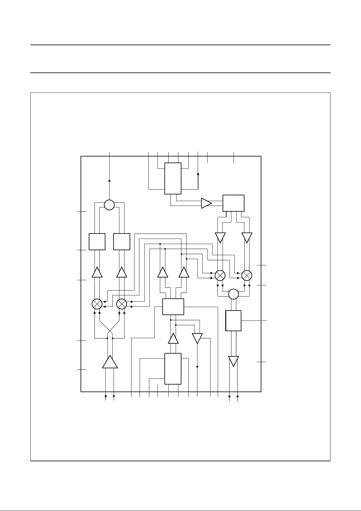
BLOCK DIAGRAM
handbook, full pagewidth
0
o
90
o
45
o
135
o
RFLO
OSCILLATOR
0
o
90
o
5
1
6
7
2
4
UAA2067
3
8
14
MGC867
11109
12
13
19
16
17
24
21
20
15
22
23
18
29
28
32 27 31
PDRX
GND6
V
CC(MIX)
V
CC1(RFLO)
V
CC2(RFLO)
V
CC(RFLOO)
GND4
GND5
RFLOA
RFLOB
RFLOREG
V
CC(TX)
GND3
GND7
RXA
RXB
TXA
TXB
PDTX TXRAMP
PDRFLO
RFLOO
V
CC(IFLO)
GND2
GND1
IFLORES
IFLOREG
PDIFLO
IFLOO
ICEN
IFDEC
IFO
30 26
25
IFLO
OSCILLATOR
LNA
RAMP
∑
∑
Fig.1 Block diagram.

1996 Oct 22 5
Philips Semiconductors Product specification
Image reject 1800 MHz transceiver
for DECT applications
UAA2067G
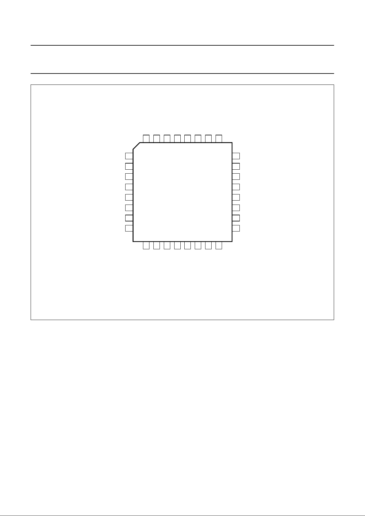
PINNING
Notes
1. Pins 3 and 7 are internally short-circuited.
2. Pins 11 and 27 should be at the same DC voltage.
3. Pins 18 and 23 are internally short-circuited.
4. Pins 19 and 22 are internally short-circuited.
SYMBOL PIN DESCRIPTION
PDIFLO 1 power-down for IFLO
IFLOREG 2 regulator decoupling for IFLO
GND1 3 ground for IFLO; note 1
IFLOO 4 IFLO output
V
CC(IFLO)
5 supply voltage for IFLO
IFLORES 6 IFLO resonator
GND2 7 ground for IFLO resonator; note 1
ICEN 8 IC enable
PDTX 9 power-down for transmitter
TXRAMP 10 power ramping transmitter
V
CC(TX)
11 supply voltage for transmitter output stage; note 2
TXB 12 transmitter RF output B
TXA 13 transmitter RF output A
GND3 14 ground for transmitter output stage
PDRFLO 15 power-down for RFLO
V
CC(RFLOO)
16 supply voltage for RFLO output
RFLOO 17 RFLO output
V
CC1(RFLO)
18 supply voltage for RFLO oscillator; note 3
GND4 19 ground for RFLO oscillator; note 4
RFLOA 20 RFLO resonator
RFLOB 21 RFLO resonator
GND5 22 ground for RFLO oscillator; note 4
V
CC2(RFLO)
23 supply voltage for RFLO oscillator; note 3
RFLOREG 24 regulator decoupling for RFLO
IFO 25 receiver IF output
IFDEC 26 IF decoupling
V
CC(MIX)
27 supply voltage for receive and transmit mixers; note 2
RXA 28 receiver RF input A
RXB 29 receiver RF input B
GND6 30 ground for receive and transmit mixers
PDRX 31 power-down for receiver
GND7 32 die-pad ground
1996 Oct 22 6
Philips Semiconductors Product specification
Image reject 1800 MHz transceiver
for DECT applications
UAA2067G
Fig.2 Pin configuration.
handbook, full pagewidth
UAA2067
MGC865
1
2
3
4
5
6
7
8
PDIFLO
IFLOREG
GND1
IFLOO
V
CC(IFLO)
IFLORES
GND2
ICEN
RFLOREG
V
CC2(RFLO)
GND5
RFLOB
RFLOA
GND4
V
CC1(RFLO)
RFLOO
24
23
22
21
20
19
18
17
9
10
11
12
13
14
15
16
PDTX
TXRAMP
V
CC(TX)
TXB
TXA
GND3
PDRFLO
V
CC(RFLOO)
32
31
30
29
28
27
26
25
GND7
PDRX
GND6
RXB
RXA
V
CC(MIX)
IFDEC
IFO

1996 Oct 22 7
Philips Semiconductors Product specification
Image reject 1800 MHz transceiver
for DECT applications
UAA2067G
FUNCTIONAL DESCRIPTION
Receive section
The circuit contains a balanced low-noise amplifier
followed by two high dynamic range mixers. The local
oscillator signals, shifted in phase to 0 and 90° mix the
amplified RF signal to the I and Q channels.These two
channels are buffered, phase shifted by 45° and 135°
respectively, amplified and recombined internally to realize
the image rejection. Signals at the RF input at RFLO − IF
frequencies are rejected through the signal processing
while signals at the RFLO + IF frequencies form the
IF signals.
An image rejection of typically 34 dB is obtained for an IF
between 100 and 120 MHz.
Balanced signals are used for minimizing crosstalk due to
package parasitics. The IF output is single-ended.
The typical load is 50 Ω.
Fast switching, on/off of the receive section is controlled
by the hardware input PDRX.
RFLO section
The high-frequency oscillator (RFLO oscillator) supplies
the local oscillator signal for the down-conversion (receive)
and up-conversion (transmit) mixers. This VCO uses an
on-chip regulator for a power-supply voltage-independent
output frequency. The buffered VCO signal is fed into a
phase shifter and an off-chip prescaler-synthesizer.
The output signal of the phase-shifter is used for driving
the RX and TX mixers. Due to the good isolation in the
buffer stages, a very small change in VCO frequency is
obtained when switching the RX and TX mixers on.
Fast switching, on/off of the oscillator section is controlled
by the hardware input PDRFLO.
IFLO section
The low-frequency oscillator (IFLO oscillator) internally
supplies the local oscillator signal to the single-sideband
transmit mixer. The buffered VCO signal is fed into a
phase shifter. The output signal of the phase-shifter is
used for driving the TX mixers.
Due to the good isolation in the buffer stages, a very small
change in VCO frequency is obtained when switching the
TX mixer on.
Fast switching on/off of the oscillator section is controlled
by the hardware input PDIFLO input.
Transmit section
The circuit contains two balanced mixers, each of which is
driven by the RFLO and IFLO signals. The output signal of
the two mixers is summed and buffered to obtain the single
upper-sideband signal at frequency RFLO + IFLO.
With the use of an off-chip time constant, the ramping
circuit defines the power ramp-up and ramp-down of the
pre-amplifier output signal.
Balanced signals are used for minimizing crosstalk due to
package parasitics.
Fast switching, on/off, of the transmit section is controlled
by the hardware input PDTX.
The power supply voltage of the transmit mixers, the
adding circuit and ramping circuit is taken from the
V
CC(MIX)
and GND6 for maximum isolation from the
preamplifier output stage.
OPERATING MODES
To use the IC, all V
CC
pins must be connected to the
supply voltage.
For transceiving a DECT signal, the RFLO and IFLO
sections should be powered-on. After a stable frequency
has been reached (mainly determined by the synthesizer
design), the receiver or transmitter can be powered-on.
GMSK data modulation can be supplied in two different
ways: the data is directly modulated on IFLO or RFLO.
The ramping of the power level can be set with a time
constant that is external to the IC.
Table 1 gives the definition of the polarity of the switching
signals on the receive, the RFLO, the IFLO and the
transmit sections.
1996 Oct 22 8
Philips Semiconductors Product specification
Image reject 1800 MHz transceiver
for DECT applications
UAA2067G
Table 1 Switching signals on the receiver
Note
1. Active when ICEN is enabled.
LIMITING VALUES
In accordance with the Absolute Maximum Rating System (IEC 134).
Note
1. Pins short-circuited internally must be short-circuited externally.
THERMAL CHARACTERISTICS
HANDLING
Every pin withstands the ESD test in accordance with
“MIL-STD-883C class 2 (method 3015.5)”
.
SIGNAL SECTION LEVEL on/off
PDRX receive section powered-on LOW on
(1)
receive section powered-off HIGH off
PDRFLO RFLO section powered-on LOW on
(1)
RFLO section powered-off HIGH off
PDIFLO IFLO section powered-on LOW on
(1)
IFLO section powered-off HIGH off
PDTX transmit section powered-on LOW on
(1)
transmit section powered-off HIGH off
ICEN all sections disabled LOW off
all sections enabled HIGH on
SYMBOL PARAMETER CONDITIONS MIN. MAX. UNIT
V
CC
supply voltage − 6V
∆GND difference in ground supply voltage applied
between all grounds
note 1 − + 0.3 V
P
l(max)
maximum power input − +20 dBm
T
j(max)
maximum operating junction temperature − +150 °C
P
dis(max)
maximum power dissipation in stagnant air at 25°C − 500 mW
T
stg
storage temperature −65 +150 °C
SYMBOL PARAMETER VALUE UNIT
R
th j-a
thermal resistance from junction to ambient in free air 90 K/W
 Loading...