

Philips UAA2062TS Datasheet

INTEGRATED CIRCUITS
DATA SH EET
UAA2062
Analog cordless telephone IC
Product specification
File under Integrated Circuits, IC17
2000 Aug 10

Philips Semiconductors Product specification
Analog cordless telephone IC UAA2062
FEATURES
RF RX (double superheterodyne FM receiver)
• Integrated Low Noise Amplifier (LNA) with
programmable gain and input impedance
• 1st mixer with external filter at 10.7 MHz
• 2nd mixer with external filter at 455 or 450 kHz
(depending on country application)
• FM detector including a fully integrated IF limiter, a
wide-band PLL and a Received Signal Strength
Indicator (RSSI) output
• Carrier Detector (CD) with programmable threshold.
RF TX
• Buffer driving an internal Power Amplifier (PA) with
programmable gain
• Narrow-band PLL including VCO
• Data transmission summing operational amplifier.
Synthesizer
• 10.24 or 11.15 MHz crystal reference oscillator (LO2)
and reference frequency divider
• Programmable TX VCO with phase detector and
frequency divider
• Programmable RX VCO (LO1)with phase detector and
frequency divider
• Programmable clock divider with output buffer to drive
the microcontroller.
Baseband RX section
• Programmable RX gain
• Expander
• Fully integrated earpiece amplifier with fixed gain.
Baseband TX section
• Microphone amplifier
• Compressor
• Programmable TX gain.
Microcontroller interface
• 3-wire serial interface.
Other features
• Voltage regulator to supply internal PLLs and the
microcontroller
• Programmable low-battery detector time multiplexed
with RSSI carrier detector.
APPLICATIONS
• World-wide analog cordless telephone set (CT0).
GENERAL DESCRIPTION
The UAA2062 is a BiCMOS integrated circuit that
performs all functions from the antenna to the
microcontroller for reception and transmission for both the
base station and the handset in a cordless telephone.
This IC integrates most of the functions required for a
cordless telephone into a single integrated circuit. The
implemented programming enables the device to be used
for the CT0 standard in many countries. Additionally, the
implemented programming significantly reduces the
amount of external components, board space
requirements and external adjustments.
ORDERING INFORMATION
TYPE NUMBER
NAME DESCRIPTION VERSION
UAA2062TS SSOP48 plastic shrink small outline package; 48 leads; body width 7.5 mm SOT370-1
2000 Aug 10 2
PACKAGE
Philips Semiconductors Product specification
Analog cordless telephone IC UAA2062
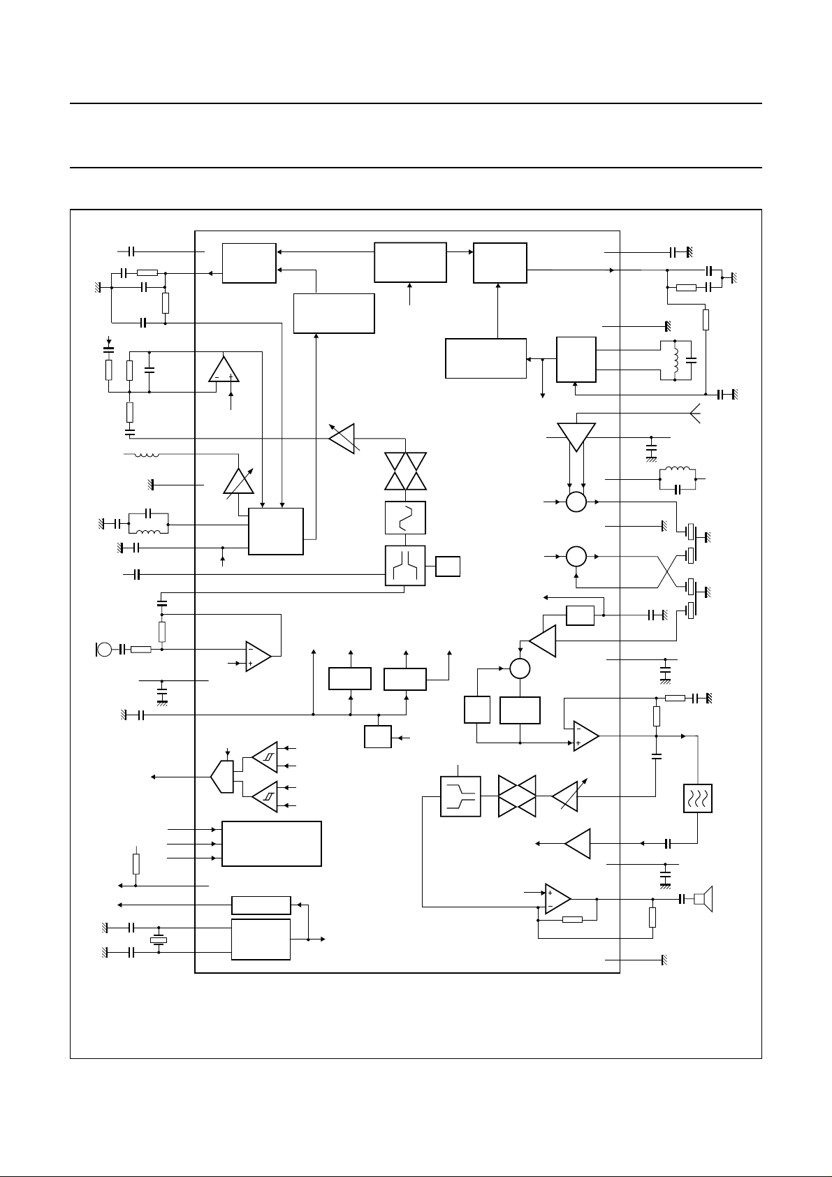
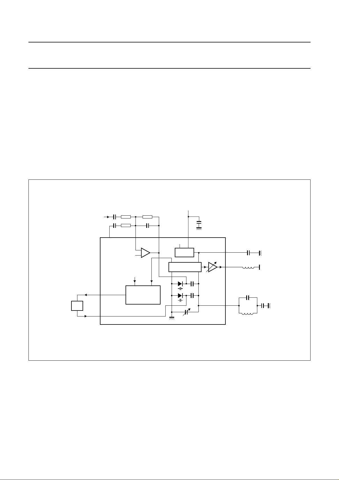
BLOCK DIAGRAM
handbook, full pagewidth
V
CC
data TX
V
CC
V
CC
V
CC(AUTX)
V
CC
220 kΩ
(1)
crystal
ECAP 1
TXPD 2
TXLF 3
MODO 4
MODI 5
TXO 6
PAO 7
TXGND
LO3I
V
REFTX
CCAP
CMPI
MICO
MICI
VB
CDBDO
EN
DATA 19
CLK
DATO
CLKO
LO2O
LO2I
TX PHASE
DETECTOR
VBMOD
PA
8
9
10
V
REFTX
11
12
13
microphone
amplifier
14
VB
15
16
CD/BD
17
18
MICROCONTROLLER
20
21
22
23
24
CRYSTAL
OSCILLATOR
TX VCO
LBD
CD
SERIAL
INTERFACE
DIVIDER
14-BIT TX
PROGRAMMABLE
DIVIDER
TX gain
CCAP
V
ref(PLL)
VB
REG 3 V
VB
V
CC
VB
RSSI
VB
LO2
REFERENCE
DIVIDER
(2048 or 892)
V
REFTX
REG 3 V
V
ref
LO2
TX mute
compressor
VB
V
CC(AU)
14-BIT RX
PROGRAMMABLE
DIVIDER
hard
limiter
ALC
UAA2062
VBMOD
VCO
ECAP
expander
RX PHASE
DETECTOR
LOOP
FILTER
RX mute
DATO
VB
×
BPFI
LO1
LO2
RSSI
LO1
LIM
data
amplifier
earpiece
amplifier
RX
VCO
LNA
1st mixer
2nd mixer
RSSI
amplifier
RX gain
V
ref(PLL)
48
47
RXPD
PLLGND
46
LO1O
45
LO1I
44
RXLF
43
RFI
42
V
CC(LNA)
41
BPFI
40
MX1O
39
×
RFGND
38
MX2O
37
×
MX2I36
RSSI
35
LIMI34
V
CC(RF)
33
PLLO32
DETO
31
RXI
30
DATI
29
V
CC(AU)
28
EARO
27
EARI
26
AUGND
25
RF
V
1st IF filter
2nd IF filter
CC
(1)
(1)
(1) Values are depending on country application (see definition in Chapter “Channel frequencies”).
Fig.1 Block diagram.
2000 Aug 10 3
FCA120
Philips Semiconductors Product specification
Analog cordless telephone IC UAA2062
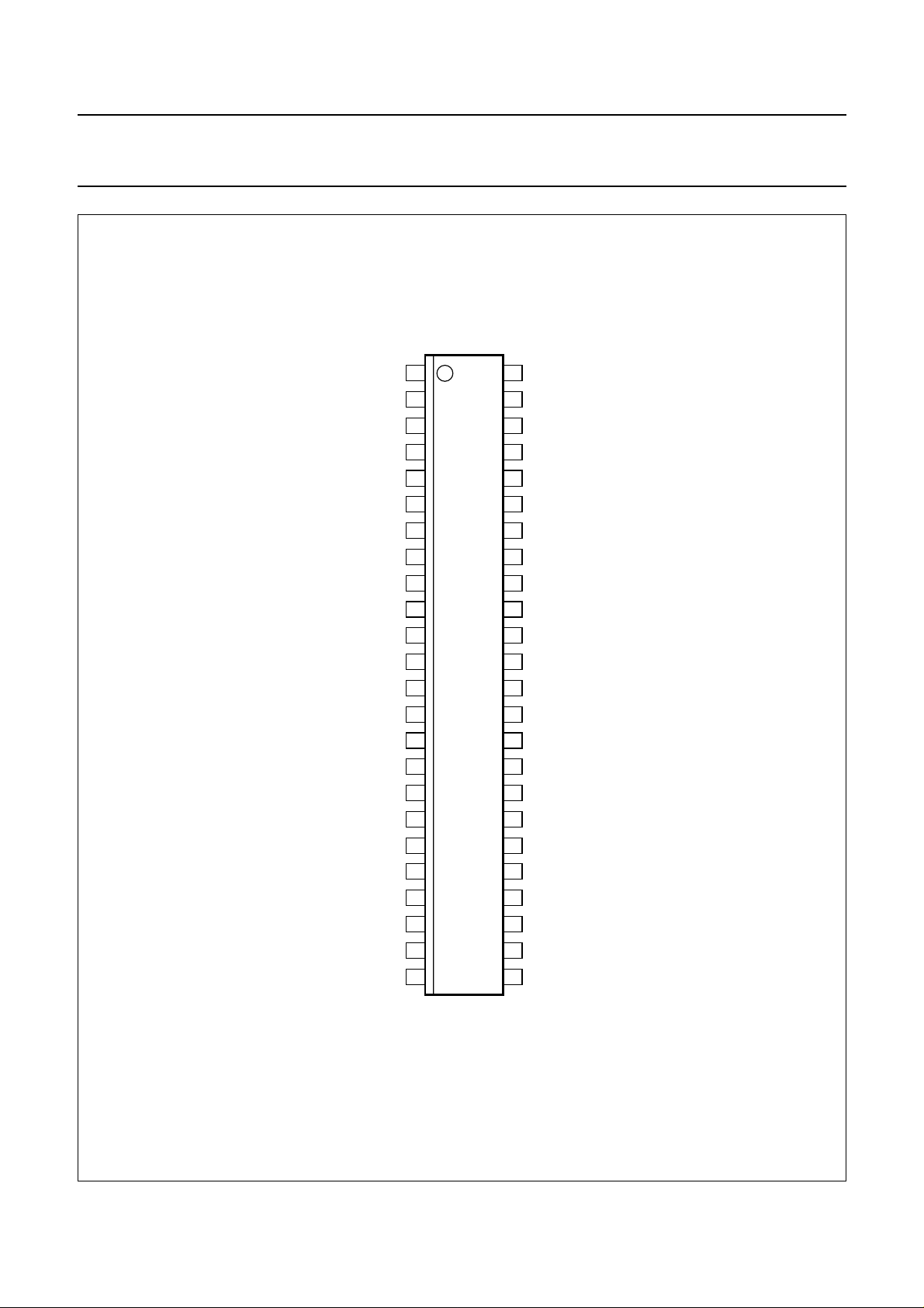
PINNING
SYMBOL PIN DESCRIPTION
ECAP 1 output pin for external capacitor
from expander
TXPD 2 phase detector output voltage for
TX PLL
TXLF 3 input from loop filter to TX VCO
MODO 4 summing amplifier output voltage
MODI 5 summing amplifier inverting input
TXO 6 TX baseband output voltage
PAO 7 power amplifier output
TXGND 8 ground for RF TX chain and PA
LO3I 9 TX VCO input
V
REFTX
10 output pin for decoupling
capacitorforregulatedvoltagefor
TX VCO
CCAP 11 output pin for external capacitor
from compressor
CMPI 12 compressor input voltage
MICO 13 microphone amplifier output
voltage
MICI 14 microphone amplifier inverting
input
V
CC(AUTX)
15 supply voltage for TX audio
VB 16 internal voltage reference
CDBDO 17 multiplexed output from carrier
detector or low-battery detector
EN 18 enable signal for serial interface
DATA 19 data signal for serial interface
CLK 20 clock signal for serial interface
DATO 21 data comparator output
CLKO 22 output pin for external clock
LO2O 23 crystal oscillator output
SYMBOL PIN DESCRIPTION
LO2I 24 crystal oscillator input
AUGND 25 ground for audio part
EARI 26 earpiece amplifier inverting input
EARO 27 earpiece amplifier output voltage
V
CC(AU)
28 supply voltage for audio part
DATI 29 data comparator input
RXI 30 RX audio input voltage
DETO 31 amplifier FM PLL output voltage
PLLO 32 amplifier FM PLL inverting input
V
CC(RF)
33 supply voltage for RF RX
LIMI 34 limiter input voltage
RSSI 35 output pin for external capacitor
from RSSI
MX2I 36 2nd mixer input
MX2O 37 2nd mixer output
RFGND 38 ground for RF RX
MX1O 39 1st mixer output voltage
BPFI 40 LNA output for external LC
V
CC(LNA)
41 supply voltage for LNA
RFI 42 LNA input voltage
RXLF 43 input from loop filter to RX VCO
LO1I 44 input pin to connect the
external LC for RX VCO
LO1O 45 output pin to connect the
external LC for RX VCO
PLLGND 46 ground for digital part of the PLL
RXPD 47 phase detector output voltage for
RX PLL
V
ref(PLL)
48 output pin for decoupling
capacitorforregulatedvoltagefor
internal PLLs and microcontroller
2000 Aug 10 4
Philips Semiconductors Product specification
Analog cordless telephone IC UAA2062
handbook, halfpage
V
CC(AUTX)
ECAP
TXPD
TXLF
MODO
MODI
TXO
PAO
TXGND
LO3I
V
REFTX
CCAP
CMPI
MICO
MICI
CDBDO
DATA
CLK
DATO
CLKO
LO2O
LO2I
VB
EN
1
2
3
4
5
6
7
8
9
10
11
12
13
14
15
16
17
18
19
20
21
22
23
24
UAA2062
FCA091
48
47
46
45
44
43
42
41
40
39
38
37
36
35
34
33
32
31
30
29
28
27
26
25
V
ref(PLL)
RXPD
PLLGND
LO1O
LO1I
RXLF
RFI
V
CC(LNA)
BPFI
MX1O
RFGND
MX2O
MX2I
RSSI
LIMI
V
CC(RF)
PLLO
DETO
RXI
DATI
V
CC(AU)
EARO
EARI
AUGND
Fig.2 Pin configuration.
2000 Aug 10 5
Philips Semiconductors Product specification
Analog cordless telephone IC UAA2062
FUNCTIONAL DESCRIPTION
Power supply and power management
1. In the active mode all blocks are powered.
2. In the RX mode, all circuitry in the receiver part is
powered.
POWER SUPPLY VOLTAGE
TheUAA2062is used in a cordless telephone handsetand
inabaseunit.The handset unit is battery poweredandcan
operateonthreeNiCadcells.Theminimumsupply voltage
(VCC) is 3.0 V. However the low-battery detector, crystal
oscillator, clock divider and internal voltage regulator will
function with a supply voltage of 2.85 V.
3. In the standby mode, all circuitry is powered down
except the crystal oscillator, the microcontroller
interface and the V
ref(PLL)
block.
4. In the inactive mode, all circuitry is powered down
except the microcontroller interface and the V
ref(PLL)
block.
Latch memory is maintained in all modes. Table 1 shows
POWER SAVING OPERATION MODES
which blocks are powered in each mode.
When the UAA2062is used in a handset, it is important to
reducethecurrentconsumption.There are 3 powersaving
modes in addition to the active mode:
Table 1 Power saving operation modes
CIRCUIT BLOCK
ACTIVE
MODE
RX MODE
STANDBY
MODE
INACTIVE
MODE
Microcontroller interface XXXX
V
ref(PLL)
XXX
(1)
(1)
X
Crystal oscillator X X X −
RF receiver and RX PLL X X −−
VB reference X X −−
Carrier and low-battery detectors X X −−
Data comparator X X −−
TX PLL and PA X −−−
RX and TX audio paths X −−−
Note
1. In the standby mode and in the inactive mode, by default, V
(bit V
disable is logic 0). If bit V
REFPLL
disable is logic 1, V
REFPLL
remains regulated but is not calibrated
ref(PLL)
is not regulated and fluctuates with VCC.
ref(PLL)
MAXIMUM CURRENT CONSUMPTION
Table 2 shows the typical and the maximum current consumption in the active mode and the three current saving modes
under the followingconditions:IP3HIGHmode (bit IP3 is logic 1), see Table 6; LNA gain is step 3 (bits LNA are logic 11),
see Table 12 and the PA output level is step 3 (bits PA are logic 11), see Table15.
In the standby mode and in the inactive mode, pin V
is not powered (bit V
ref(PLL)
disable is logic 1) and the clock
REFPLL
output signal is disabled (bits clock divider ratio are logic 00).
2000 Aug 10 6

Philips Semiconductors Product specification
Analog cordless telephone IC UAA2062
Table 2 Current consumption in the 4 operating modes (VCC= 3.6 V; T
=25°C); see Table 5 for programming of
amb
the power saving operation modes
POWER OPERATING MODE
TYPICAL CURRENT
CONSUMPTION (mA)
MAXIMUM CURRENT
CONSUMPTION (mA)
active mode 27 36
RX mode 11 15
standby mode 0.35 0.5
inactive mode 0.05 0.1
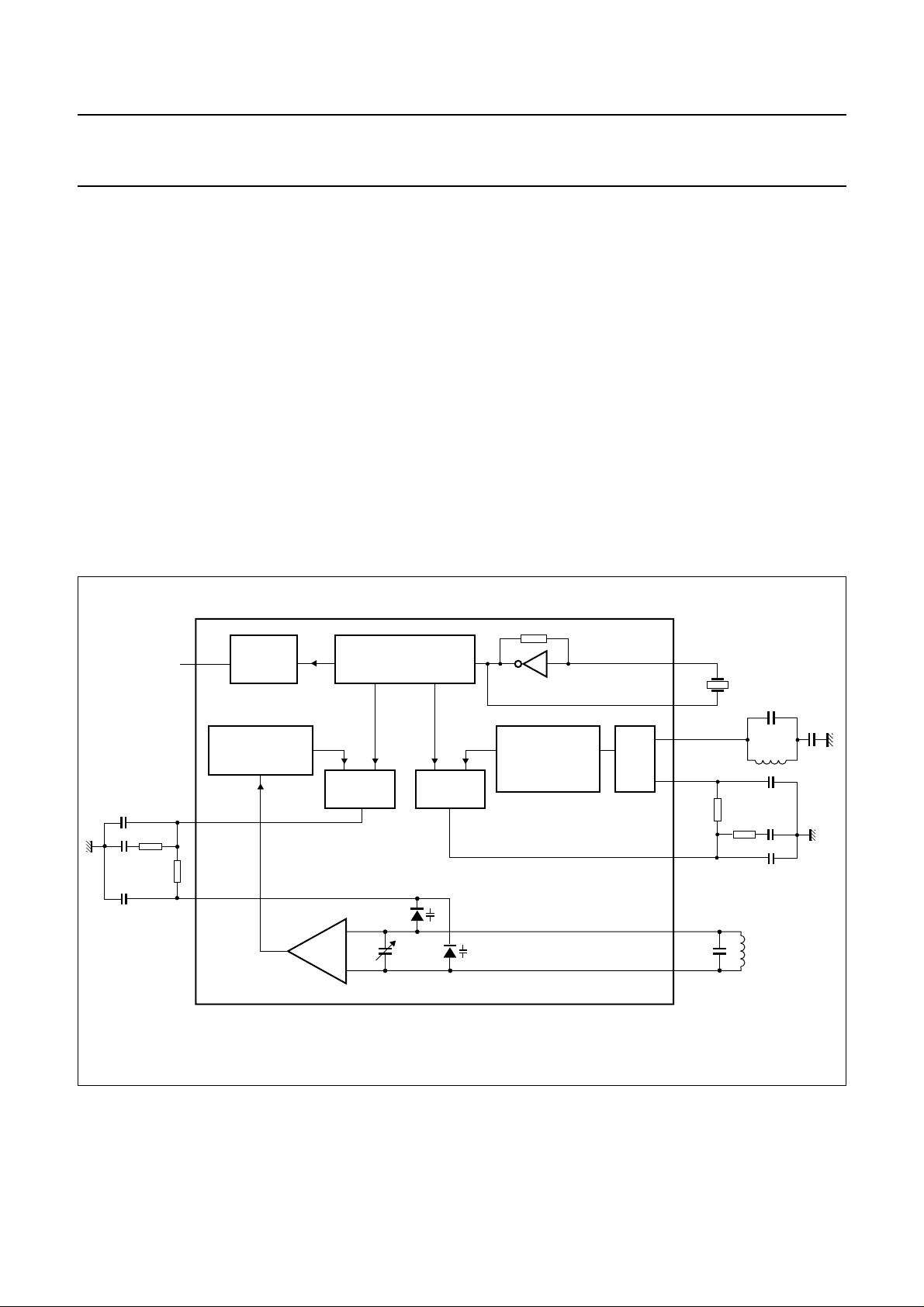
The FM receiver part
FM
RECEIVER
The FM receiver has the programmability to operate for all country channels, including the 25 U.S. channels, without the
need for external switching circuitry (see Fig.3).
The gain and input impedance of the LNA are programmable. The LNA also includes a programmable capacitance to
avoid external manual fine tuning.
handbook, full pagewidth
RF
1st IF filter
(1)
2nd IF filter
(1)
RFI
42
LNA
DUAL PLL
FREQUENCY
SYNTHESIZER
47
RXPD43RXLF45LO1O44LO1I
LPF
(1) Values depend on the country application (see definition in Chapter “Channel frequencies”).
BPFI
40
MX1O
39
MX2I
36
MX2O34LIMI
37
IF limiter
× × ×
1st mixer 2nd mixer
RSSI
RX VCO
CRYSTAL
OSCILLATOR
24
LO2I23LO2O35RSSI
crystal
(1)
Fig.3 FM receiver schematic diagram.
PLLO31DETO
32
LOOP
FILTER
VCO
V
ref
amplifier
carrier
detect output
FCA121
2000 Aug 10 7
Philips Semiconductors Product specification
Analog cordless telephone IC UAA2062
DATA COMPARATOR
The data comparator is an inverting hysteresis
comparator. An external filter is connected between
pins DETO and DATI (AC-coupled). The open-collector
output is current limited to control the output signal slew
rate. The external resistor at pin DATO, connected to VCC,
should be 220 kΩ. An external capacitor in parallel with
this resistor will reduce the slew rate.
The transmit part
The transmitter architecture is of the direct modulation
type. The transmit VCO can be frequency modulated
either by speech or data (see Fig.4).
handbook, full pagewidth
data TX
TXO
MODI5MODO
6
VBMOD
summing
amplifier
10.24 MHz
TRANSMIT VCO
Before the VCO, an amplifier sums the modulating signal
and the data TX signal. The Colpitts type transmit VCO
includesintegratedvaricaps.Fixedexternal capacitors are
used to extend the tuning range for all countries.
The internal capacitors are programmed via the serial bus
interface. The power amplifier is capable of driving
50 Ω AC. The output level is also programmed with 2 bits
via the serial bus interface. An internal regulator supplies
the TX VCO.
V
CC(AUTX)
VB
REG 3 V
TX VCO
15
V
10
REFTX
PAO
7
PA
4
2TXPD
LPF
3TXLF
DUAL PLL
FREQUENCY
SYNTHESIZER
Fig.4 Transmit schematic diagram.
2000 Aug 10 8
9 LO3I
FCA122
Philips Semiconductors Product specification
Analog cordless telephone IC UAA2062
The synthesizer
The synthesizer has been designed to support most
country channel frequencies between 25 and 50 MHz
(see Chapter “Channel frequencies”).
The local oscillator LO2 and the reference divider provide
the reference frequency for the RX and TX PLL loops.
A singlebitprogrammesthedividervaluefor the reference
divider. A 5 kHz reference frequency (respectively
12.5 kHz) is used with a 10.24 MHz crystal frequency
(respectively 11.15 MHz). The clock divider ratio can be
programmed to 2.5 or to 80. The ratio 80 can be chosen
whenthe IC is in sleep modetoobtaincurrentsavinginthe
microcontroller. The clock output is a CMOS output
inverter, supplied by V
ref(PLL)
.
The 14-bit TX counter is programmed for the desired
transmit channel frequency. The 14-bit RX counter is
programmed for the desired RX VCO frequency.
ndbook, full pagewidth
CLOCK
22CLKO
DIVIDER
1-BIT PROGRAMMABLE
REFERENCE COUNTER
/2048 or /892
All counters power-up in the proper default state and for a
10.24 MHz reference crystal. Both RX and TX phase
detectors have current drive type outputs of 400 µA.
The RX VCO is connected to an external capacitor and
inductor as illustrated in Fig.5. The varicaps are integrated.
Operating in the 25 US channels, there is a large
frequency difference between the minimum and the
maximum channel frequencies. The sensitivity of the
RX VCO is not large enough to accommodate this large
frequency range. Internal programmable capacitors can
be connected across the RX VCO tank circuit to change
the RX VCO sensitivity. The TX VCO also has internal
programmable capacitors to accommodate a large
frequency range. Chapter “Channel frequencies” shows
the frequency selection for all countries.
24
LO2I
crystal oscillator
23
LO2O
C1
C2
C3
R2
R3
RXLF
14-BIT
PROGRAMMABLE
RX COUNTER
47RXPD
43
PROGRAMMABLE
RX PHASE
DETECTOR
RX VCO
TX PHASE
DETECTOR
Fig.5 Synthesizer schematic diagram.
14-BIT
TX COUNTER
TX
VCO
9 LO3I
3
2 TXPD
44 LO1I
45 LO1O
FCA123
TXLF
R6
R5
C6
C5
C4
2000 Aug 10 9
Philips Semiconductors Product specification
Analog cordless telephone IC UAA2062
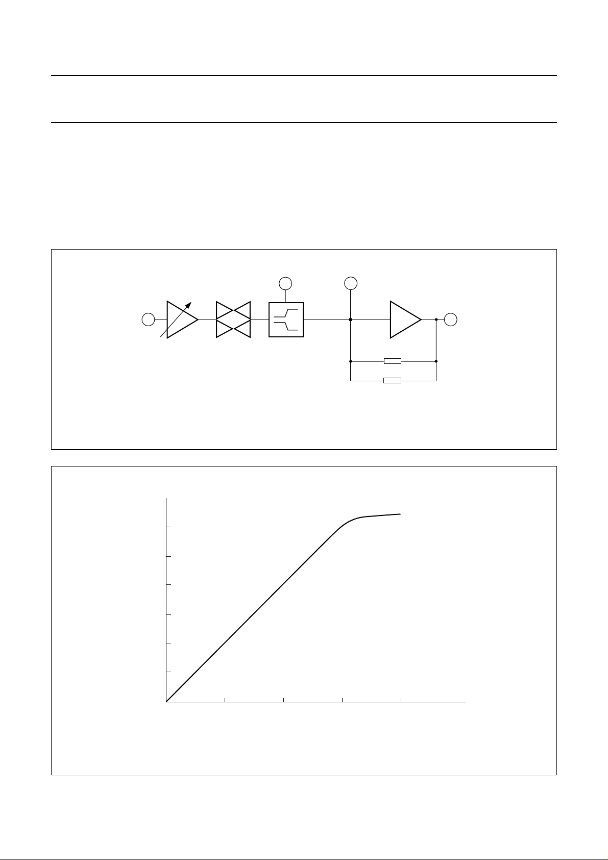
The RX baseband
This section covers the RX audio path from pins RXI to
EARO. The RXI input signal is AC-coupled.
The microcontroller sets the value of the RX gain by
32 linear steps of 0.5 dB. The RX baseband has a mute
and an expander with the characteristics shown in Fig.7.
handbook, full pagewidth
RXI
30
RX gain
RX mute
ECAP
expander
Fig.6 RX baseband schematic diagram.
EARPIECE AMPLIFIER
The earpiece amplifier is an inverting rail-to-rail
operational amplifier. The non-inverting input is connected
to the internal reference voltage VB. Internal resistors are
used to set the gain at 6 dB. An external resistor
(connected between pins EARI and EARO) can be used
to reduce the gain.
EARI
1
26
earpiece amplifier
EARO
27
internal resistor : 28 kΩ
external resistor
FCA124
handbook, full pagewidth
(1) ∆G
ARX
= 0 dB, G
EARO
(dBV)
0
−10
−20
−30
−40
−50
−60
−40 −30
= 0 dB (external resistor of 28 kΩ).
EAR
−40
−20
−20 −10 0
Fig.7 Expander characteristic.
2000 Aug 10 10
FCA127
EARO = −7 dBV typical at THD = 5%
RXI (dBV)
Philips Semiconductors Product specification
Analog cordless telephone IC UAA2062
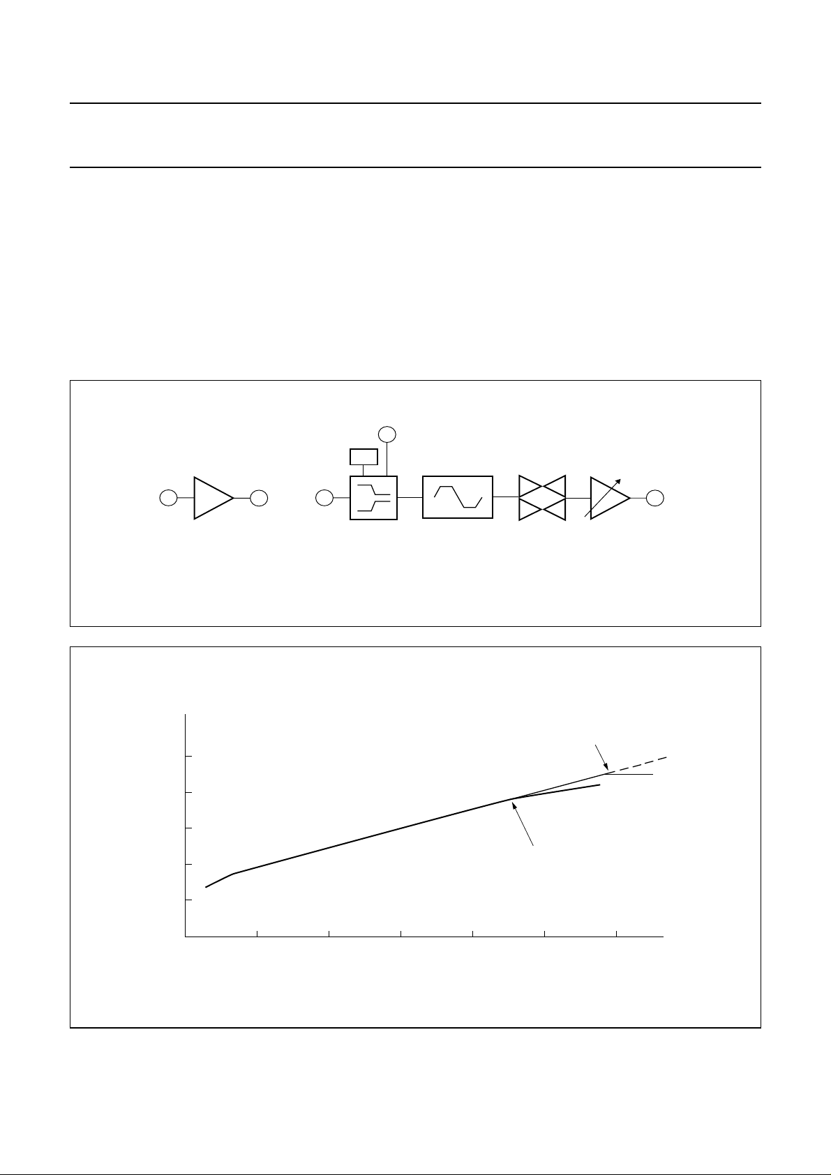
The TX baseband
This section covers the TX audio path from pins MICI to
TXO.
The microphone amplifier is an inverting operational
amplifier whose gain can be set by external resistors. The
input signal at pin MICI and the output signal at pin MOCO
arebothAC-coupled.Thenon-invertinginputisconnected
to the internal reference voltage VB. External resistors are
used to set the gain and frequency response.
handbook, full pagewidth
MICI
14
microphone
amplifier
MICO
13
CMPI
12
CCAP
11
ALC
The TX baseband has a compressor with the
characteristicshowninFig.9. The Automatic Level Control
(ALC) provides a ‘soft’ limit to the output signal swing as
the input voltage increases slowly (i.e. a sine wave is
maintained at the output). A hard limiter clamps the
compressor output voltage at 1.26 V (p-p). The ALC and
the hard limiter can be disabled via the microcontroller
interface. The hard limiter is followed by a mute circuit.
The TX gain is digitally programmable in 32 steps of
0.5 dB.
TXO
6
hard limiter
TX mutecompressor
TX gain
FCA125
handbook, full pagewidth
TXO
(dBV)
0
−10
−20
−30
−40
−60 −50
−30
Fig.8 TX baseband schematic diagram.
V
= −4 dBV; V
CMPI
(hard limiting signals)
−20
V
CMPI
−40 −30 −20 −10 0
= −1.26 V(p-p)
TXO
V
CMPI
V
= −11.5 dBV
TXO
= −16 dBV; V
(slowly changing ALC signals)
CMPI (dBV)
Fig.9 Compressor characteristic.
= −2.5 dBV
TXO
= −13 dBV
FCA126
2000 Aug 10 11
Philips Semiconductors Product specification
Analog cordless telephone IC UAA2062
Other features
PLL VOLTAGE REGULATOR
Pin V
RX and TX PLLs. It is regulated at 3 V. Pin V
provides the internal supply voltage for the
ref(PLL)
CC(AU)
provides the supply voltage input for the internal voltage
regulator. Two capacitors of 47 µF and 100 nF must be
connected to pin V
to filter and stabilize this
ref(PLL)
regulated voltage. The tolerance of the regulated voltage
is initially ±8% but is improved to ±4% after the internal
band gap voltage reference is adjusted via the
microcontroller.
The voltage regulator is always turned on. In the inactive
mode the calibration is turned off to reduce current
consumption. In this mode, the V
block supplies
ref(PLL)
300 µA to the microcontroller. The output drive capability
is 3 mA. The voltage regulator is able to supply the
microcontroller.
The local oscillator LO2 and the RX and TX phase
detectors are powered by the internal voltage regulator at
pin V
. Therefore, the maximum input and output
ref(PLL)
level for most I/O pins (LO2I and LO2O) equals the
regulated voltage at pin V
ref(PLL)
.
The comparator has a built-in hysteresis to prevent
spuriousswitching.Theprecision of thedetectiondepends
on the divider accuracy, the comparator offset and the
accuracy of the reference voltage VB. The output is
multiplexed at pin CDBDO. When the battery voltage level
is below the threshold voltage the output CDBDO is going
LOW.
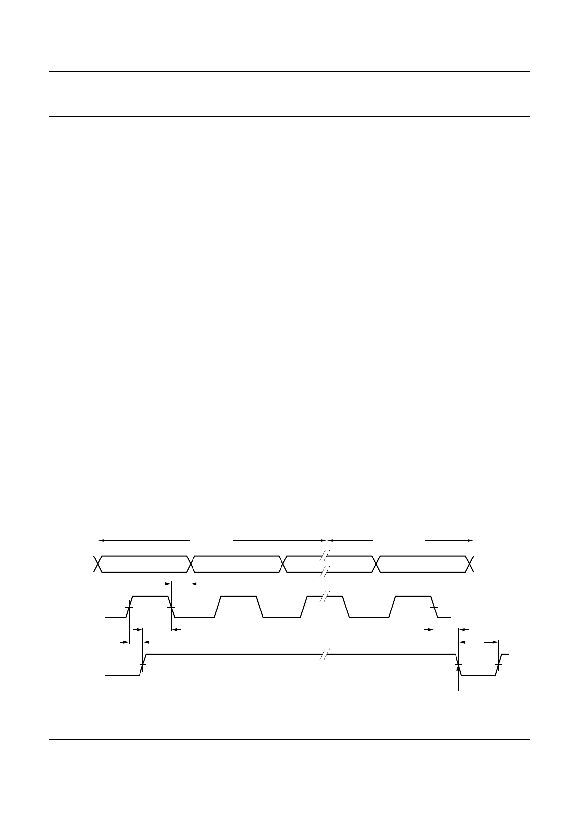
Microcontroller serial interface
Pins DATA, CLK and EN provide a 3-wire unidirectional
serial interface for programming the reference counters,
the transmit and receive channel divider counters and the
control functions.
Theinterfaceconsists of 18-bit shift registers connected to
a matrix of registers organized as 6 words of 18 bits. The
leading 15 bits include the data D14 to D0. The trailing
3 bits set up the address AD2 to AD0. The data is entered
with the most significant bit D14 first. The last bit is
bit AD0.
Pins DATA and CLK are used to load data into the shift
register. Figure 10 shows the timing required on all pins.
Data is clocked into the shift registers on negative clock
transitions.
LOW-BATTERY DETECTOR
The low-battery detector measures the voltage level of the
V
using a resistance divider and a comparator. One
CC(AU)
inputofthecomparatoris connected to VB,theothertothe
middle point of the resistance divider.
handbook, full pagewidth
DATA
CLK
EN
D14 D13 D12 AD1 AD0
50%
t
HD;EC
t
SU;CE
50%
data bits (15) address bits (3)
t
SU;DC
50%
The serial interface pins DATA, CLK and EN, are supplied
by V
. Internal level shifters are provided after the
ref(PLL)
pins which allow the logic and registers to be internally
powered by V
CC(AU)
.
TheESD protection diodes on these pins are connected to
V
. All the digital outputs (CDBDO and DATO) are
CC(AU)
open-collector outputs.
t
END
t
w
data bits latched
MGR004
Fig.10 Digital signals timing requirement.
2000 Aug 10 12
 Loading...