

Philips UA741CN, UA741CD, UA741CNB, UA741N Datasheet
Philips Semiconductors Product specification
µA741/µA741C/SA741CGeneral purpose operational amplifier
1
1994 Aug 31 853-0903 13721
DESCRIPTION
The µA741 is a high performance operational amplifier with high
open-loop gain, internal compensation, high common mode range
and exceptional temperature stability. The µA741 is
short-circuit-protected and allows for nulling of offset voltage.
FEATURES
•Internal frequency compensation
•Short circuit protection
•Excellent temperature stability
•High input voltage range
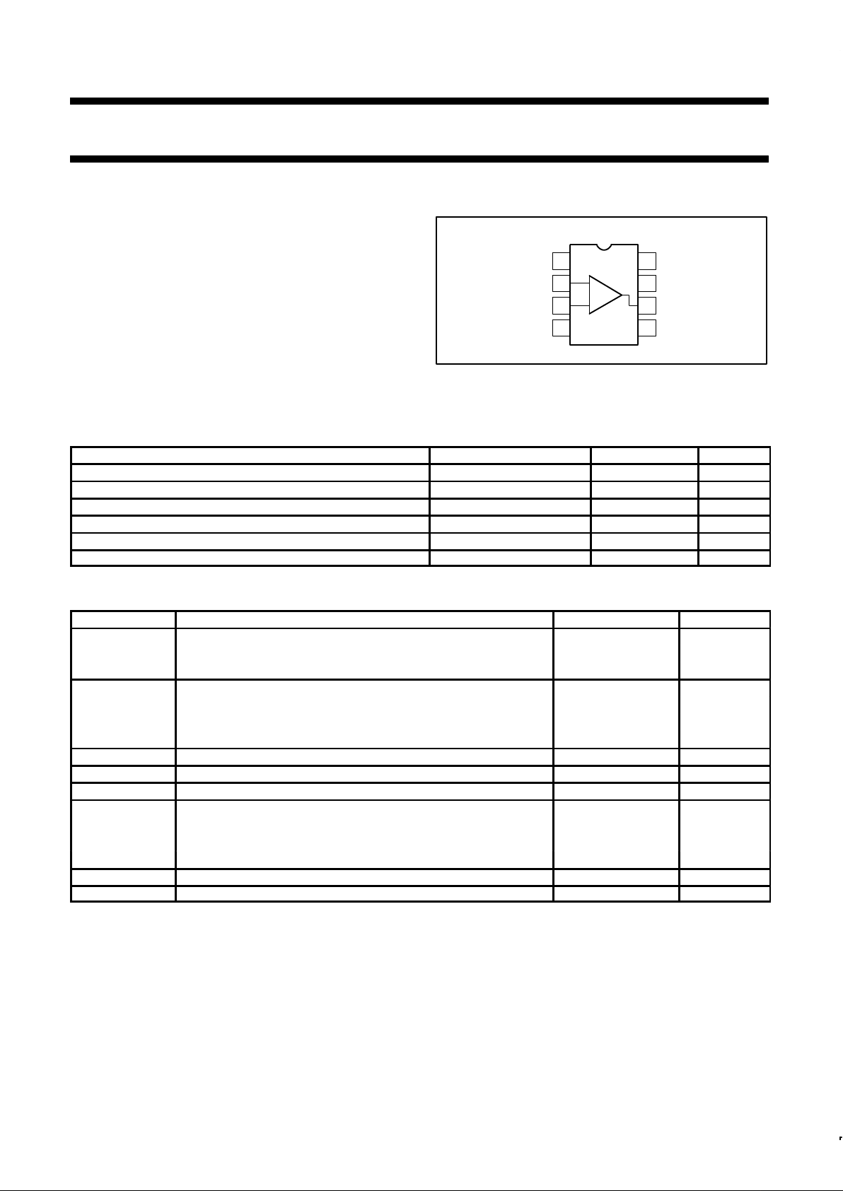
PIN CONFIGURATION
1
2
3
4 5
6
7
8
–
+
OFFSET NULL
INVERTING INPUT
NON–INVERTING INPUT
V –
NC
V +
OUTPUT
OFFSET NULL
TOP VIEW
D, F, N Packages
SL00095
Figure 1. Pin Configuration
ORDERING INFORMATION
DESCRIPTION TEMPERATURE RANGE ORDER CODE DWG #
8-Pin Plastic Dual In-Line Package (DIP) -55°C to +125°C µA741N SOT97-1
8-Pin Plastic Dual In-Line Package (DIP) 0 to +70°C µA741CN SOT97-1
8-Pin Plastic Dual In-Line Package (DIP) -40°C to +85°C SA741CN SOT97-1
8-Pin Ceramic Dual In-Line Package (CERDIP) -55°C to +125°C µA741F 0580A
8-Pin Ceramic Dual In-Line Package (CERDIP) 0 to +70°C µA741CF 0580A
8-Pin Small Outline (SO) Package 0 to +70°C µA741CD SOT96-1
ABSOLUTE MAXIMUM RATINGS
SYMBOL PARAMETER RATING UNIT
V
S
Supply voltage
µA741C ±18 V
µA741 ±22 V
P
D
Internal power dissipation
D package 780 mW
N package 1170 mW
F package 800 mW
V
IN
Differential input voltage ±30 V
V
IN
Input voltage
1
±15 V
I
SC
Output short-circuit duration Continuous
T
A
Operating temperature range
µA741C 0 to +70 °C
SA741C -40 to +85 °C
µA741 -55 to +125 °C
T
STG
Storage temperature range -65 to +150 °C
T
SOLD
Lead soldering temperature (10sec max) 300 °C
NOTES:
1. For supply voltages less than ±15V, the absolute maximum input voltage is equal to the supply voltage.
Philips Semiconductors Product specification
µA741/µA741C/SA741CGeneral purpose operational amplifier
1994 Aug 31
2
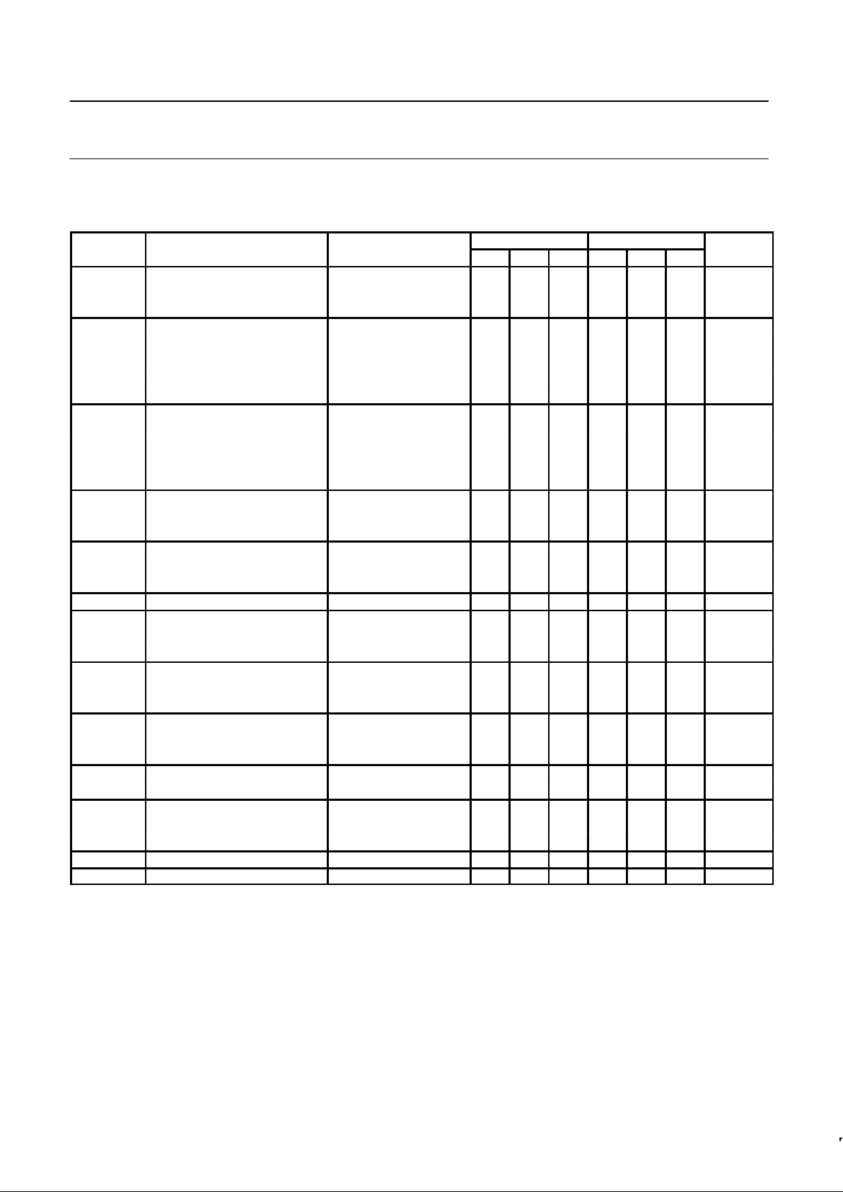
DC ELECTRICAL CHARACTERISTICS
T
A
= 25°C, V
S
= ±15V, unless otherwise specified.
µA741 µA741C
SYMBOL
PARAMETER
TEST CONDITIONS
Min Typ Max Min Typ Max
UNIT
V
OS
Offset voltage RS=10kΩ 1.0 5.0 2.0 6.0 mV
RS=10kΩ, over temp. 1.0 6.0 7.5 mV
∆VOS/∆T 10 10 µV/°C
I
OS
Offset current 20 200 20 200 nA
Over temp. 300 nA
TA=+125°C 7.0 200 nA
TA=-55°C 20 500 nA
∆IOS/∆T 200 200 pA/°C
I
BIAS
Input bias current 80 500 80 500 nA
Over temp. 800 nA
TA=+125°C 30 500 nA
TA=-55°C 300 1500 nA
∆IB/∆T 1 1 nA/°C
RL=10kΩ ±12 ±14 ±12 ±14 V
V
OUT
Output voltage swing
RL=2kΩ, over temp. ±10 ±13 ±10 ±13 V
RL=2kΩ, VO=±10V 50 200 20 200 V/mV
A
VOL
Large-signal voltage gain RL=2kΩ, VO=±10V,
over temp. 25 15 V/mV
Offset voltage adjustment range ±30 ±30 mV
RS≤10kΩ 10 150 µV/V
PSRR Supply voltage rejection ratio
RS≤10kΩ, over temp. 10 150 µV/V
70 90 dB
CMRR Common-mode rejection ratio
Over temp. 70 90 dB
1.4 2.8 1.4 2.8 mA
I
CC
Supply current TA=+125°C 1.5 2.5 mA
TA=-55°C 2.0 3.3 mA
V
IN
Input voltage range (µA741, over temp.) ±12 ±13 ±12 ±13 V
R
IN
Input resistance 0.3 2.0 0.3 2.0 MΩ
50 85 50 85 mW
P
D
Power consumption TA=+125°C 45 75 mW
TA=-55°C 45 100 mW
R
OUT
Output resistance 75 75 Ω
I
SC
Output short-circuit current 10 25 60 10 25 60 mA
Philips Semiconductors Product specification
µA741/µA741C/SA741CGeneral purpose operational amplifier
1994 Aug 31
3
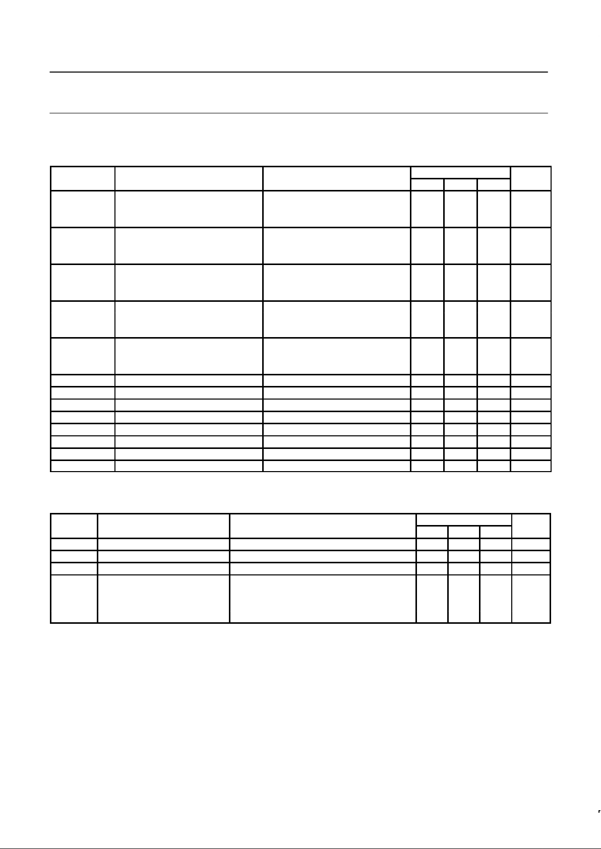
DC ELECTRICAL CHARACTERISTICS
T
A
= 25°C, V
S
= ±15V, unless otherwise specified.
SA741C
SYMBOL
PARAMETER
TEST CONDITIONS
Min Typ Max
UNIT
V
OS
RS=10kΩ 2.0 6.0 mV
Offset voltage RS=10kΩ, over temp. 7.5 mV
∆VOS/∆T 10 µV/°C
I
OS
20 200 nA
Offset current Over temp. 500 nA
∆IOS/∆T 200 pA/°C
I
BIAS
80 500 nA
Input bias current Over temp. 1500 nA
∆IB/∆T 1 nA/°C
RL=10kΩ ±12 ±14 V
V
OUT
Output voltage swing
RL=2kΩ, over temp. ±10 ±13 V
RL=2kΩ, VO=±10V 20 200 V/mV
A
VOL
Large-signal voltage gain
RL=2kΩ, VO=±10V, over temp. 15 V/mV
Offset voltage adjustment range ±30 mV
PSRR Supply voltage rejection ratio RS≤10kΩ 10 150 µV/V
CMRR Common mode rejection ration 70 90 dB
V
IN
Input voltage range Over temp. ±12 ±13 V
R
IN
Input resistance 0.3 2.0 MΩ
P
d
Power consumption 50 85 mW
R
OUT
Output resistance 75 Ω
I
SC
Output short-circuit current 25 mA
AC ELECTRICAL CHARACTERISTICS
TA=25°C, V
S
= ±15V, unless otherwise specified.
µA741, µA741C
SYMBOL
PARAMETER
TEST CONDITIONS
Min Typ Max
UNIT
R
IN
Parallel input resistance Open-loop, f=20Hz 0.3 MΩ
C
IN
Parallel input capacitance Open-loop, f=20Hz 1.4 pF
Unity gain crossover frequency Open-loop 1.0 MHz
Transient response unity gain VIN=20mV, RL=2kΩ, CL≤100pF
t
R
Rise time 0.3 µs
Overshoot 5.0 %
SR Slew rate C≤100pF, RL≥2kΩ, VIN=±10V 0.5 V/µs
 Loading...