

Philips ua733 DATASHEETS
LINEAR PRODUCTS
µA733/733C
Differential video amplifier
Product specification April 15, 1992
IC11
Philips Semiconductors
Philips Semiconductors Product specification
µA733/733CDifferential video amplifier
DESCRIPTION
The 733 is a monolithic differential input, differential output,
wide-band video amplifier. It offers fixed gains of 10, 100, or 400
without external components, and adjustable gains from 10 to 400
by the use of an external resistor. No external frequency
compensation components are required for any gain option. Gain
stability, wide bandwidth, and low phase distortion are obtained
through use of the classic series-shunt feedback from the
emitter-follower outputs to the inputs of the second stage. The
emitter-follower outputs provide low output impedance, and enable
the device to drive capacitive loads. The 733 is intended for use as
a high-performance video and pulse amplifier in communications,
magnetic memories, display and video recorder systems.
FEA TURES
•120MHz bandwidth
•250kΩ input resistance
•Selectable gains of 10, 100, and 400
•No frequency compensation required
•MIL-STD-883A, B, C available
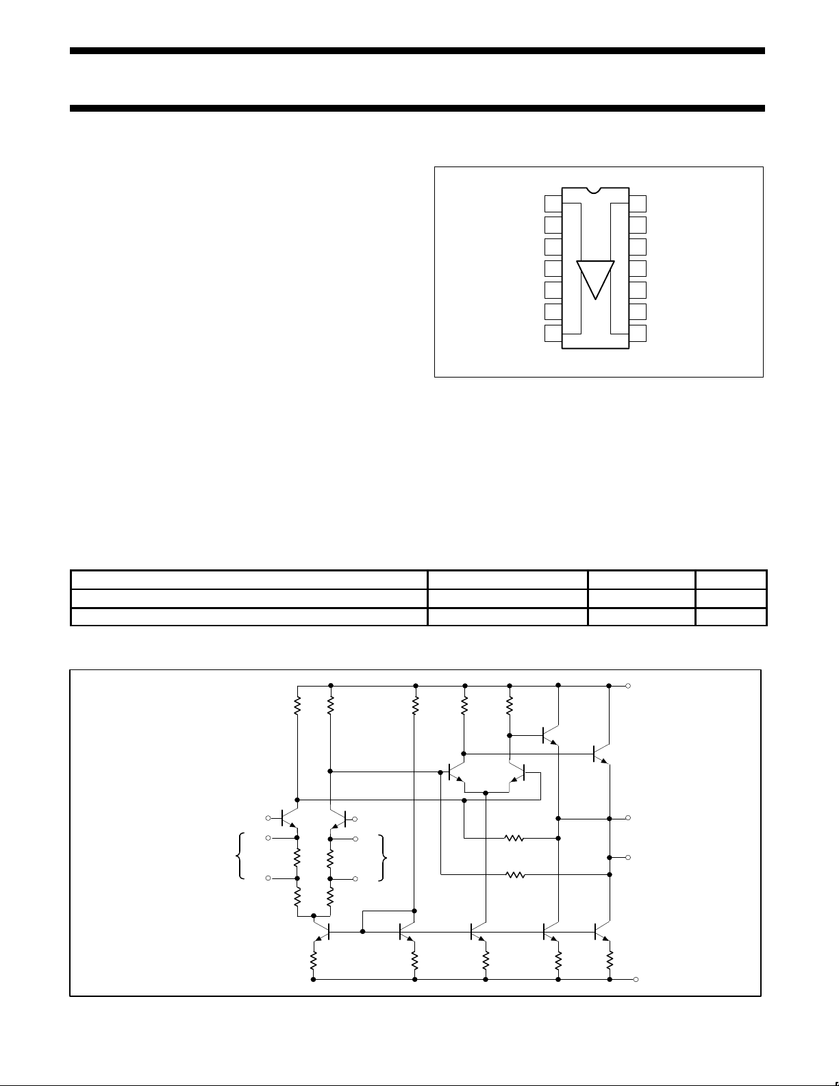
PIN CONFIGURA TION
N Package
1
2
NC
3
4
5
V–
6
NC
78
TOP VIEW
G
GAIN SELECT
2B
GAIN SELECT
G
1B
INPUT 2
OUTPUT 2
Figure 1. Pin Configuration
APPLICATIONS
•Video amplifier
•Pulse amplifier in communications
•Magnetic memories
•Video recorder systems
14
13
12
11
10
9
INPUT 1
NC
G
GAIN SELECT
2A
GAIN SELECT
G
1A
V+
NC
OUTPUT 1
SL00089
ORDERING INFORMATION
DESCRIPTION TEMPERATURE ORDER CODE DWG #
14-Pin Plastic Dual In–Line Package (DIP) -55°C to +125°C µA733N SOT27-1
14-Pin Plastic Dual In–Line Package (DIP) 0 to +70°C µA733CN SOT27-1
CIRCUIT SCHEMATIC
+V
R2 R8 R10 R9
R1
GAIN
SELECT
INPUT 1
G
G
1A
2A
2.4kΩ
Q1
R3 R5
50Ω
R4
590Ω
Q7
Q2
R7
300Ω
2.4kΩ
50Ω
R6
590Ω
INPUT 2
G
1B
G
2B
10kΩ
Q8 Q10
1.4kΩ
Figure 2. Circuit Schematic
Q3
1.1kΩ
Q9
300Ω
Q4
R11
7kΩ
R12
7kΩ
1.1kΩ
Q5
R12
400Ω
Q6
Q11
R14
400Ω
OUTPUT 1
OUTPUT 2
-V
SP00090
1992 Apr 15 853-1064 06456
2
Philips Semiconductors Product specification
SYMBOL
PARAMETER
TEST CONDITIONS
UNIT
µA733/733CDifferential video amplifier
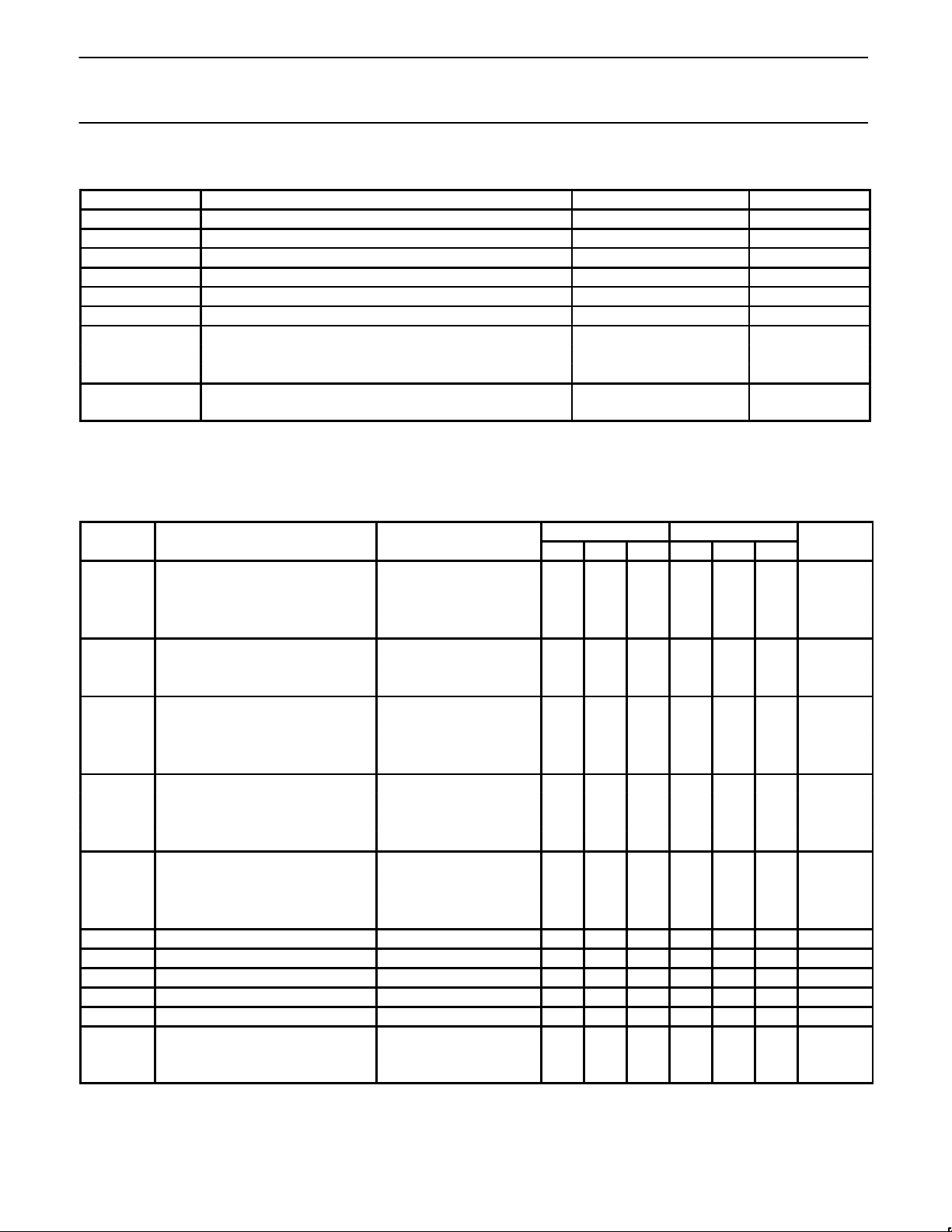
ABSOLUTE MAXIMUM RATINGS
SYMBOL PARAMETER RATING UNIT
V
DIFF
V
CM
V
CC
I
OUT
T
J
T
STG
T
A
P
D MAX
NOTE:
1. The following derating factors should be applied above 25°C:
N package at 11.4mW/°C
DC ELECTRICAL CHARACTERISTICS
TA=+25°C, VS=±6V, VCM=0, unless otherwise specified. Recommended operating supply voltages VS=±6.0V.
BW Gain 2
t
R
t
PD
R
IN
I
OS
I
BIAS
V
NOISE
V
IN
CMRR
Differential input voltage ±5 V
Common-mode input voltage ±6 V
Supply voltage ±8 V
Output current 10 mA
Junction temperature +150 °C
Storage temperature range -65 to +150 °C
Operating ambient temperature range
µA733C 0 to +70 °C
µA733 -55 to +125 °C
Maximum power dissipation, 1420 mW
25°C ambient temperature (still-air)
1
µA733C µA733
Min Typ Max Min Typ Max
Differential voltage gain RI = 2kΩ, V
2
Gain 1
2
Gain 2
3
Gain 3
1
Gain 1
2
3
Gain 3
V
V
OUT
OUT
1
Gain 1
2
Gain 2
3
Gain 3
1
Gain 1
2
Gain 2
3
Gain 3
2
Gain 1
2
Gain 2
3
Gain 3
Input capacitance
2
= 3V
OUT
P-P
250 400 600 300 400 500 V/V
80 100 120 90 100 110 V/V
8 10 12 9 10 11 V/V
40 40
90 90 MHz
120 120
= 1V
P-P
10.5 10.5 ns
4.5 12 4.5 10 ns
2.5 2.5 ns
= 1V
P-P
7.5 7.5 ns
6.0 10 6.0 10 ns
3.6 3.6 ns
4.0 4.0 kΩ
10 30 20 30 kΩ
250 250 kΩ
Gain 2 2.0 2.0 pF
Input offset current 0.4 5.0 0.4 3.0 µA
Input bias current 9.0 30 9.0 20 µA
Input noise voltage BW=1kHz to 10MHz 12 12 µV
Input voltage range ±1.0 ±1.0 V
Gain 2 VCM=±1V, f≤100kHz 60 86 60 86 dB
Gain 2 VCM=±1V, f=5MHz 60 60 dB
RMS
1992 Apr 15
3
 Loading...