

Philips tsa5518m DATASHEETS

INTEGRATED CIRCUITS
DATA SH EET
TSA5518M
1.3 GHz bidirectional I
controlled synthesizer
Product specification
File under Integrated Circuits, IC02
2
C-bus
1997 Mar 07
Philips Semiconductors Product specification
1.3 GHz bidirectional I2C-bus controlled
synthesizer
FEATURES
• Complete 1.3 GHz single chip system
• Low power 5 V, 40 mA
• I2C-bus programming
• One pin crystal oscillator
• In-lock flag
• Varicap drive disable
• Low radiation
• Address selection for picture in picture (PIP), DBS tuner,
and so on
• 5-level A/D converter
• 7 bus-controlled ports (4 open-collector outputs and
3 emitter follower outputs), 1 bidirectional port
• Power-down flag
• Mixer/oscillator bandswitch output
• Available in SSOP20 package.
APPLICATIONS
• TV tuners and front-ends
• VCR tuners.
TSA5518M
GENERAL DESCRIPTION
The device is a single chip PLL frequency synthesizer
designed for TV tuning systems. Control data is entered
via the I
the device, select the oscillator frequency, program the
7 output ports and set the charge-pump current.
The output port P6 is combined with an A/D converter
input. Digital information concerning this port can be read
out of the SDA line (one status byte) during a READ
operation. A flag is set when the loop is ‘in-lock’ and is read
during a READ operation. The device has one fixed
2
I
voltage on AS input. The phase comparator operates at
7.8125 kHz when a 4 MHz crystal in used. The device
provides a bandswitch output to select the bands of the
mixer/oscillator ICs TDA5330, TDA5630A except
TDA5630/C1 and TDA5730 with the appropriate voltage
level.
2
C-bus; five serial bytes are required to address
C-bus address, programmed by applying a specific
QUICK REFERENCE DATA
SYMBOL PARAMETER CONDITIONS MIN. TYP. MAX. UNIT
V
I
CC
f
i
V
CC
i(rms)
supply voltage 4.5 5 5.5 V
supply current − 40 − mA
frequency 80 − 1300 MHz
input voltage level (RMS value) 80 to 150 MHz 12 − 300 mV
150 MHz to 1.0 GHz 9 − 300 mV
1 GHz to 1.3 GHz 40 − 300 mV
f
I
xtal
o
crystal oscillator frequency 3.2 4 4.48 MHz
output current emitter follower on P4, P5 and P7 −−5mA
open-collector P0, P1 and P2 −−20 mA
open-collector P6 −−10 mA
T
R
amb
th j-a
operating ambient temperature −10 − +80 °C
thermal resistance from
−−120 K/W
junction to ambient
ORDERING INFORMATION
TYPE
NUMBER
NAME DESCRIPTION VERSION
PACKAGE
TSA5518M SSOP20 plastic shrink small outline package; 20 leads; body width 4.4 mm SOT266-1
1997 Mar 07 2
Philips Semiconductors Product specification
1.3 GHz bidirectional I2C-bus controlled
synthesizer
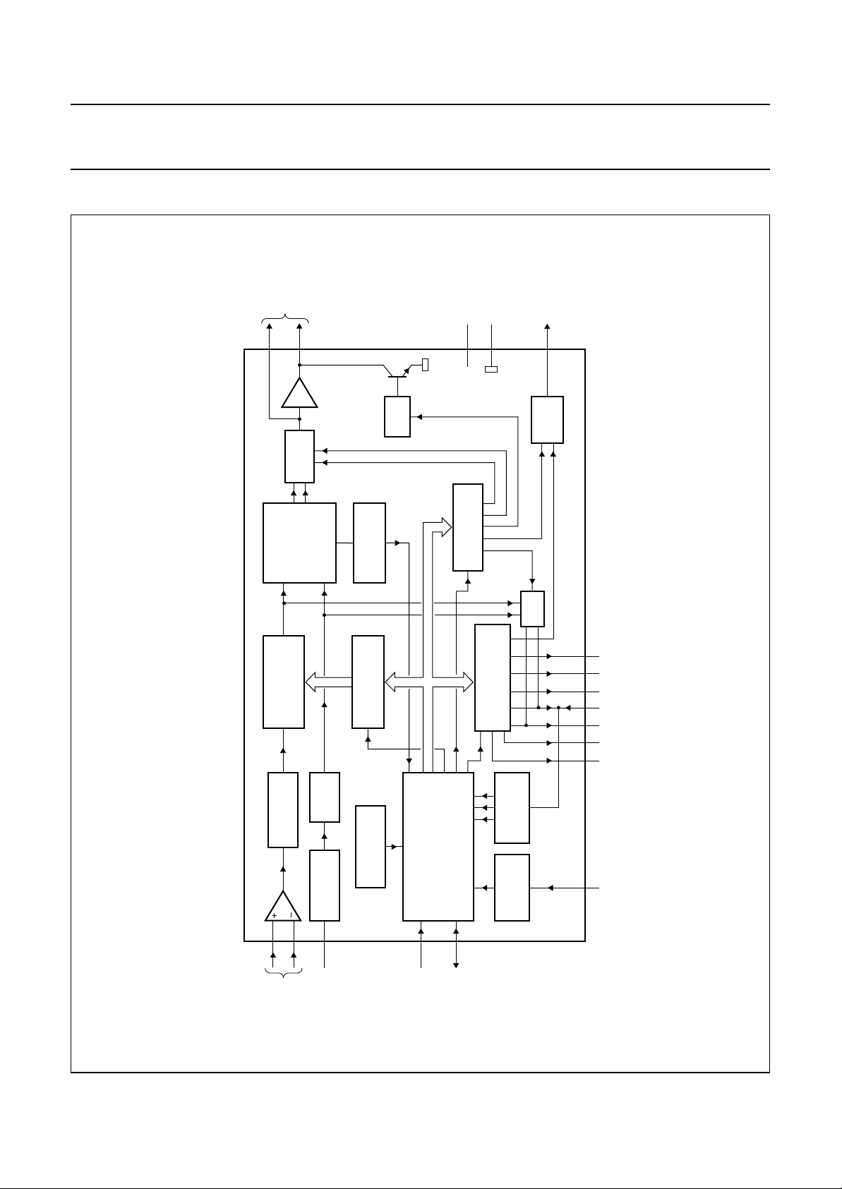
BLOCK DIAGRAM
output
PD
UD
1
20
PUMP
CHARGE
TO OP
LOGIC
OS
VCCGND
9
17
BS
5
BAND
SWITCH
TSA5518M
MGK115
PHASE
DIGITAL
COMPARATOR
DIV
f
15-BIT
DIVIDER
PROGRAMABLE
DIVIDE-BY-8
PRESCALER
8
7
ref
f
7.8125 kHz
N = 512
DIVIDER
4 MHz
OSCILLATOR
19
IN-LOCK
DETECTOR
15-BIT LATCH
DIVIDER RATIO
DETECTOR
POWER-DOWN
16
LATCH &
CONTROL DATA
C-BUS
2
I
TRANSCEIVER
15
8-BIT LATCH
PORT INFORMATION
T1
GATE
8-BIT A/D
CONVERTER
ADDRESS
SELECTION
handbook, full pagewidth
Fig.1 Block diagram.
1112 10 14 13 4 3 2
P0AS P1 P2 P6 P4 P5 P7
RF1
RF2
XTAL
input
1997 Mar 07 3
SCL
SDA

Philips Semiconductors Product specification
1.3 GHz bidirectional I2C-bus controlled
synthesizer
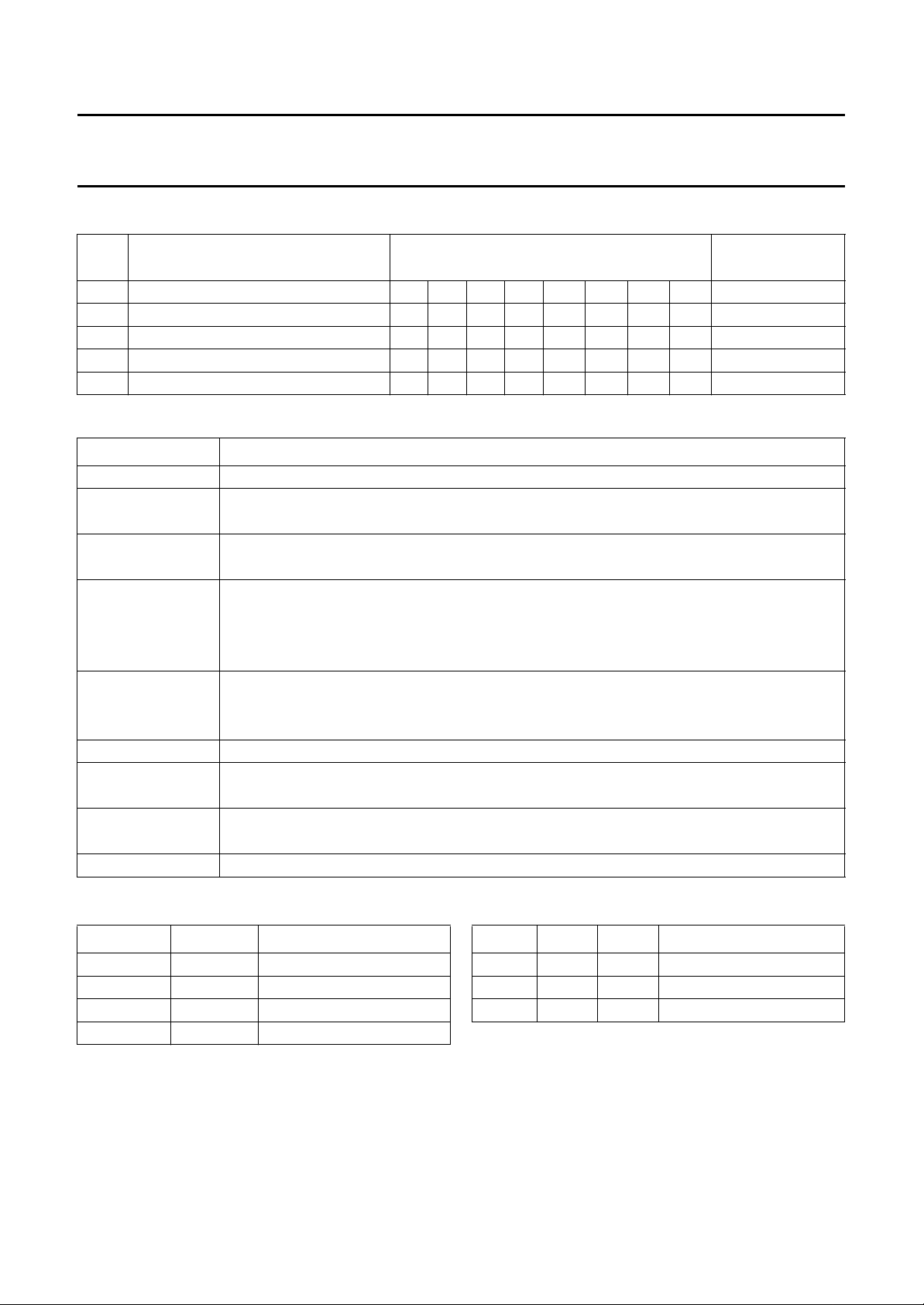
PINNING
SYMBOL PIN DESCRIPTION
UD 1 drive output (UD)
P7 2 P7 output port
P5 3 P5 output port
P4 4 P4 output port
BS 5 bandswitch output for M/O drive
n.c 6 not connected
RF2 7 UHF/VHF signal input 2
RF1 8 UHF/VHF signal input 1
GND 9 ground
P1 10 P1 output port (general purpose)
P0 11 P0 output port (general purpose)
AS 12 input for Address Selection
P6 13 P6 port (output/input for general
purpose ADC)
P2 14 P2 output port (f
is active)
2
SDA 15 I
SCL 16 I
V
CC
17 voltage supply
C-bus serial data input/output
2
C-bus serial clock
n.c 18 not connected
XTAL 19 crystal oscillator input
PD 20 charge-pump output (PD)
if the test mode
DIV
handbook, halfpage
TSA5518M
1
UD PD
2
P7 XTAL
3
P5 n.c.
4
P4
BS
5
P1
TSA5518M
6
7
8
9
10
n.c. SDA
RF2
RF1
GND
Fig.2 Pin configuration.
20
19
18
17
16
15
14
13
12
11
MBH947
V
CC
SCL
P2
P6
AS
P0
FUNCTIONAL DESCRIPTION
The device is controlled via the two wire I2C-bus.
For programming, there is one module address (7 bits)
and the R/W bit for selecting READ or WRITE mode.
Write mode
The write data format is summarized in Table 1. After the
address transmission (first byte), data bytes can be sent to
the device. Four data bytes are needed to fully program
the device. The bus transceiver has an auto increment
facility which permits the programming of the device within
one single transmission (address byte + 4 data bytes).
The device can also be partially programmed on the
condition that the first data byte following the address is
byte 2 or 4. The meaning of the bits in the data bytes is
given in Table 3. The first bit of the first data byte
transmitted indicates whether frequency data (first bit = 0)
1997 Mar 07 4
or charge pump and port information (first bit = 1) will
follow. Until an I
2
C-bus STOP condition is sent by the
controller, additional data bytes can be entered without the
need to re-address the device. This allows a smooth
frequency sweep for fine tuning or AFC purpose. At
power-on the ports are set to the high-impedance state
(open-collector outputs) or at the HIGH level (emitter
follower outputs). The bandswitch output BS provides a
voltage output suitable for the band selection input of
mixer/oscillator ICs TDA5330, TDA5630A and TDA5730.
It is controlled by B1 and B0 bits or P7, P5 and P4 bits
depending on the BSC bit (see Tables 1 to 4). The
7.8125 kHz reference frequency is obtained by dividing
the output of the 4 MHz crystal oscillator by 512. Because
the input of UHF/VHF signal is first divided-by-8 the step
size is 62.5 kHz. A 3.2 MHz crystal can offer step size of
50 kHz.
Philips Semiconductors Product specification
1.3 GHz bidirectional I2C-bus controlled
TSA5518M
synthesizer
Table 1 Write data format
BYTE DESCRIPTION
1 address 11000 MA1MA00 LOW from device
2 programmable divider 0 N14 N13 N12 N11 N10 N9 N8 LOW from device
3 programmable divider N7 N6 N5 N4 N3 N2 N1 N0 LOW from device
4 charge-pump, bandswitch and test bits 1 CP T1 T0 BSC B1 B0 OS LOW from device
5 output ports control bits P7 P6 P5 P4 X P2 P1 P0 LOW from device
Table 2 Explanation of Table 1
BIT DESCRIPTION
MA1, MA0 programmable address bits (see Table 7)
N14, .. , N0 programmable divider bits
14
N = N14 × 2
CP charge pump current
CP=0to50µA; CP=1to220µA
T1, T0, OS T1 = 0, T0 = 0, OS = 0: normal operation
T1 = 1: P2 = f
T0 = 1: 3-state charge pump
OS = 1: operational amplifier output is switched off (varicap drive disable)
BSC bandswitch control bit
BSC = 0: bandswitch output is controlled by B1 and B0 bits according to Table 3
BSC = 1: bandswitch output is controlled by P7, P5 and P4 bits according to Table 4
B1, B0 bandswitch control bits
P6, P2, P1 and P0 P6, P2 .. P0 = 1: open-collector outputs are active
P6, P2 .. P0 = 0: outputs are in high impedance state
P4, P5 and P7 P4, P5 and P7 = 1: outputs are at low level
P4, P5 and P7 = 0: emitter follower outputs are active
X don’t care
+ N13 × 213+...+ N1 × 21+N0
, P6 = f
DIV
MS
ref
B
LSB ACKNOWLEDGE
Table 3 BS output control (BSC = 0)
B1 B0 VOLTAGE ON PIN BS
0 0 0.25 V
01 2V
10 4V
11 V
1997 Mar 07 5
CC
Table 4 BS output control (BSC = 1)
P7 P5 P4 VOLTAGE ON PIN BS
1 1 0 0.25 V
101 2V
011 4V
Philips Semiconductors Product specification
1.3 GHz bidirectional I2C-bus controlled
TSA5518M
synthesizer
Read mode
The read data format is summarised in Table 5. Data can
be read out of the device by setting the R/W bit to logic 1.
After the slave address has been recognized, the device
generates an acknowledge pulse and the status word is
transferred on the SDA line (MSB first). Data is valid on the
SDA line during a HIGH of the SCL clock signal. A second
data byte can be read out of the device if the processor
generates an acknowledge on the SDA line. End of
transmission will occur if no acknowledge from the
processor occurs.The device will then release the data line
to allow the processor to generate a STOP condition.
When the port P6 is used as input, it must be programmed
Table 5 Read data format
BYTE DESCRIPTION MSB LSB ACKNOWLEDGE
1 address 11000MA1
2, .. status byte(s) POR
(2)
FL
(3)
000A2
in its high-impedance state. The POR flag (Power-on
reset) is set to logic 1 when V
goes below 3 V and at
CC
power-on. It is reset when an end of data is detected by the
device (end of a READ sequence). Control of the loop is
made possible with the in-lock flag FL which indicates
(FL = 1) when the loop is phase-locked. A built-in % level
A/D converter is available on I/O port P6. This converter
can be used to feed AFC information to the controller from
the IF section of the television as illustrated in the typical
application circuit in Fig.2. The relationship between bit
A2, A1 and A0 and the input voltage on port P6 is given in
Table 6.
(1)
(4)
MA0
A1
(4)
(1)
1 LOW from device
(4)
A0
note 5
Notes
1. See Table 7.
2. POR: Power-on reset flag. (POR = 1 on power-on).
3. FL: in lock flag (FL = 1 when the loop is phase-locked).
4. A2, A1, A0: digital outputs of the 5 level A/D converter (see Table 6). Accuracy is
1
⁄2LSB. MSB is transmitted first.
5. Upon an acknowledge pulse from the controller, the device transfers the status byte again. If no acknowledge pulse
from the controller is received, data read is terminated.
Table 6 A/D converter levels
Accuracy on the switching levels is ±0.02V
CC
.
VOLTAGE APPLIED ON PIN P6 A2 A1 A0
0.6V
0.45V
0.3V
0.15V
to 5.5 V 1 0 0
CC
to 0.6V
CC
to 0.45V
CC
to 0.3V
CC
0 to 0.15V
CC
CC
CC
CC
011
010
001
000
Address selection
The module address contains programmable address bits
(MA1 and MA0) which offer the possibility of having
several synthesizers (up to 3) in one system by applying a
specific voltage on AS input. The relationship between
MA1 and MA0 and the input voltage on AS input is given
in Table 7.
Frequency lock flag (FL) definition
When the FL flag is logic 1, the maximum frequency
Table 7 Address selection
VOLTAGE APPLIED ON PIN AS MA1 MA0
0 to 0.1V
CC
00
always valid 0 1
0.4 to 0.6V
CC
to V
0.9V
CC
CC
10
11
deviation dF from stable frequency can be expressed as:
K
VCO
± I
df
K
= oscillator slope (Hz/V)
VCO
I
= charge pump current (A)
CP
K
=4×10
O
------------K
O
×
6
CP
C1 C2+
×=
--------------------C1 C2×
with:
C1, C2 = loop filter capacitors.
1997 Mar 07 6
 Loading...