

Philips TSA5515T-C1 Datasheet

DATA SH EET
Product specification
File under Integrated Circuits, IC02
November 1991
INTEGRATED CIRCUITS
TSA5515T
1.3 GHz bi-directional I
2
C-bus
controlled synthesizer
November 1991 2
Philips Semiconductors Product specification
1.3 GHz bi-directional I2C-bus controlled synthesizer
TSA5515T
GENERAL DESCRIPTION
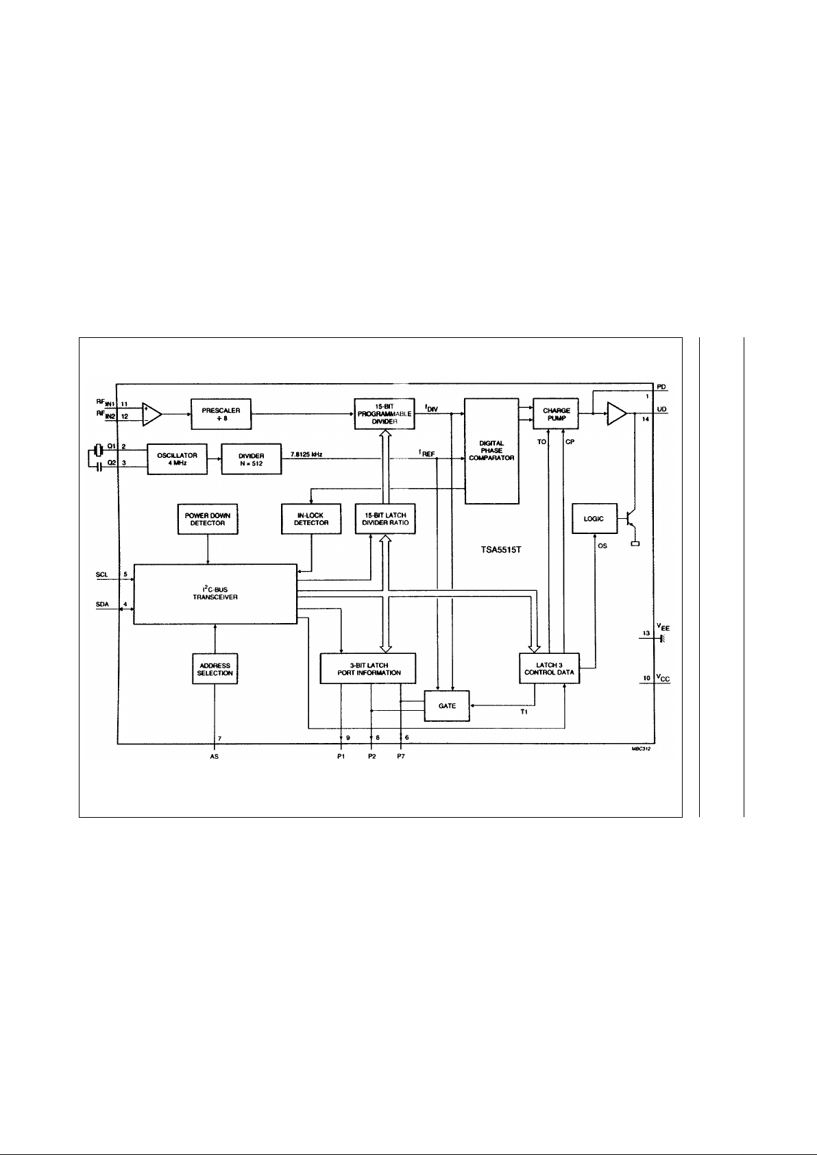
The TSA5515T is a single chip PLL frequency synthesizer
designed for TV tuning systems. Control data is entered
via the I2C-bus; five serial bytes are required to address
the device, select the oscillator frequency, programme the
three output ports and set the charge-pump current. A flag
is set when the loop is “in-lock”. Another flag is set when a
power dip occurs on the supply line. These flags are read
out of the TSA5515T on SDA line (one status byte) during
a READ operation. The device has 4 programmable
addresses, programmed by applying a specific voltage on
the AS pin. The phase comparator operates at
7.8125 kHz when a 4 MHz crystal is used.
FEATURES
• Complete 1.3 GHz single-chip system
• Low power 5 V, 35 mA
• I
2
C-bus programming
QUICK REFERENCE DATA
ORDERING INFORMATION
Note
1. SOT108-1; 1996 December 3.
SYMBOL PARAMETER MIN. TYP. MAX. UNIT
V
CC
supply voltage − 5 − V
I
CC
supply current − 35 − mA
∆f frequency range 64 − 1300 MHz
V
I (RMS)
input voltage level (RMS value)
80 MHz to 150 MHz 12 − 300 mV
150 MHz to 1 GHz 9 − 300 mV
1 GHz to 1.3 GHz 40 − 300 mV
f
XTAL
crystal oscillator 3.2 4 4.48 MHz
I
O
open-collector output current
P7 −−5mA
P1, P2 −−20 mA
T
amb
operating ambient temperature range −10 − 80 °C
T
stg
storage temperature range −40 − 125 °C
R
th j-a
thermal resistance − 110 − K/W
EXTENDED TYPE NUMBER
PACKAGE
PINS PIN POSITION MATERIAL CODE
TSA5515T 14 SO plastic SOT108A
(1)
• In-lock flag
• Varicap drive disable
• Low radiation
• Address selection for Picture-In-Picture (PIP), DBS
tuner, etc.
• 3 bus-controlled output ports
• Power-down flag
• Available in SOT108A package
APPLICATIONS
• TV tuners
• VCR tuners
November 1991 3
Philips Semiconductors Product specification
1.3 GHz bi-directional I
2
C-bus controlled synthesizer
TSA5515T
Fig.1 Block diagram
November 1991 4
Philips Semiconductors Product specification
1.3 GHz bi-directional I2C-bus controlled synthesizer
TSA5515T
LIMITING VALUES
In accordance with Absolute Maximum System (IEC 134).
THERMAL RESISTANCE
HANDLING
Every pin withstands the ESD test in accordance with MIL-STD-883C, category A (> 1500 V).
SYMBOL PARAMETER MIN. MAX. UNIT
V
CC
supply voltage −0.3 6 V
V
P1
charge-pump output voltage −0.3 V
CC
V
V
P2
crystal (Q1) input voltage −0.3 V
CC
V
V
P4
serial data input/output −0.3 6 V
V
P5
serial clock input −0.3 6 V
V
P7
address selection −0.3 6 V
V
P6
output ports P7, P2, P1 −0.3 16 V
V
P11
prescaler inputs −0.3 2.5 V
V
P14
drive output −0.3 V
CC
V
I
6L
output port P7 (open collector) −110mA
I
8L
output port P2, P1 (open collector) −125mA
I
4L
SDA output (open collector) −15 mA
T
stg
storage temperature range −40 125 °C
T
j
junction temperature − 125 °C
SYMBOL PARAMETER THERMAL RESISTANCE
R
th j-a
from junction to ambient in free air 110 K/W
November 1991 5
Philips Semiconductors Product specification
1.3 GHz bi-directional I2C-bus controlled synthesizer
TSA5515T
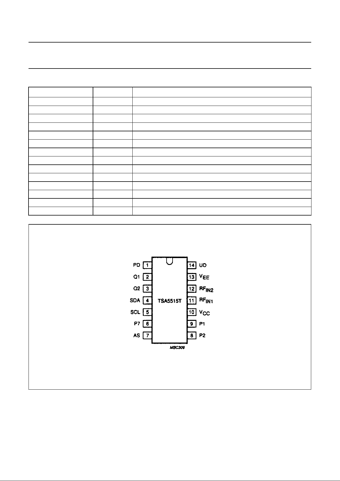
PINNING
SYMBOL PIN DESCRIPTION
PD 1 charge-pump output
Q1 2 crystal oscillator input 1
Q2 3 crystal oscillator input 2
SDA 4 serial data input/output
SCL 5 serial clock input
P7 6 port output
AS 7 input for address selection
P2 8 port output
P1 9 port output
V
CC
10 voltage supply
RF
IN1
11 UHF/VHF signal input 1
RF
IN2
12 UHF/VHF signal input 2 (decoupled)
GND 13 ground
UD 14 drive output
Fig.2 Pinning diagram.
 Loading...