

Philips TSA5512AT, TSA5512AM, TSA5512, TSA5512T Datasheet

DATA SH EET
Product specification
File under Integrated Circuits, IC02
October 1992
INTEGRATED CIRCUITS
TSA5512
1.3 GHz Bidirectional I
2
C-bus
controlled synthesizer
October 1992 2
Philips Semiconductors Product specification
1.3 GHz Bidirectional I2C-bus controlled synthesizer
TSA5512
FEATURES
• Complete 1.3 GHz single chip system
• Low power 5 V, 35 mA
• I2C-bus programming
• In-lock flag
• Varicap drive disable
• Low radiation
• Address selection for Picture-In-Picture (PIP), DBS
tuner (3 addresses)
• Analog-to-digital converter
• 8 bus controlled ports (6 for TSA5512T), 8 open
collector outputs (4 bidirectional)
• Power-down flag
APPLICATIONS
• TV tuners
• VCR Tuners
DESCRIPTION
The TSA5512 is a single chip PLL frequency synthesizer
designed for TV tuning systems. Control data is entered
via the I2C-bus; five serial bytes are required to address
the device, select the oscillator frequency, programme the
eight output ports and set the charge-pump current. Four
of these ports can also be used as input ports (three
general purpose I/O ports, one ADC). Digital information
concerning those ports can be read out of the TSA5512 on
the SDA line (one status byte) during a READ operation. A
flag is set when the loop is “in-lock” and is read during a
READ operation. The device has one fixed I2C-bus
address and 3 programmable addresses, programmed by
applying a specific voltage on Port 3. The phase
comparator operates at 7.8125 kHz when a 4 MHz crystal
is used.
ORDERING INFORMATION
Note
1. SOT102-1; 1996 December 5.
2. SOT109-1; 1996 December 5.
3. SOT163-1; 1996 December 5.
4. SOT266-1; 1996 December 5.
EXTENDED TYPE
NUMBER
PACKAGE
PINS PIN POSITION MATERIAL CODE
TSA5512 18 DIL plastic SOT102
(1)
TSA5512T 16 SO plastic SOT109A
(2)
TSA5512AT 20 SO plastic SOT163A
(3)
TSA5512M 20 SSOP plastic SOT266
(4)
October 1992 3
Philips Semiconductors Product specification
1.3 GHz Bidirectional I2C-bus controlled synthesizer
TSA5512
QUICK REFERENCE DATA
SYMBOL PARAMETER MIN. TYP. MAX. UNIT
V
CC
supply voltage − 5 − V
I
CC
supply current − 35 − mA
∆fr frequency range 64 − 1300 MHz
V
I
input voltage level
80 MHz to 150 MHz 12 − 300 mV
150 MHz to 1 GHz 9 − 300 mV
1 GHz to 1.3 GHz 40 − 300 mV
f
XTAL
crystal oscillator frequency 3.2 4.0 4.48 MHz
I
O
open-collector output current 5 −−mA
T
amb
operating ambient temperature range −10 − +80 °C
T
stg
IC storage temperature range −40 − +150 °C
October 1992 4
Philips Semiconductors Product specification
1.3 GHz Bidirectional I2C-bus controlled
synthesizer
TSA5512
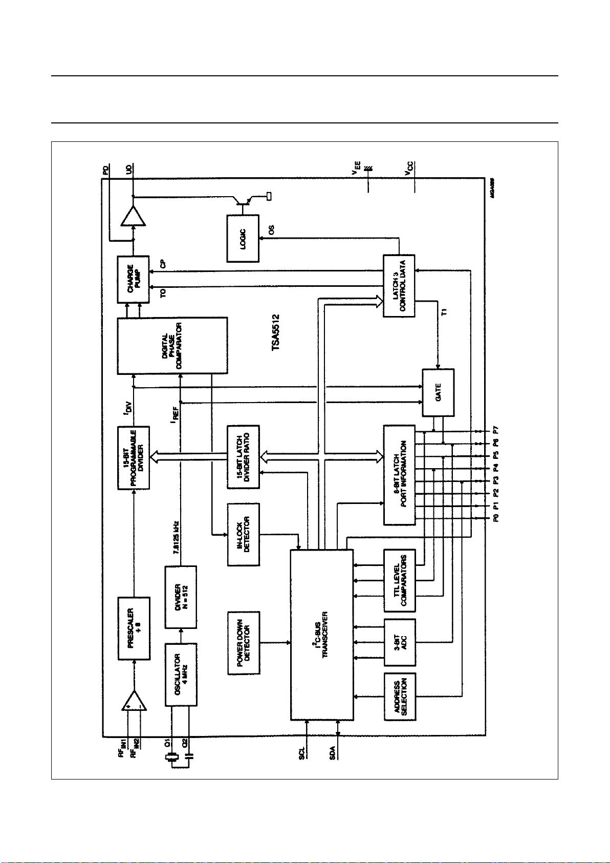
Fig.1 Block diagram.
October 1992 5
Philips Semiconductors Product specification
1.3 GHz Bidirectional I2C-bus controlled synthesizer
TSA5512
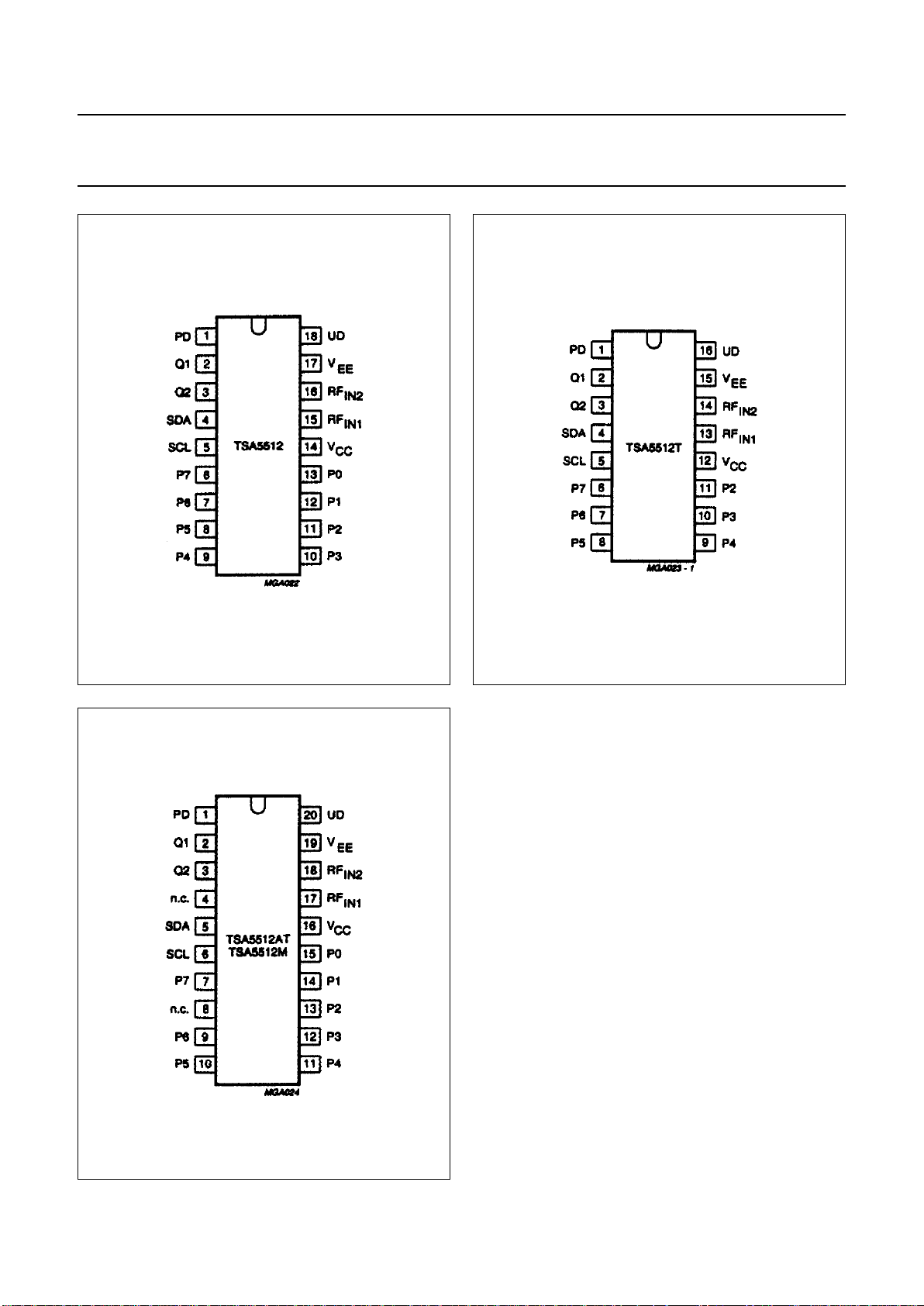
Fig.2 Pin configuration for SOT102. Fig.3 Pin configuration for SOT109.
Fig.4 Pin configuration for SOT163/SOT266.

October 1992 6
Philips Semiconductors Product specification
1.3 GHz Bidirectional I2C-bus controlled synthesizer
TSA5512
PINNING
FUNCTIONAL DESCRIPTION
The TSA5512 is controlled via the two-wire I
2
C-bus. For programming, there is one module address (7 bits) and the R/W
bit for selecting READ or WRITE mode.
WRITE mode: R/W = 0 (see Table 1)
After the address transmission (first byte), data bytes can be sent to the device. Four data bytes are required to fully
program the TSA5512. The bus transceiver has an auto-increment facility which permits the programming of the
TSA5512 within one single transmission (address + 4 data bytes).
The TSA5512 can also be partially programmed on the condition that the first data byte following the address is byte 2
or byte 4. The meaning of the bits in the data bytes is given in Table 1. The first bit of the first data byte transmitted
indicates whether frequency data (first bit = 0) or charge pump and port information (first bit = 1) will follow. Until an
I2C-bus STOP condition is sent by the controller, additional data bytes can be entered without the need to re-address the
device. This allows a smooth frequency sweep for fine tuning or AFC purpose. At power-on the ports are set to the high
impedance state.
The 7.8125 kHz reference frequency is obtained by dividing the output of the 4 MHz crystal oscillator by 512.
Because the input of UHF/VHF signal is first divided by 8 the step size is 62.5 kHz. A 3.2 MHz crystal can offer step sizes
of 50 kHz.
SYMBOL
PIN
DESCRIPTION
SOT102 SOT109
SOT163
SOT266
PD 1 1 1 charge-pump output
Q1 2 2 2 crystal oscillator input 1
Q2 3 3 3 crystal oscillator reference voltage
n.c. −−4 not connected
SDA 4 4 5 serial data input/output
SCL 5 5 6 serial clock input
P7 6 6 7 port output/input (general purpose)
n.c. −−8 not connected
P6 7 7 9 port output/input for general purpose ADC
P5 8 8 10 port output/input (general purpose)
P4 9 9 11 port output/input (general purpose)
P3 10 10 12 port output/input for address selection
P2 11 11 13 port output
P1 12 − 14 port output
P0 13 − 15 port output
V
CC
14 12 16 voltage supply
RF
IN1
15 13 17 UHF/VHF signal input 1
RF
IN2
16 14 18 UHF/VHF signal input 2 (decoupled)
V
EE
17 15 19 ground
UD 18 16 20 drive output
 Loading...