

Philips TSA5059 Datasheet
INTEGRATED CIRCUITS
DATA SH EET
TSA5059
2.7 GHz I
2
C-bus controlled
low phase noise frequency
synthesizer
Preliminary specification
File under Integrated Circuits, IC02
1999 Oct 05

Philips Semiconductors Preliminary specification
2.7 GHz I2C-bus controlled low phase
noise frequency synthesizer
FEATURES
• Complete 2.7 GHz single chip system
• Optimized for low phase noise
• Selectable divide-by-two prescaler
• Operation up to2.7 GHz with and without divide-by-two
prescaler
• Selectable reference divider ratio
• Compatible with UK-DTT (Digital Terrestrial Television)
offset requirements
• Selectable crystal/comparison frequency output
• Four selectable charge pump currents
• Four selectable I2C-bus addresses
• Standard and fast mode I2C-bus
• I2C-bus compatible with 3.3 and 5 V microcontrollers
• 5-level Analog-to-Digital Converter (ADC)
• Low power consumption
• 33 V tuning voltage drive
• Three I/O ports and one output port.
APPLICATIONS
• SAT, TV, VCR and cable tuning systems
• Digital set-top boxes.
GENERAL DESCRIPTION
The TSA5059 is a single chip PLL frequency synthesizer
designed for satellite and terrestrial tuning systems up to
2.7 GHz.
TheRFpreamplifierdrivesthe 17-bit main divider enabling
astep size equal tothe comparison frequency, for aninput
frequency up to 2.7 GHz. A fixed divide-by-two additional
prescaler can be inserted between the preamplifier and
the main divider to give a software compatibility with
TSA5059
existing ICs. In this case, the step size is twice the
comparison frequency.
The comparison frequency is obtained from an on-chip
crystal oscillator that can also be driven from an external
source. Either the crystal frequency or the comparison
frequency can be switched to the XT/COMP output pin to
drive the reference input of another synthesizer or the
clock input of a digital demodulation IC.
Bothdividedandcomparisonfrequencyarecomparedinto
the fast phase detector which drives the charge pump.
The loop amplifier is also on-chip, including the
high-voltage transistor to drive directly the 33 V tuning
voltage, without the need of an external transistor.
ControldataisenteredviatheI2C-bus;fiveserialbytesare
required to address the device, select the main divider
ratio, the reference divider ratio, program the four output
ports,set the charge pump current, selectthe prescaler by
two, select the signal to switch to the XT/COMP output pin
and/or select a specific test mode. Three of the four output
ports can also be used as input ports and a 5-level ADC is
provided. Digital information concerning the input ports
and the ADC can be read out of the TSA5059 on the SDA
line (one status byte) during a READ operation. A flag is
set when the loop is ‘in-lock’ and is read during a READ
operation, as well as the Power-on reset flag. The device
has four programmable addresses, programmed by
applying a specific voltage at pin AS, enabling the use of
multiple synthesizers in the same system.
1999 Oct 05 2
Philips Semiconductors Preliminary specification
2.7 GHz I2C-bus controlled low phase
TSA5059
noise frequency synthesizer
QUICK REFERENCE DATA
VCC= 4.5 to 5.5 V; T
SYMBOL PARAMETER CONDITIONS MIN. TYP. MAX. UNIT
V
CC
I
CC
f
i(RF)
V
i(RF)(rms)
f
xtal
T
amb
T
stg
supply voltage 4.5 5.0 5.5 V
supply current T
RF input frequency 64 − 2700 MHz
RF input voltage (RMS value) f
crystal frequency 4 − 16 MHz
ambient temperature −20 − +85 °C
storage temperature −40 − +150 °C
Note
1. Asymmetrical drive on pin RFA or RFB; see Fig.3.
= −20 to +85 °C; unless otherwise specified.
amb
=25°C 303745mA
amb
from 64 to 150 MHz;
i(RF)
note 1
f
from 150 to 2200 MHz;
i(RF)
note 1
f
from 2.2 to 2.7 GHz;
i(RF)
note 1
12.6 − 300 mV
−25 − +2.5 dBm
7.1 − 300 mV
−30 − +2.5 dBm
22.4 − 300 mV
−20 − +2.5 dBm
ORDERING INFORMATION
TYPE
NUMBER
NAME DESCRIPTION VERSION
PACKAGE
TSA5059T SO16 plastic small outline package; 16 leads; body width 3.9 mm SOT109-1
TSA5059TS SSOP16 plastic shrink small outline package; 16 leads; body width 4.4 mm SOT369-1
1999 Oct 05 3
Philips Semiconductors Preliminary specification
2.7 GHz I2C-bus controlled low phase
noise frequency synthesizer
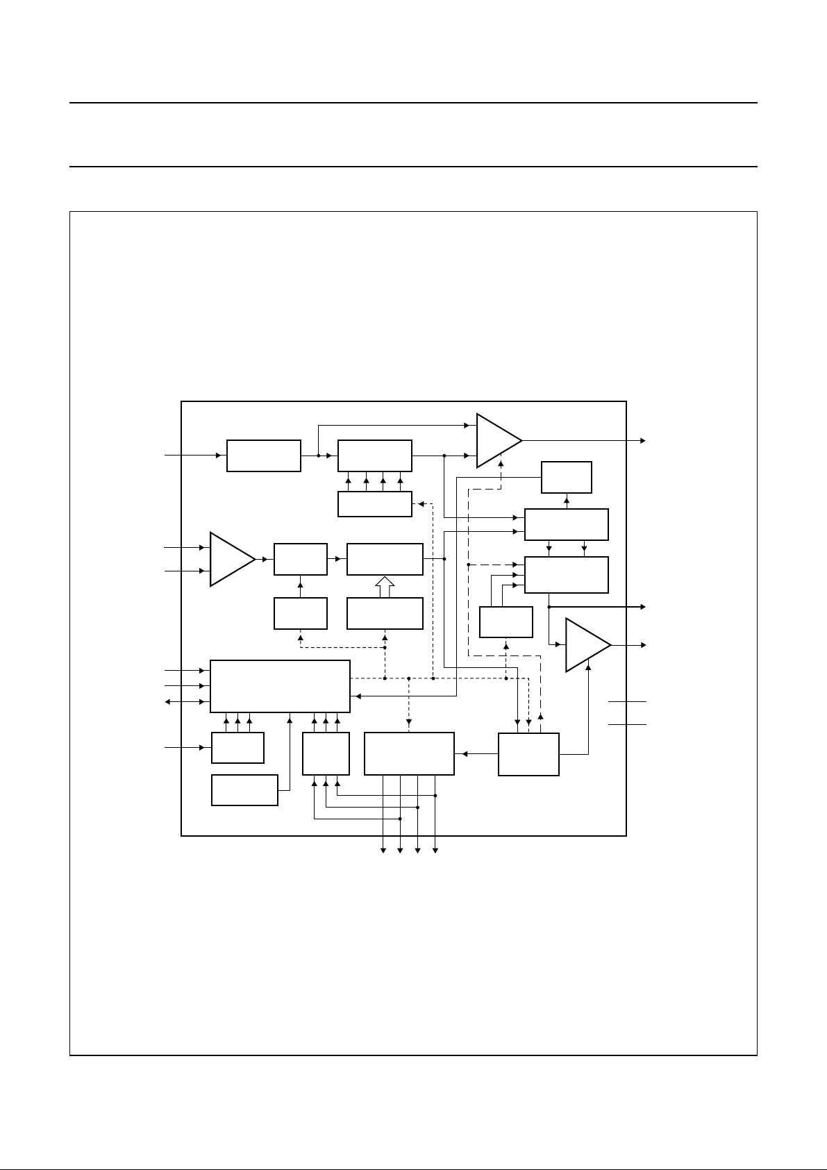
BLOCK DIAGRAM
handbook, full pagewidth
XTAL
RFA
RFB
2
13
14
OSCILLATOR
PRE
AMP
XTAL
DIVIDER
1/2
REFERENCE
DIVIDER
4-BIT LATCH
17-BIT
DIVIDER
LOCK
DETECT
DIGITAL PHASE
COMPARATOR
CHARGE PUMP
3
TSA5059
XT/COMP
AS
SCL
SDA
ADC
4
6
5
11
TRANSCEIVER
3-BIT
ADC
POWER-ON
RESET
1-BIT
LATCH
I2C-BUS
3-BIT
INPUT
PORTS
17-BIT LATCH
DIVIDE RATIO
4-BIT LATCH
AND
OUTPUT PORTS
P3 P2 P1 P0
1
2-BIT
LATCH
CONTROL
MODE
LOGIC
33 V
AMP
CP
16
VT
12
V
CC
15
GND
TSA5059
10987
FCE120
Fig.1 Block diagram.
1999 Oct 05 4
Philips Semiconductors Preliminary specification
2.7 GHz I2C-bus controlled low phase
noise frequency synthesizer
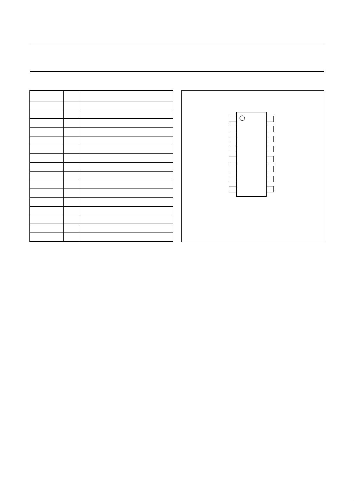
PINNING
SYMBOL PIN DESCRIPTION
CP 1 charge pump output
XTAL 2 crystal oscillator input
XT/COMP 3 f
AS 4 I
SDA 5 I
SCL 6 I
P3 7 general purpose output Port 3
P2 8 general purpose input/output Port 2
P1 9 general purpose input/output Port 1
P0 10 general purpose input/output Port 0
ADC 11 analog-to-digital converter input
V
CC
12 supply voltage
RFA 13 RF signal input A
RFB 14 RF signal input B
GND 15 ground supply
VT 16 tuning voltage output
or f
xtal
2
C-bus address selection input
2
C-bus serial data input/output
2
C-bus serial clock input
signal output
comp
handbook, halfpage
XT/COMP
CP
1
XTAL
2
3
AS
4
SDA
SCL
P3
P2
TSA5059
5
6
7
8
FCE121
Fig.2 Pin configuration.
16
VT
15
GND
14
RFB
13
RFA
V
12
CC
ADC
11
10
P0
P1
9
TSA5059
FUNCTIONAL DESCRIPTION
The TSA5059 contains all the necessary elements but a
referencesourceandaloopfilterto control a varicap tuned
local oscillator forming a phase locked loop frequency
synthesized source. The IC is designed in a high speed
process with a fast phase detector to allow a high
comparison frequency to reach a low phase noise level on
the oscillator.
The block diagram is shown in Fig.1. The RF signal is
applied at pins RFA and RFB. Thanks to the input
preamplifier a good sensitivity is provided. The output of
the preamplifier is fed to the 17-bit programmable divider
either through a divide-by-two prescaler or directly.
Becauseof the internal high speed process, theRF divider
is working for a frequency up to 2.7 GHz, without the need
for the divide-by-two prescaler to be used. This prescaler
is present on chip for compatibility reasons with existing
circuits.
The output of the 17-bit programmable divider f
DIV
is fed
into the phase comparator, where it is compared in both
phaseandfrequency with the comparison frequency f
comp
This frequency is derived from the signal present at
pin XTAL, f
, divided down in the reference divider. It is
xtal
possible either to connect a quartz crystal topin XTAL and
then using the on-chip crystal oscillator, or to feed this pin
with a reference signal from an external source.
The reference divider can have a dividing ratio selected
from 16 different values between 2 and 320, including the
ratio 24 to cope with the offset requirement of the UK-DTT
system, see Table 8.
The output of the phase comparator drives the
charge pump and the loop amplifier section. This amplifier
has an on-chip high voltage drive transistor which avoids
the use of an additional external component. Pin CP is the
output of the charge pump, and pin VT is the pin to drive
the tuning voltage to the varicap diode of the Voltage
Controlled Oscillator (VCO). The loop filter has to be
connected between pins CP and VT.
In addition, it is possible to drive another PLL synthesizer,
or the clock input of a digital demodulation IC, from the
pin XT/COMP. It is possible to select by software either
f
, the crystal oscillator frequency or f
xtal
, the frequency
comp
present after the reference divider at this pin. It is also
possible to switch off this output, in case it is not used.
For test and alignment purposes, it is possible to release
.
the tuning voltage output to be able to apply an external
voltage on it, to select one of the three charge pump test
modes, and to monitor half the f
at Port P0. See
DIV
Table 10 for all possible modes.
1999 Oct 05 5
Philips Semiconductors Preliminary specification
2.7 GHz I2C-bus controlled low phase
noise frequency synthesizer
Four open-collector output ports are provided on the IC for
general purpose; three of these can also be used as input
ports. A 3-bit ADC is also available.
The TSA5059 is controlled via the two-wire I2C-bus.
For programming, there is one 7-bit module address and
the R/W bit for selecting READ or WRITE mode. To be
able to have more than one synthesizer in an I2C-bus
system, one of four possible addresses is selected
depending on the voltage applied at pin AS (see Table 3).
The TSA5059 fulfils the fast mode I2C-bus, according to
the Philips I2C-bus specification. The I2C-bus interface is
designed in such a way that pins SCL and SDA can be
connected either to 5 or to 3.3 V pulled-up I2C-bus lines,
allowing the PLL synthesizer to be connected directly to
the bus lines of a 3.3 V microcontroller.
WRITE mode: R/W=0
After the address transmission (first byte), data bytes can
be sent to the device (see Table 1). Four data bytes are
neededtofullyprogramtheTSA5059. The bus transceiver
hasan auto-increment facility that permitsprogramming of
the TSA5059 within one single transmission
(address + 4 data bytes).
TSA5059
The TSA5059 can also be partly programmed on the
condition that the first data byte following the address is
byte 2 or byte 4. The meaning of the bits in the data bytes
is given in Table 1. The first bit of the first data byte
transmitted indicates whether byte 2 (first bit is logic 0) or
byte 4 (first bit is logic 1) will follow. Until an I2C-bus STOP
condition is sent by the controller, additional data bytes
can be entered without the need to re-address the device.
To allow a smooth frequency sweep for fine tuning, and
while the data of the dividing ratio of the main divider is in
data bytes 2, 3 and 4, it is necessary for changing the
frequency to send the data bytes 2 to 5 in a repeated
sending, or to finish an incomplete transmission by a
STOP condition. Repeated sending of data bytes 2 and 3
without ending the transmission does not change the
dividing ratio. To illustrate, the following data sequences
will change the dividing ratio:
• Bytes 2, 3, 4 and 5
• Bytes 4, 5, 2 and 3
• Bytes 2, 3, 4 and STOP
• Bytes 4, 5, 2 and STOP
• Bytes 2, 3 and STOP
• Bytes 2 and STOP
• Bytes 4 and STOP.
Table 1 Write data format
BYTE DESCRIPTION MSB
1 address 1 1 0 0 0 MA1 MA0 0 A
2 programmable divider 0 N14 N13 N12 N11 N10 N9 N8 A
3 programmable divider N7 N6 N5 N4 N3 N2 N1 N0 A
4 control data 1 N16 N15 PE R3 R2 R1 R0 A
5 control data C1 C0 XCE XCS P3 P2/T2 P1/T1 P0/T0 A
Note
1. MSB is transmitted first.
(1)
LSB CONTROL BIT
1999 Oct 05 6
Philips Semiconductors Preliminary specification
2.7 GHz I2C-bus controlled low phase
TSA5059
noise frequency synthesizer
Table 2 Explanation of Table 1
BIT DESCRIPTION
MA1 and MA0 programmable address bits; see Table 3
A acknowledge bit
N16 to N0 programmable main divider ratio control bits; N = N16 × 216+ N15 × 215+ ... + N1 × 21+N0
PE prescaler enable (prescaler by 2 is active when bit PE = 1)
R3 to R0 programmable reference divider ratio control bits; see Table 8
C1 and C0 charge pump current select bits; see Table 9
XCE XT/COMP enable; XT/COMP output active when bit XCE = 1; see Table 10
XCS XT/COMP select; signal select when bit XCE = 1, test mode enable when bit XCE = 0; see Table 10
T2, T1 and T0 test mode select when bit XCE = 0 and bit XCS = 1; see Table 10
P3, P2 and P1 Port P3, P2 and P1 output states
P0 Port P0 output state, except in test mode; see Table 10
Address selection (see Table 3)
The module address contains programmable address bits (MA1 and MA0), which offer the possibility of having
up to 4 synthesizers in one system. The relationship between MA1 and MA0 and the input voltage at pin AS is given in
Table 3.
Table 3 Address selection
MA1 MA0 VOLTAGE APPLIED TO PIN AS
0 0 0 to 0.1V
CC
0 1 open-circuit
1 0 0.4V
1 1 0.9V
to 0.6VCC; note 1
CC
to V
CC
CC
Note
1. This address is selected by connecting a 15 kΩ resistor between pin AS and pin V
CC
.
Status at Power-On Reset (POR)
At power-on or when the supply voltage drops below approximately 2.75 V, internal registers are set according to
Table 4.
Table 4 Status at Power-on reset; note 1
BYTE DESCRIPTION MSB LSB CONTROL BIT
1 address 11000MA1MA00 A
2 programmable divider 0 XXXXXXX A
3 programmable divider XXXXXXXX A
4 control data 1 XXXXXXX A
5 control data 0001X
(2)
(2)
1
(2)
X
(2)
X
A
Notes
1. X = don’t care.
2. At Power-on reset, all output ports are in high-impedance state.
1999 Oct 05 7
Philips Semiconductors Preliminary specification
2.7 GHz I2C-bus controlled low phase
TSA5059
noise frequency synthesizer
READ mode: R/W=1
Data can be read out of the TSA5059 by setting the
bit R/W to logic 1 (see Table 5). After the slave address
has been recognized, the TSA5059 generates an
acknowledge pulse and the first data byte (status word) is
transferredontheSDA line(MSBfirst). Data is valid on the
SDA line during a HIGH-level of the SCL clock signal.
A second data byte can be read out of the TSA5059 if the
controller generates an acknowledge on the SDA line.
End of transmission will occur if no acknowledge from the
controller occurs.The TSA5059 will then release the data
line to allow the controller to generate a STOP condition.
When ports P0 to P2 are used as inputs, they must be
programmed in their high-impedance state.
The POR flag is set to logic 1 when VCC drops below
approximately 2.75 V and at power-on.
Table 5 Read data format
BYTE DESCRIPTION MSB
(1)
1 address 1 1000MA1MA01 A
2 status byte POR FL I2 I1 I0 A2 A1 A0 −
It is reset to logic 0 when an end of data is detected by the
TSA5059 (end of a READ sequence).
Control of the loop is made possible with the in-lock flag
which indicates (bit FL = 1) whenthe loop is phase-locked.
The bits I2, I1 and I0 represent the status of the I/O ports
P2, P1 and P0 respectively. A logic 0 indicates a
LOW-level and a logic 1 indicates a HIGH-level.
A built-in 5-level ADC is available at pin ADC. This
converter can be used to feed AFC information to the
microcontroller through the I2C-bus. The relationship
between bits A2, A1, A0 and the input voltage at pin ADC
is given in Table 7.
LSB CONTROL BIT
Note
1. MSB is transmitted first.
Table 6 Explanation of Table 5
BIT DESCRIPTION
A acknowledge bit
MA1 and MA0 programmable address bits; see Table 3
POR Power-on reset flag (bit POR = 1 on power-on)
FL in-lock flag (bit FL = 1 when the loop is phase-locked)
I2, I1 and I0 digital information for I/O ports P2, P1 and P0 respectively
A2, A1 and A0 digital outputs of the 5-level ADC; see Table 7
Table 7 ADC levels
A2 A1 A0 VOLTAGE APPLIED TO PIN ADC
1 0 0 0.6VCCto V
0 1 1 0.45VCCto 0.6V
0 1 0 0.3VCCto 0.45V
0 0 1 0.15VCCto 0.3V
0 0 0 0 to 0.15V
CC
CC
CC
CC
CC
Note
1. Accuracy is ±0.03V
CC
.
(1)
1999 Oct 05 8
 Loading...