

Page 1

INTEGRATED CIRCUITS
DATA SH EET
TJA1050
High speed CAN transceiver
Product specification
Supersedes data of 2002 May 16
2003 Oct 22
Page 2
Philips Semiconductors Product specification
High speed CAN transceiver TJA1050
FEATURES
• Fully compatible with the
“ISO 11898”
standard
• High speed (up to 1 Mbaud)
• Very low ElectroMagnetic Emission (EME)
• Differential receiver with wide common-mode range for
high ElectroMagnetic Immunity (EMI)
• An unpowered node does not disturb the bus lines
• Transmit Data (TXD) dominant time-out function
• Silent mode in which the transmitter is disabled
• Bus pins protected against transients in an automotive
environment
• Input levels compatible with 3.3 V and 5 V devices
• Thermally protected
• Short-circuit proof to battery and to ground
• At least 110 nodes can be connected.
GENERAL DESCRIPTION
The TJA1050 isthe interface between the Controller Area
Network (CAN) protocol controller and the physical bus.
The device provides differential transmit capability to the
bus and differential receive capability to the CAN
controller.
The TJA1050 is the third Philips high-speed CAN
transceiver after the PCA82C250 and the PCA82C251.
The most important differences are:
• Much lower electromagnetic emission due to optimal
matching of the output signals CANH and CANL
• Improved behaviour in case of an unpowered node
• No standby mode.
This makes the TJA1050 eminently suitable for use in
nodes that are in a power-down situation in partially
powered networks.
QUICK REFERENCE DATA
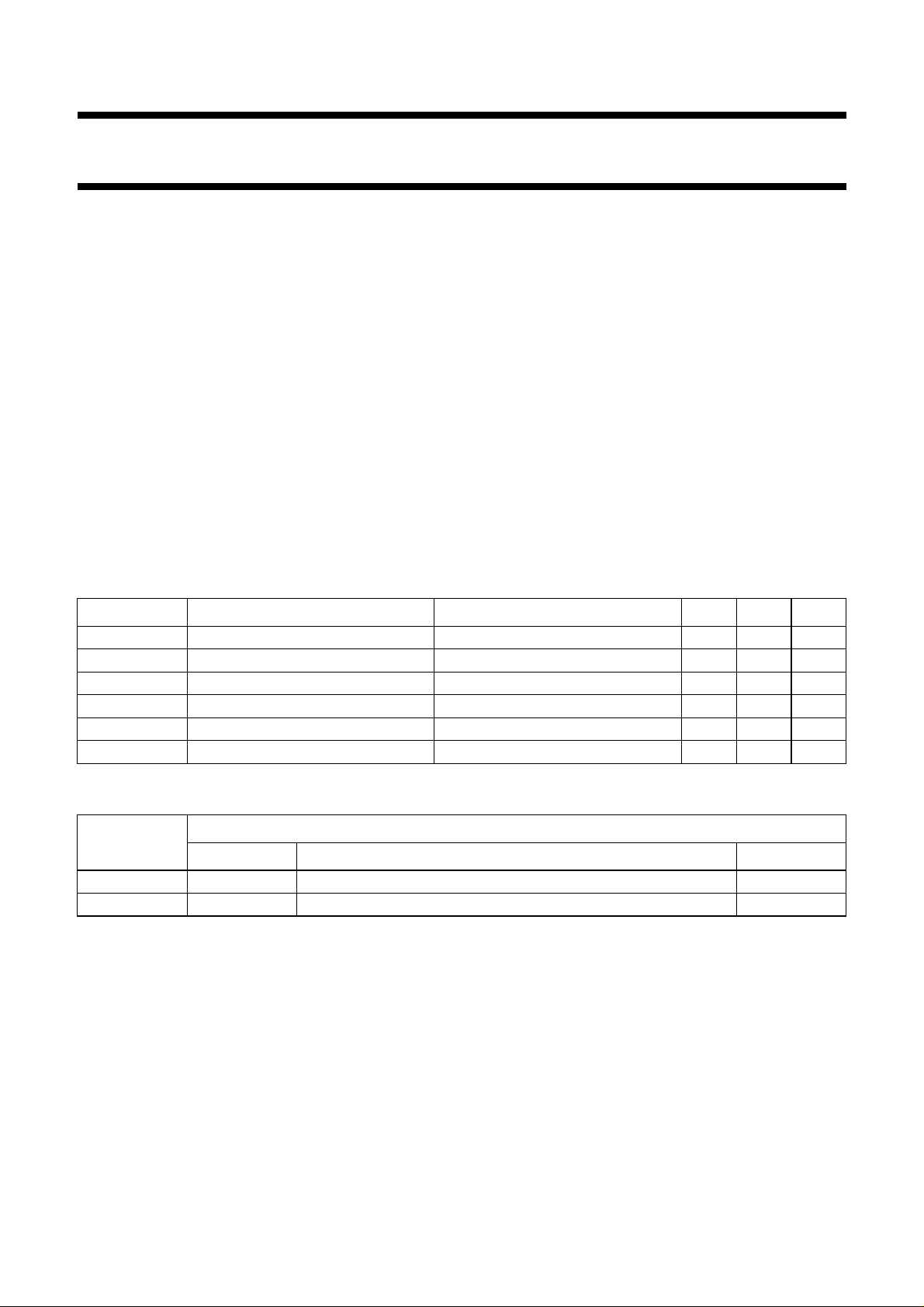
SYMBOL PARAMETER CONDITIONS MIN. MAX. UNIT
V
CC
V
CANH
V
CANL
V
i(dif)(bus)
t
PD(TXD-RXD)
T
vj
supply voltage 4.75 5.25 V
DC voltage at pin CANH 0 < VCC< 5.25 V; no time limit −27 +40 V
DC voltage at pin CANL 0 < VCC< 5.25 V; no time limit −27 +40 V
differential bus input voltage dominant 1.5 3 V
propagation delay TXD to RXD VS= 0 V; see Fig.7 − 250 ns
virtual junction temperature −40 +150 °C
ORDERING INFORMATION
TYPE
NUMBER
NAME DESCRIPTION VERSION
PACKAGE
TJA1050T SO8 plastic small outline package; 8 leads; body width 3.9 mm SOT96-1
TJA1050U − bare die; die dimensions 1700 × 1280 × 380 µm −
2003 Oct 22 2
Page 3
Philips Semiconductors Product specification
High speed CAN transceiver TJA1050
BLOCK DIAGRAM
handbook, full pagewidth
TXD
RXD
V
ref
V
CC
0.5V
CC
GND
3
GND
2
7
25
kΩ
25
kΩ
6
MGS374
CANH
CANL
8
S
30 µA
V
CC
1
4
5
200
µA
V
CC
GND
GND
TXD
DOMINANT
TIME-OUT
TIMER
REFERENCE
VOLTAGE
TEMPERATURE
PROTECTION
DRIVER
RECEIVER
TJA1050
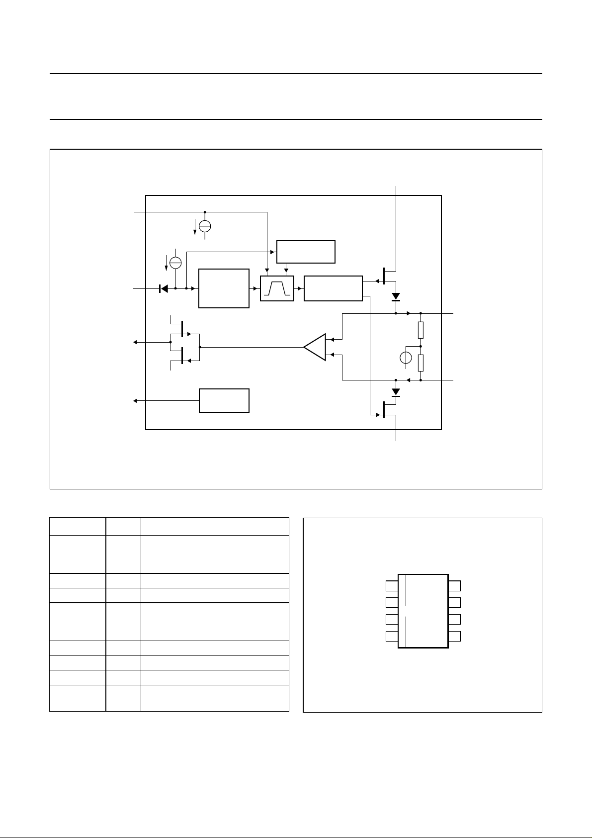
Fig.1 Block diagram.
PINNING
SYMBOL PIN DESCRIPTION
TXD 1 transmit data input; reads in data
from the CAN controller to the bus
line drivers
GND 2 ground
V
CC
3 supply voltage
RXD 4 receive data output; reads out
data from the bus lines to the
CAN controller
V
ref
5 reference voltage output
CANL 6 LOW-level CAN bus line
CANH 7 HIGH-level CAN bus line
S 8 select input for high-speed mode
or silent mode
handbook, halfpage
TXD
1
2
TJA1050T
3
V
CC
4
RXD
MGS375
Fig.2 Pin configuration.
8
7
6
5
S
CANHGND
CANL
V
ref
2003 Oct 22 3
Page 4

Philips Semiconductors Product specification
High speed CAN transceiver TJA1050
FUNCTIONAL DESCRIPTION
The TJA1050 is the interface between the CAN protocol
controller and the physical bus. It is primarily intended for
high-speed automotive applicationsusing baud rates from
60 kbaud up to 1 Mbaud. It provides differential transmit
capability to the bus and differential receiver capability to
the CAN protocol controller. It is fully compatible to the
“ISO 11898”
standard.
A current-limiting circuit protects the transmitter output
stage from damage caused by accidental short-circuit to
either positive or negative supply voltage, although power
dissipation increases during this fault condition.
A thermal protection circuit protects the IC from damage
by switching off the transmitter if the junction temperature
exceeds a value of approximately 165 °C. Because the
transmitter dissipates most of the power, the power
dissipation and temperature of the IC is reduced. All other
IC functions continue to operate. The transmitter off-state
resets when pin TXD goes HIGH. The thermal protection
circuit is particularly needed when a bus line short-circuits.
The pins CANH and CANL are protected from automotive
electrical transients (according to
“ISO 7637”
; see Fig.4).
Control pin S allows two operating modes to be selected:
high-speed mode or silent mode.
Thehigh-speed mode isthe normal operating modeand is
selected by connecting pin S to ground. It is the default
mode if pin S is not connected. However, to ensure EMI
performance in applications using only the high-speed
mode, it is recommended that pin S is connected to
ground.
In the silent mode, the transmitter is disabled. All other
IC functions continue to operate. The silent mode is
selected by connecting pin S to VCC and can be used to
prevent network communication from being blocked, due
to a CAN controller which is out of control.
A ‘TXD dominant time-out’ timer circuit prevents the bus
linesbeing driven to apermanentdominant state (blocking
all network communication) if pin TXD is forced
permanently LOW by a hardware and/or software
application failure. The timer is triggered by a negative
edge on pin TXD. If the duration of the LOW-level on
pin TXDexceedsthe internal timer value, thetransmitteris
disabled, driving the bus into a recessive state. The timer
is reset by a positive edge on pin TXD.
Table 1 Function table of the CAN transceiver; X = don’t care
V
CC
4.75 V to 5.25 V LOW LOW (or
TXD S CANH CANL BUS STATE RXD
HIGH LOW dominant LOW
floating)
4.75 V to 5.25 V X HIGH 0.5V
4.75 V to 5.25 V HIGH (or
X 0.5V
floating)
<2 V (not powered) X X 0 V < V
2V<V
< 4.75 V >2 V X 0 V < V
CC
CANH<VCC
CANH<VCC
CC
CC
0.5V
0.5V
0V<V
0V<V
CC
CC
CANL<VCC
CANL<VCC
recessive HIGH
recessive HIGH
recessive X
recessive X
2003 Oct 22 4
Page 5
Philips Semiconductors Product specification
High speed CAN transceiver TJA1050
LIMITING VALUES
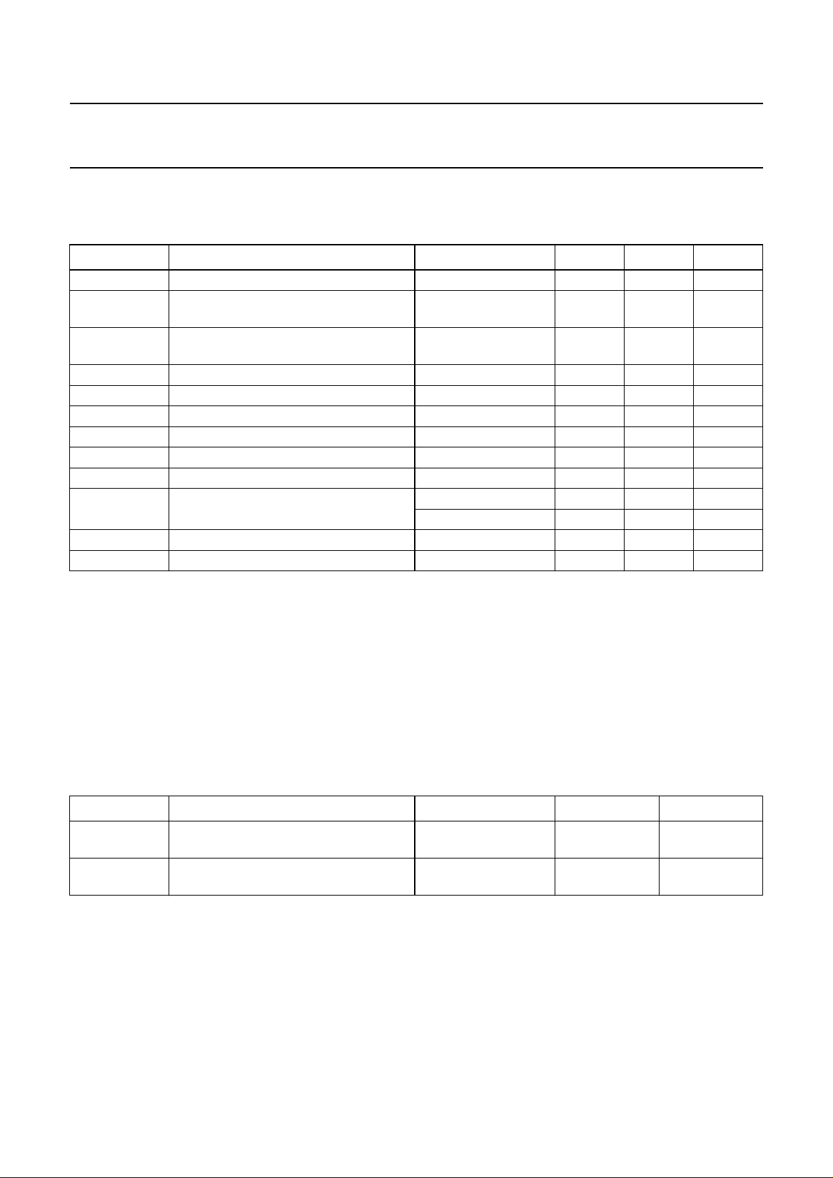
In accordance with the Absolute Maximum Rating System (IEC 60134). All voltages are referenced to GND (pin 2).
Positive currents flow into the IC.
SYMBOL PARAMETER CONDITIONS MIN. MAX. UNIT
V
CC
V
CANH
V
CANL
V
TXD
V
RXD
V
ref
V
S
V
trt(CANH)
V
trt(CANL)
V
esd
T
stg
T
vj
supply voltage −0.3 +6 V
DC voltage at pin CANH 0 < VCC< 5.25 V;
−27 +40 V
no time limit
DC voltage at pin CANL 0 < VCC< 5.25 V;
−27 +40 V
no time limit
DC voltage at pin TXD −0.3 VCC+ 0.3 V
DC voltage at pin RXD −0.3 VCC+ 0.3 V
DC voltage at pin V
ref
−0.3 VCC+ 0.3 V
DC voltage at pin S −0.3 VCC+ 0.3 V
transient voltage at pin CANH note 1 −200 +200 V
transient voltage at pin CANL note 1 −200 +200 V
electrostatic discharge voltage at all pins note 2 −4000 +4000 V
note 3 −200 +200 V
storage temperature −55 +150 °C
virtual junction temperature note 4 −40 +150 °C
Notes
1. The waveforms of the applied transients shall be in accordance with
“ISO 7637 part 1”
, test pulses 1, 2, 3a and 3b
(see Fig.4).
2. Human body model: C = 100 pF and R = 1.5 kΩ.
3. Machine model: C = 200 pF, R = 10 Ω and L = 0.75 µH.
4. In accordance with
“IEC 60747-1”
. An alternative definition of Tvjis: Tvj=T
amb
+P×R
th(vj-a)
, where R
th(vj-a)
value to be used for the calculation of Tvj. The rating for Tvjlimits the allowable combinations of power dissipation (P)
and ambient temperature (T
amb
).
THERMAL CHARACTERISTICS
According to IEC 60747-1.
SYMBOL PARAMETER CONDITIONS VALUE UNIT
R
th(vj-a)
thermal resistance from junction to
in free air 145 K/W
ambient in SO8 package
R
th(vj-s)
thermal resistance from junction to
in free air 50 K/W
substrate of bare die
QUALITY SPECIFICATION
Quality specification
“SNW-FQ-611 part D”
is applicable.
is a fixed
2003 Oct 22 5
Page 6
Philips Semiconductors Product specification
High speed CAN transceiver TJA1050
CHARACTERISTICS
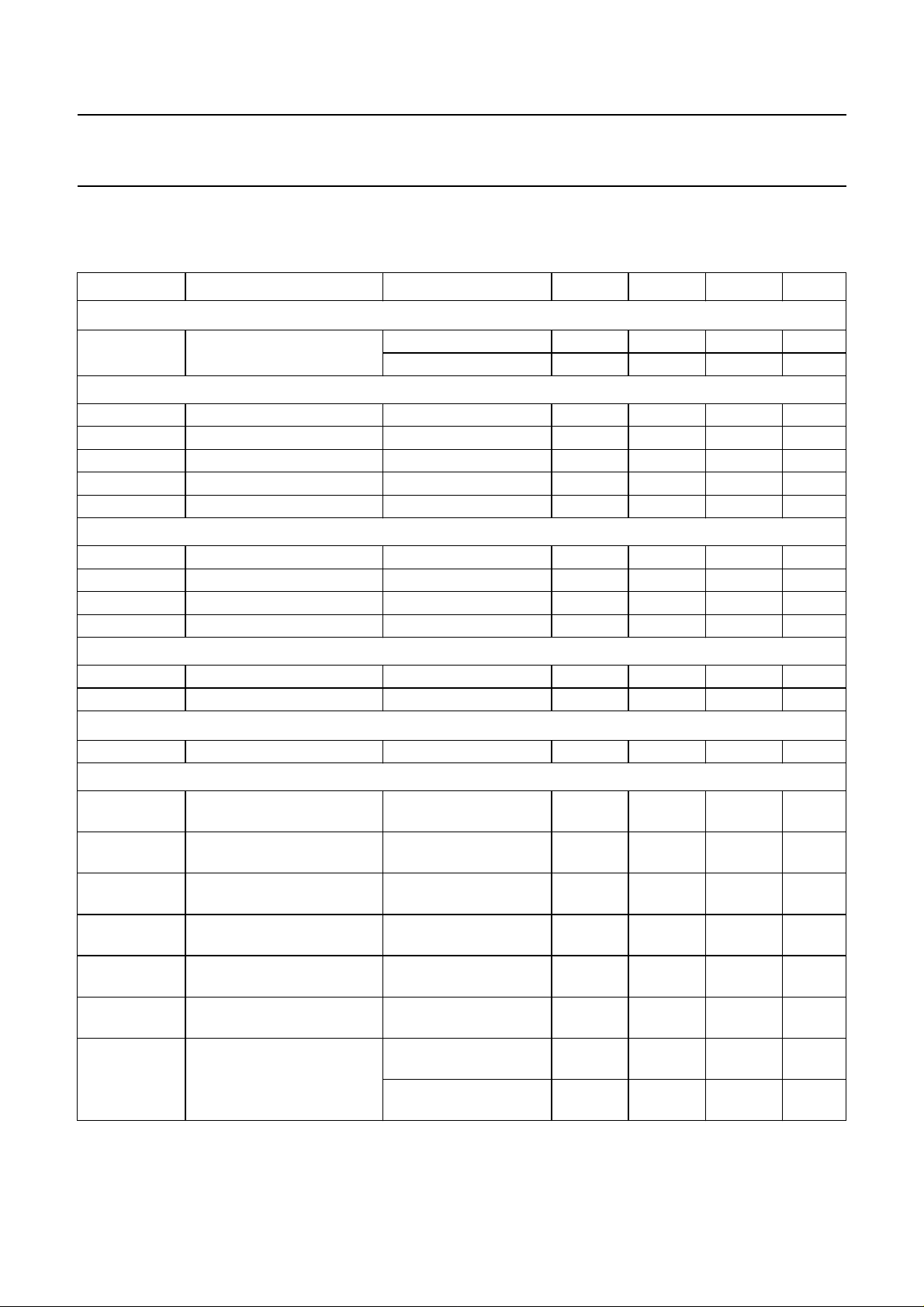
VCC= 4.75 V to 5.25 V; Tvj= −40 °C to +150 °C; RL=60Ω unless specified otherwise; all voltages are referenced to
GND (pin 2); positive currents flow into the IC; see notes 1 and 2.
SYMBOL PARAMETER CONDITIONS MIN. TYP. MAX. UNIT
Supply (pin V
I
CC
)
CC
supply current dominant; V
Transmitter data input (pin TXD)
V
IH
V
IL
I
IH
I
IL
C
i
HIGH-level input voltage output recessive 2.0 − VCC+ 0.3 V
LOW-level input voltage output dominant −0.3 − +0.8 V
HIGH-level input current V
LOW-level input current V
input capacitance not tested − 510pF
Mode select input (pin S)
V
IH
V
IL
I
IH
I
IL
HIGH-level input voltage silent mode 2.0 − VCC+ 0.3 V
LOW-level input voltage high-speed mode −0.3 − +0.8 V
HIGH-level input current VS= 2 V 20 30 50 µA
LOW-level input current VS=0.8V 153045µA
Receiver data output (pin RXD)
I
OH
I
OL
HIGH-level output current V
LOW-level output current V
Reference voltage output (pin V
V
ref
reference output voltage −50 µA<I
Bus lines (pins CANH and CANL)
V
o(reces)(CANH)
recessive bus voltage at
pin CANH
V
o(reces)(CANL)
recessive bus voltage at
pin CANL
I
o(reces)(CANH)
recessive output current at
pin CANH
I
o(reces)(CANL)
recessive output current at
pin CANL
V
o(dom)(CANH)
dominant output voltage at
pin CANH
V
o(dom)(CANL)
dominant output voltage at
pin CANL
V
i(dif)(bus)
differential bus input voltage
(V
CANH
− V
CANL
)
ref
=0V255075mA
TXD
recessive; V
TXD=VCC
TXD
RXD
RXD
TXD=VCC
=0V −100 −200 −300 µA
= 0.7V
CC
= 0.45 V 2 8.5 20 mA
2.5 5 10 mA
−50 +5µA
−2 −6 −15 mA
)
V
TXD=VCC
V
TXD=VCC
−27V<V
< +50 µA 0.45V
Vref
; no load 2.0 2.5 3.0 V
; no load 2.0 2.5 3.0 V
CANH
< +32 V;
−2.0 − +2.5 mA
CC
0.5V
CC
0.55V
CC
V
0V<VCC< 5.25 V
−27V<V
CANL
< +32 V;
−2.0 − +2.5 mA
0V<VCC< 5.25 V
V
= 0 V 3.0 3.6 4.25 V
TXD
V
= 0 V 0.5 1.4 1.75 V
TXD
V
= 0 V; dominant;
TXD
1.5 2.25 3.0 V
42.5 Ω <RL<60Ω
V
TXD=VCC
; recessive;
−50 0 +50 mV
no load
2003 Oct 22 6
Page 7
Philips Semiconductors Product specification
High speed CAN transceiver TJA1050
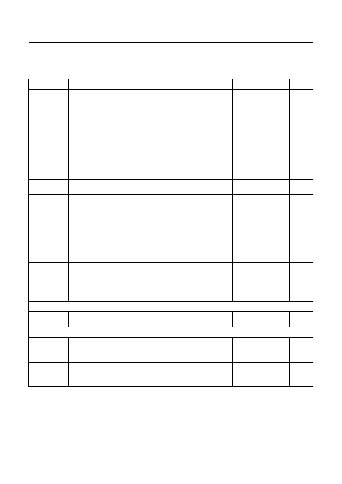
SYMBOL PARAMETER CONDITIONS MIN. TYP. MAX. UNIT
I
o(sc)(CANH)
I
o(sc)(CANL)
V
i(dif)(th)
V
i(dif)(hys)
R
i(cm)(CANH)
R
i(cm)(CANL)
R
i(cm)(m)
R
i(dif)
C
i(CANH)
C
i(CANL)
C
i(dif)
I
LI(CANH)
I
LI(CANL)
Thermal shutdown
T
j(sd)
Timing characteristics (see Figs.6 and 7)
t
d(TXD-BUSon)
t
d(TXD-BUSoff)
t
d(BUSon-RXD)
t
d(BUSoff-RXD)
t
dom(TXD)
short-circuit output currentat
V
CANH
=0V;V
=0V −45 −70 −95 mA
TXD
pin CANH
short-circuit output currentat
pin CANL
differentialreceiverthreshold
voltage
V
=36V;
CANL
V
=0V
TXD
−12V<V
−12V<V
CANL
CANH
< +12 V;
< +12 V;
45 70 100 mA
0.5 0.7 0.9 V
see Fig.5
differential receiver input
voltage hysteresis
−12V<V
−12V<V
CANL
CANH
< +12 V;
< +12 V;
50 70 100 mV
see Fig.5
common mode input
15 25 35 kΩ
resistance at pin CANH
common mode input
15 25 35 kΩ
resistance at pin CANL
matching between
V
CANH=VCANL
−3 0 +3 %
pin CANH and pin CANL
common mode input
resistance
differential input resistance 25 50 75 kΩ
input capacitance at
V
TXD=VCC
; not tested − 7.5 20 pF
pin CANH
input capacitance at
V
TXD=VCC
; not tested − 7.5 20 pF
pin CANL
differential input capacitance V
input leakage current at
TXD=VCC
VCC=0V; V
; not tested − 3.75 10 pF
= 5 V 100 170 250 µA
CANH
pin CANH
input leakage current at
VCC=0V; V
= 5 V 100 170 250 µA
CANL
pin CANL
shutdown junction
155 165 180 °C
temperature
delay TXD to bus active VS= 0 V 25 55 110 ns
delay TXD to bus inactive VS= 0 V 25 60 95 ns
delay bus active to RXD VS= 0 V 20 50 110 ns
delay bus inactive to RXD VS= 0 V 45 95 155 ns
TXD dominant time for
V
= 0 V 250 450 750 µs
TXD
time-out
Notes
1. Allparameters are guaranteed overthevirtual junctiontemperaturerange by design, butonly100 % tested at125 °C
ambient temperature for dies on wafer level and in addition to this 100 % tested at 25 °C ambient temperature for
cased products, unless specified otherwise.
2. For bare die, all parameters are only guaranteed if the backside of the bare die is connected to ground.
2003 Oct 22 7
Page 8
Philips Semiconductors Product specification
High speed CAN transceiver TJA1050
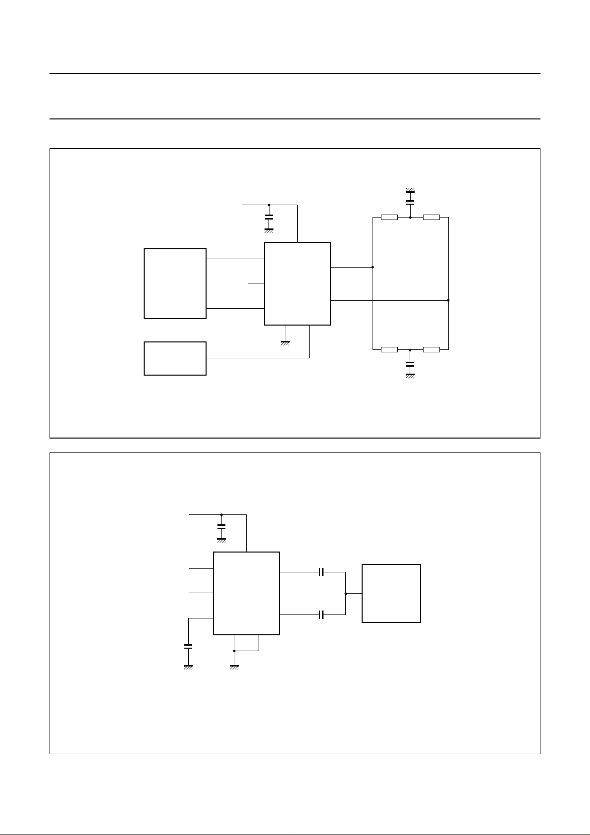
APPLICATION AND TEST INFORMATION
handbook, full pagewidth
47 nF
60 Ω
CAN
BUS LINE
60 Ω
47 nF
MGS380
TX0
SJA1000
CAN
CONTROLLER
RX0
MICRO-
CONTROLLER
+
5 V
TXD
V
ref
RXD
100
nF
1
5
4
V
CC
3
TJA1050
GND S
60 Ω
CANH
7
CANL
6
82
60 Ω
handbook, full pagewidth
Fig.3 Application information.
+
5 V
TXD
V
RXD
15 pF
ref
100
nF
1
5
4
V
CC
3
TJA1050
GND S
CANH
7
CANL
6
82
1 nF
1 nF
TRANSIENT
GENERATOR
MGS379
The waveforms of the applied transients shall be in accordance with
“ISO 7637 part 1”
Fig.4 Test circuit for automotive transients.
2003 Oct 22 8
, test pulses 1, 2, 3a and 3b.
Page 9
Philips Semiconductors Product specification
High speed CAN transceiver TJA1050
handbook, full pagewidth
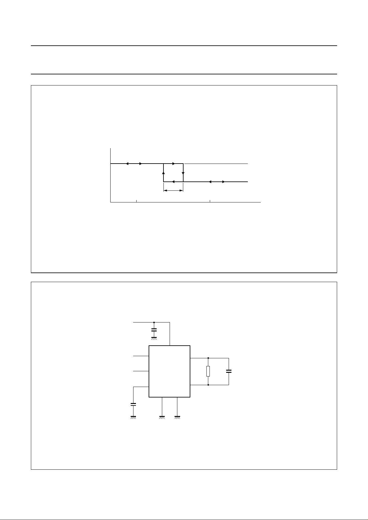
V
RXD
0.5 0.9
+
5 V
handbook, halfpage
TXD
V
RXD
15 pF
hysteresis
Fig.5 Hysteresis of the receiver.
100
nF
V
CC
ref
1
5
4
3
TJA1050
GND S
CANH
7
R
L
60 Ω
CANL
6
82
V
i(dif)(bus)
C
L
100 pF
MGS378
HIGH
LOW
(V)
Fig.6 Test circuit for timing characteristics.
2003 Oct 22 9
MGS376
Page 10
Philips Semiconductors Product specification
High speed CAN transceiver TJA1050
handbook, full pagewidth
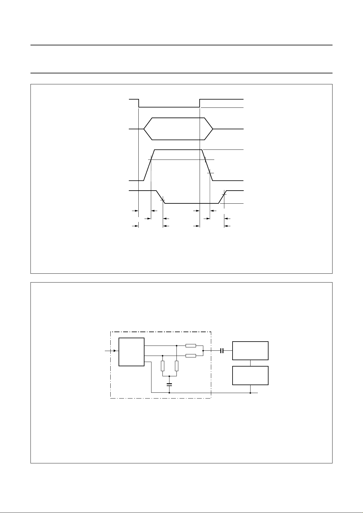
(1) V
i(dif)(bus)=VCANH
− V
CANL
.
TXD
CANH
CANL
V
i(dif)(bus)
RXD
t
d(TXD-BUSon)
t
d(BUSon-RXD)
0.9 V
(1)
0.5 V
0.7V
t
d(TXD-BUSoff)
t
d(BUSoff-RXD)
)
t
PD(TXD-RXD
0.3V
)
CC
t
PD(TXD-RXD
Fig.7 Timing diagram for AC characteristics.
HIGH
LOW
dominant
(BUS on)
recessive
(BUS off)
HIGH
CC
LOW
MGS377
handbook, full pagewidth
6.2 kΩ
6.2 kΩ
30
30
Ω
Ω
47 nF
10 nF
ACTIVE PROBE
SPECTRUM-
ANALYZER
GND
MGT229
TX
TJA1050
test PCB
CANL
CANH
Fig.8 Basic test set-up (with split termination) for electromagnetic emission measurement (see Figs 9 and 10).
2003 Oct 22 10
Page 11
Philips Semiconductors Product specification
High speed CAN transceiver TJA1050
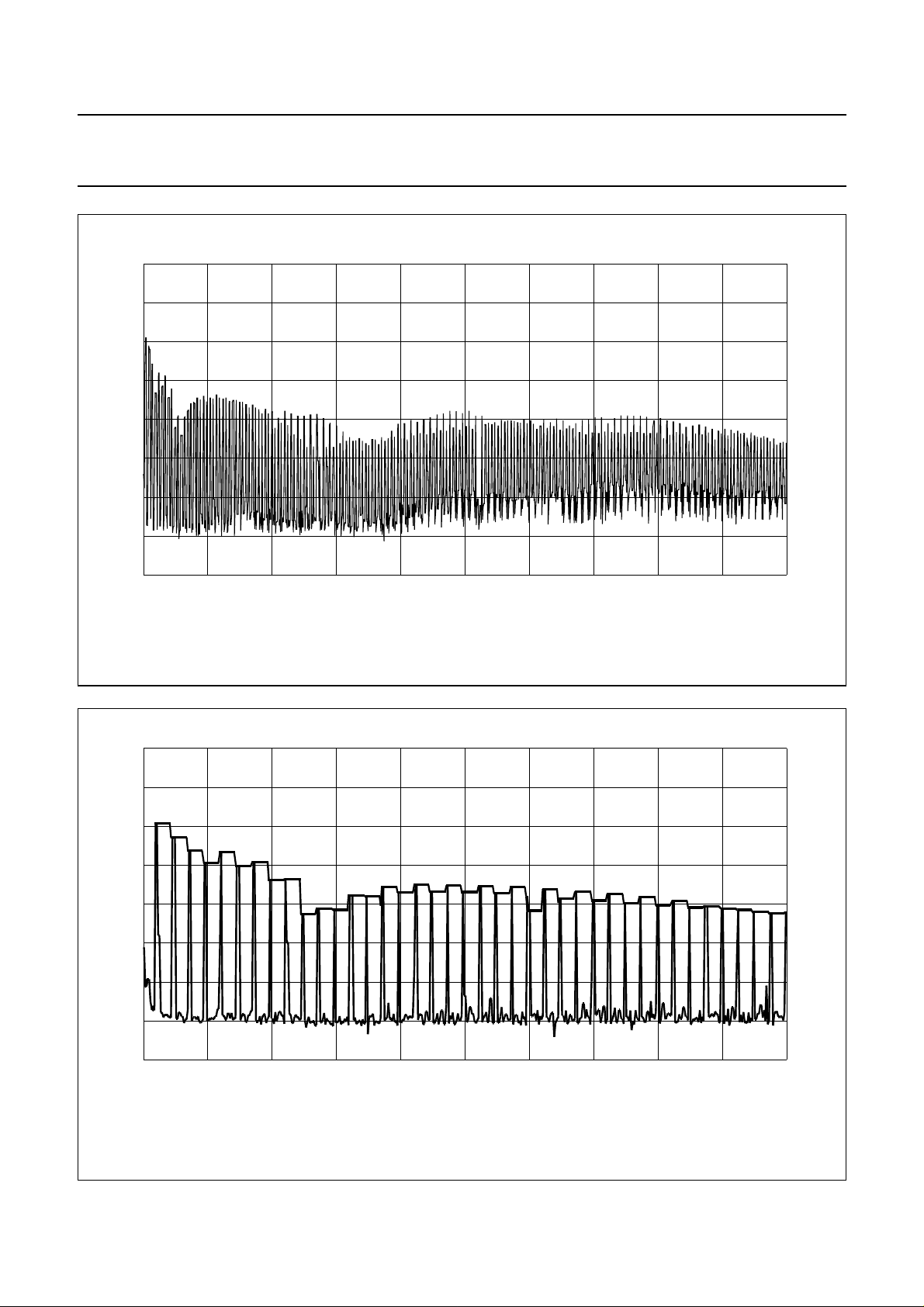
80
handbook, full pagewidth
A
(dBµV)
60
40
20
0
0203010
Data rate of 500 kbits/s.
40
f (MHz)
Fig.9 Typical electromagnetic emission up to 50 MHz (peak amplitude measurement).
MGT231
50
80
handbook, full pagewidth
A
(dBµV)
60
40
20
0
0462
Data rate of 500 kbits/s.
8
f (MHz)
MGT233
Fig.10 Typical electromagnetic emission up to 10 MHz (peak amplitude measurement and envelope on peak
amplitudes).
10
2003 Oct 22 11
Page 12
Philips Semiconductors Product specification
High speed CAN transceiver TJA1050
handbook, full pagewidth
30 Ω
30 Ω
4.7 nF
test PCB
MGT230
RF VOLTMETER
AND POWER
AMPLIFIER
50
RF SIGNAL
Ω
GENERATOR
GND
TX
RX
TJA1050
TJA1050
CANL
CANH
30
handbook, full pagewidth
V
RF(rms)
(V)
max RF voltage reached with no errors
20
10
0
−1
10
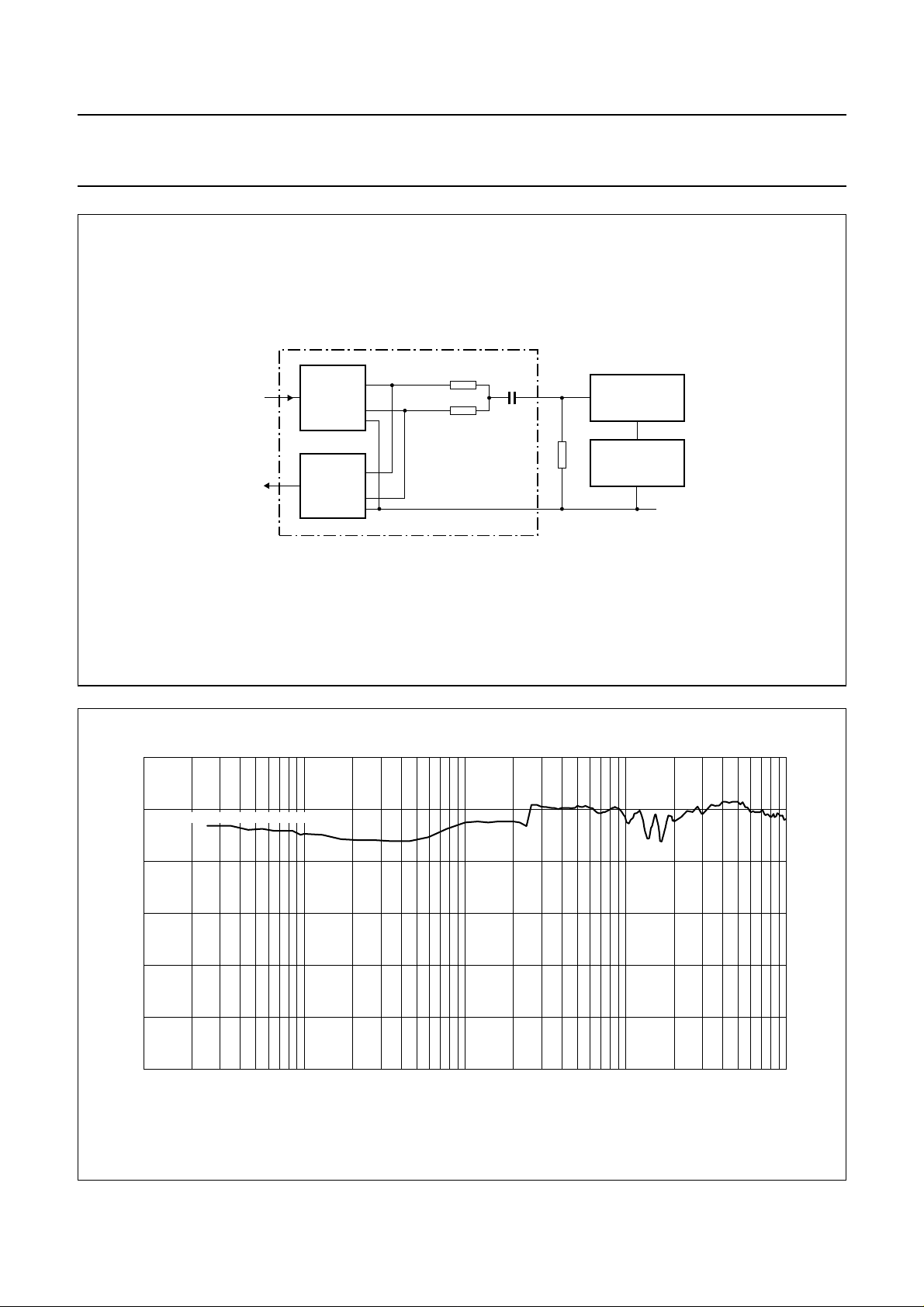
Fig.11 Basic test set-up for electromagnetic immunity measurement (see Fig.12).
2
101
10
f (MHz)
MGT232
3
10
Data rate of 500 kbits/s.
Fig.12 Typical electromagnetic immunity.
2003 Oct 22 12
Page 13
Philips Semiconductors Product specification
High speed CAN transceiver TJA1050
BONDING PAD LOCATIONS
COORDINATES
(1)
SYMBOL PAD
xy
TXD 1 103 103
GND 2 740 85
V
CC
3 886.5 111
RXD 4 1371.5 111
V
ref
5 1394 1094
CANL 6 998 1115
CANH 7 538.5 1115
S 8 103 1097
Note
1. All x/y coordinates represent the position of the centre
ofeach pad (in µm) withrespect to the lefthandbottom
corner of the top aluminium layer (see Fig.13).
8
handbook, halfpage
x
0
0
y
The backside of the bare die must be connected to ground.
765
TJA1050U
1
23 4
MGS381
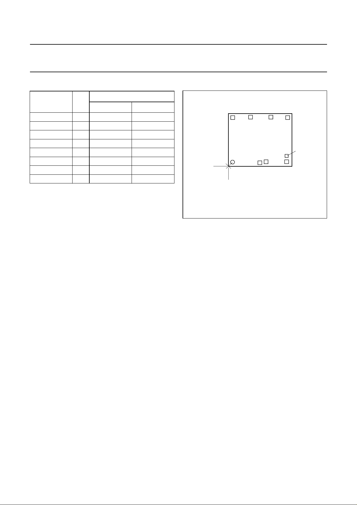
Fig.13 Bonding pad locations.
test pad
2003 Oct 22 13
Page 14
Philips Semiconductors Product specification
High speed CAN transceiver TJA1050
PACKAGE OUTLINE
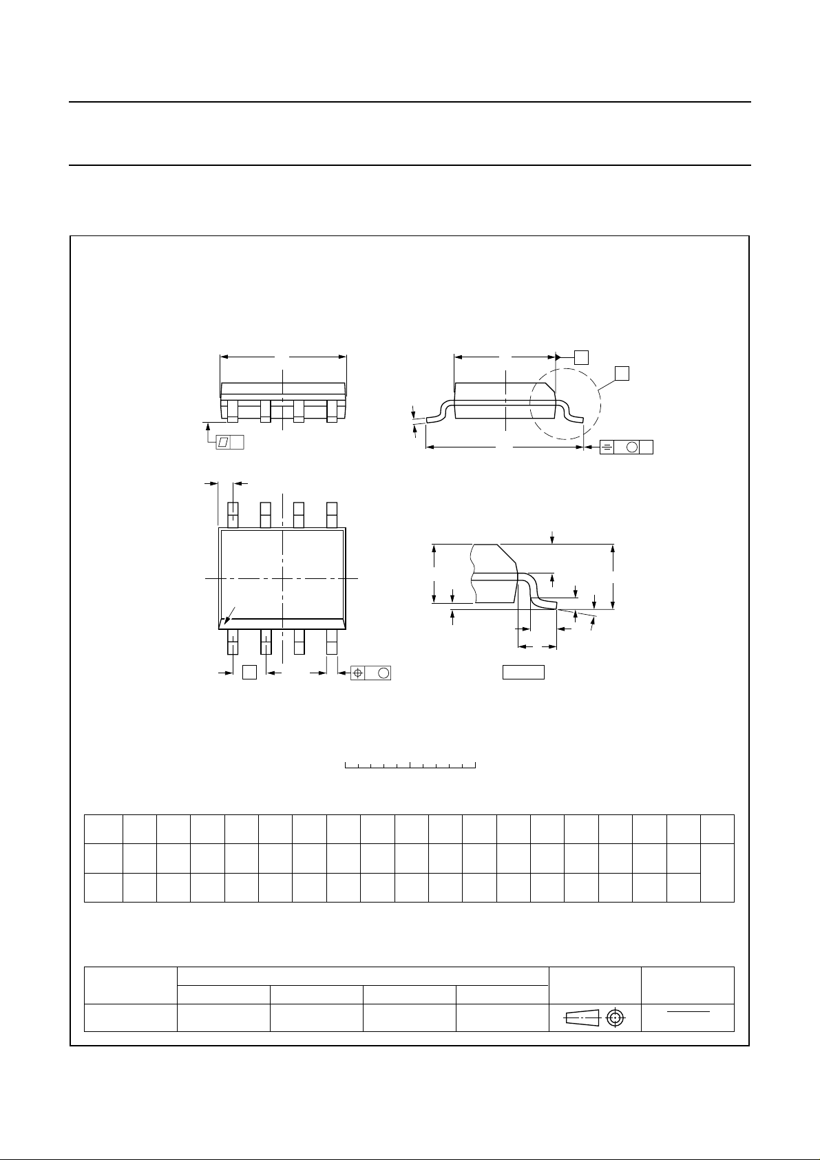
SO8: plastic small outline package; 8 leads; body width 3.9 mm
D
c
y
Z
8
pin 1 index
1
e
5
A
2
A
4
w M
b
p
SOT96-1
E
H
E
1
L
detail X
A
X
v M
A
Q
(A )
L
p
A
3
θ
0 2.5 5 mm
scale
DIMENSIONS (inch dimensions are derived from the original mm dimensions)
mm
OUTLINE
VERSION
SOT96-1
A
max.
1.75
0.069
A
0.25
0.10
0.010
0.004
A2A
1
1.45
1.25
0.057
0.049
IEC JEDEC JEITA
076E03 MS-012
0.25
0.01
b
3
p
0.49
0.25
0.36
0.19
0.019
0.0100
0.014
0.0075
UNIT
inches
Notes
1. Plastic or metal protrusions of 0.15 mm (0.006 inch) maximum per side are not included.
2. Plastic or metal protrusions of 0.25 mm (0.01 inch) maximum per side are not included.
(1)E(2)
cD
5.0
4.8
0.20
0.19
REFERENCES
eHELLpQZywv θ
4.0
1.27
3.8
0.16
0.05
0.15
2003 Oct 22 14
6.2
5.8
0.244
0.228
1.05
1.0
0.4
0.039
0.016
0.7
0.6
0.028
0.024
0.25 0.10.25
0.010.010.041 0.004
EUROPEAN
PROJECTION
(1)
0.7
0.3
0.028
0.012
ISSUE DATE
99-12-27
03-02-18
o
8
o
0
Page 15

Philips Semiconductors Product specification
High speed CAN transceiver TJA1050
SOLDERING
Introduction to soldering surface mount packages
Thistextgives a very brief insighttoacomplex technology.
A more in-depth account of soldering ICs can be found in
our
“Data Handbook IC26; Integrated Circuit Packages”
(document order number 9398 652 90011).
There is no soldering method that is ideal for all surface
mount IC packages. Wave soldering can still be used for
certainsurfacemount ICs, but it is not suitableforfinepitch
SMDs. In these situations reflow soldering is
recommended.
Reflow soldering
Reflow soldering requires solder paste (a suspension of
fine solder particles, flux and binding agent) to be applied
tothe printed-circuit board byscreenprinting, stencilling or
pressure-syringe dispensing before package placement.
Driven by legislation and environmental forces the
worldwide use of lead-free solder pastes is increasing.
Several methods exist for reflowing; for example,
convection or convection/infrared heating in a conveyor
type oven. Throughput times (preheating, soldering and
cooling) vary between 100 and 200 seconds depending
on heating method.
Typical reflow peak temperatures range from
215 to 270 °C depending on solder paste material. The
top-surface temperature of the packages should
preferably be kept:
• below 220 °C (SnPb process) or below 245 °C (Pb-free
process)
– for all BGA and SSOP-T packages
– for packages with a thickness ≥ 2.5 mm
– for packages with a thickness < 2.5 mm and a
volume ≥ 350 mm3 so called thick/large packages.
• below 235 °C (SnPb process) or below 260 °C (Pb-free
process) for packages with a thickness < 2.5 mm and a
volume < 350 mm3 so called small/thin packages.
Moisture sensitivity precautions, as indicated on packing,
must be respected at all times.
If wave soldering is used the following conditions must be
observed for optimal results:
• Use a double-wave soldering method comprising a
turbulent wave with high upward pressure followed by a
smooth laminar wave.
• For packages with leads on two sides and a pitch (e):
– larger than or equal to 1.27 mm, the footprint
longitudinal axis is preferred to be parallel to the
transport direction of the printed-circuit board;
– smaller than 1.27 mm, the footprint longitudinal axis
must be parallel to the transport direction of the
printed-circuit board.
The footprint must incorporate solder thieves at the
downstream end.
• Forpackageswith leads on four sides, the footprintmust
be placed at a 45° angle to the transport direction of the
printed-circuit board. The footprint must incorporate
solder thieves downstream and at the side corners.
During placement andbefore soldering, the package must
be fixed with a droplet of adhesive. The adhesive can be
applied by screen printing, pin transfer or syringe
dispensing. The package can be soldered after the
adhesive is cured.
Typical dwell time of the leads in the wave ranges from
3 to 4 seconds at 250 °C or 265 °C, depending on solder
material applied, SnPb or Pb-free respectively.
A mildly-activated flux will eliminate the need for removal
of corrosive residues in most applications.
Manual soldering
Fix the component by first soldering two
diagonally-opposite end leads. Use a low voltage (24 V or
less) soldering iron applied to the flat part of the lead.
Contact time must be limited to 10 seconds at up to
300 °C.
When using a dedicated tool, all other leads can be
soldered in one operation within 2 to 5 seconds between
270 and 320 °C.
Wave soldering
Conventional single wave soldering is not recommended
forsurfacemount devices (SMDs) or printed-circuit boards
with a high component density, as solder bridging and
non-wetting can present major problems.
To overcome these problems the double-wave soldering
method was specifically developed.
2003 Oct 22 15
Page 16

Philips Semiconductors Product specification
High speed CAN transceiver TJA1050
Suitability of surface mount IC packages for wave and reflow soldering methods
PACKAGE
BGA, LBGA, LFBGA, SQFP, SSOP-T
(1)
(3)
, TFBGA, VFBGA not suitable suitable
DHVQFN, HBCC, HBGA, HLQFP, HSQFP, HSOP, HTQFP,
not suitable
SOLDERING METHOD
WAVE REFLOW
(4)
suitable
(2)
HTSSOP, HVQFN, HVSON, SMS
(5)
PLCC
LQFP, QFP, TQFP not recommended
SSOP, TSSOP, VSO, VSSOP not recommended
PMFP
, SO, SOJ suitable suitable
(5)(6)
suitable
(7)
suitable
(8)
not suitable not suitable
Notes
1. Formore detailed information on theBGA packages refer to the
“(LF)BGAApplication Note
”(AN01026); order a copy
from your Philips Semiconductors sales office.
2. All surface mount (SMD) packages are moisture sensitive. Depending upon the moisture content, the maximum
temperature (with respect to time) and body size of the package, there is a risk that internal or external package
cracks may occur due to vaporization of the moisture in them (the so called popcorn effect). For details, refer to the
Drypack information in the
“Data Handbook IC26; Integrated Circuit Packages; Section: Packing Methods”
.
3. These transparent plastic packages are extremely sensitive to reflow soldering conditions and must on no account
be processed through more than one soldering cycle or subjected to infrared reflow soldering with peak temperature
exceeding 217 °C ± 10 °C measured in the atmosphere of the reflow oven. The package body peak temperature
must be kept as low as possible.
4. These packages are not suitable for wave soldering. On versions with the heatsink on the bottom side, the solder
cannot penetrate between the printed-circuit board and the heatsink. On versions with the heatsink on the top side,
the solder might be deposited on the heatsink surface.
5. If wave soldering is considered, then the package must be placed at a 45° angle to the solder wave direction.
The package footprint must incorporate solder thieves downstream and at the side corners.
6. Wave soldering is suitable for LQFP, TQFP and QFP packages with a pitch (e) larger than 0.8 mm; it is definitely not
suitable for packages with a pitch (e) equal to or smaller than 0.65 mm.
7. Wave soldering is suitable for SSOP, TSSOP, VSO and VSSOP packages with a pitch (e) equal to or larger than
0.65 mm; it is definitely not suitable for packages with a pitch (e) equal to or smaller than 0.5 mm.
8. Hot bar or manual soldering is suitable for PMFP packages.
REVISION HISTORY
REV DATE CPCN DESCRIPTION
4 20031013 − Product specification (9397 750 12157)
Modification:
• Added recommendation to connect unused pin S to ground
• Added Chapter REVISION HISTORY
3 20020516 − Product specification (9397 750 09778)
2003 Oct 22 16
Page 17

Philips Semiconductors Product specification
High speed CAN transceiver TJA1050
DATA SHEET STATUS
LEVEL
DATA SHEET
STATUS
(1)
PRODUCT
STATUS
(2)(3)
DEFINITION
I Objective data Development This data sheet contains data from the objective specification for product
development. Philips Semiconductors reserves the right to change the
specification in any manner without notice.
II Preliminary data Qualification This data sheet contains data from the preliminary specification.
Supplementary data will be published at a later date. Philips
Semiconductors reserves the right to change the specification without
notice, in order to improve the design and supply the best possible
product.
III Product data Production This data sheet contains data from the product specification. Philips
Semiconductors reserves the right to make changes at any time in order
to improve the design, manufacturing and supply. Relevant changes will
be communicated via a Customer Product/Process Change Notification
(CPCN).
Notes
1. Please consult the most recently issued data sheet before initiating or completing a design.
2. The product status of the device(s) described in this data sheet may have changed since this data sheet was
published. The latest information is available on the Internet at URL http://www.semiconductors.philips.com.
3. For data sheets describing multipletype numbers, the highest-level product status determines the data sheet status.
DEFINITIONS
DISCLAIMERS
Short-form specification The data in a short-form
specification is extracted from a full data sheet with the
same type number and title. For detailed information see
the relevant data sheet or data handbook.
Limiting values definition Limiting values given are in
accordance with the Absolute Maximum Rating System
(IEC 60134). Stress above one or more of the limiting
values may cause permanent damage to the device.
These are stress ratings only and operation of the device
attheseor at any otherconditionsabovethose given in the
Characteristics sections of the specification is not implied.
Exposure to limiting values for extended periods may
affect device reliability.
Application information Applications that are
described herein for any of these products are for
illustrative purposes only. Philips Semiconductors make
norepresentationorwarrantythat such applications will be
suitable for the specified use without further testing or
modification.
Life support applications These products are not
designed for use in life support appliances, devices, or
systems where malfunction of these products can
reasonably be expected to result in personal injury. Philips
Semiconductorscustomersusingorselling these products
for use in such applications do so at their own risk and
agree to fully indemnify Philips Semiconductors for any
damages resulting from such application.
Right to make changes Philips Semiconductors
reserves the right to make changes in the products including circuits, standard cells, and/or software described or contained herein in order to improve design
and/or performance. Whenthe product is in fullproduction
(status ‘Production’), relevant changes will be
communicated via a Customer Product/Process Change
Notification (CPCN). Philips Semiconductors assumes no
responsibility or liability for the use of any of these
products, conveys no licence or title under any patent,
copyright, or mask work right to these products, and
makes no representations or warranties that these
products are free from patent, copyright, or mask work
right infringement, unless otherwise specified.
2003 Oct 22 17
Page 18

Philips Semiconductors – a w orldwide compan y
Contact information
For additional information please visit http://www.semiconductors.philips.com. Fax: +31 40 27 24825
For sales offices addresses send e-mail to: [email protected].
© Koninklijke Philips Electronics N.V. 2003
All rights are reserved. Reproduction in whole or in part is prohibited without the prior written consent of the copyright owner.
The information presented in this document does not form part of any quotation or contract, is believed to be accurate and reliable and may be changed
without notice. No liability will be accepted by the publisher for any consequence of its use. Publication thereof does not convey nor imply any license
under patent- or other industrial or intellectual property rights.
Printed in The Netherlands R16/04/pp18 Date of release: 2003 Oct 22 Document order number: 9397 750 12157
SCA75
 Loading...