

Philips TEA6824T Datasheet

INTEGRATED CIRCUITS
DATA SH EET
TEA6824T
In Car Entertainment (ICE) car
radio
Preliminary specification
Supersedes data of 1996 Nov 04
File under Integrated Circuits, IC01
1997 May 05

Philips Semiconductors Preliminary specification
In Car Entertainment (ICE) car radio TEA6824T
FEATURES
• FM mixer for conversion from FM-IF1= 72.2 MHz to
FM-IF2= 10.7 MHz
• AM mixer for conversion from AM-IF1= 10.7 MHz to
AM-IF2= 450 kHz
• FM-IF gain stage
• Crystal oscillator providing mixer frequencies and
references for IF-counter
• FM quadrature demodulator with automatic centre
frequency adjustment and THD compensation
• AM-IF-amplifier and demodulator
2
C-bus transceiver with interface to enable direct data
• I
transfer to radio front-end
• IF-count for AM and FM
• Analog-to-digital conversion of level voltage and
multi-path information
• Reference frequency generation for PLL synthesizer.
GENERAL DESCRIPTION
The TEA6824T together with the TEA6810T forms the
receiver part of an AM/FM electronically tuned car radio
providing FM MPX signal and AM AF signal for Car Digital
Signal Processor (CDSP) applications.
ORDERING INFORMATION
TYPE NUMBER
NAME DESCRIPTION VERSION
TEA6824T VSO56 plastic very small outline package; 56 leads; face down SOT190-2
PACKAGE
1997 May 05 2
Philips Semiconductors Preliminary specification
In Car Entertainment (ICE) car radio TEA6824T
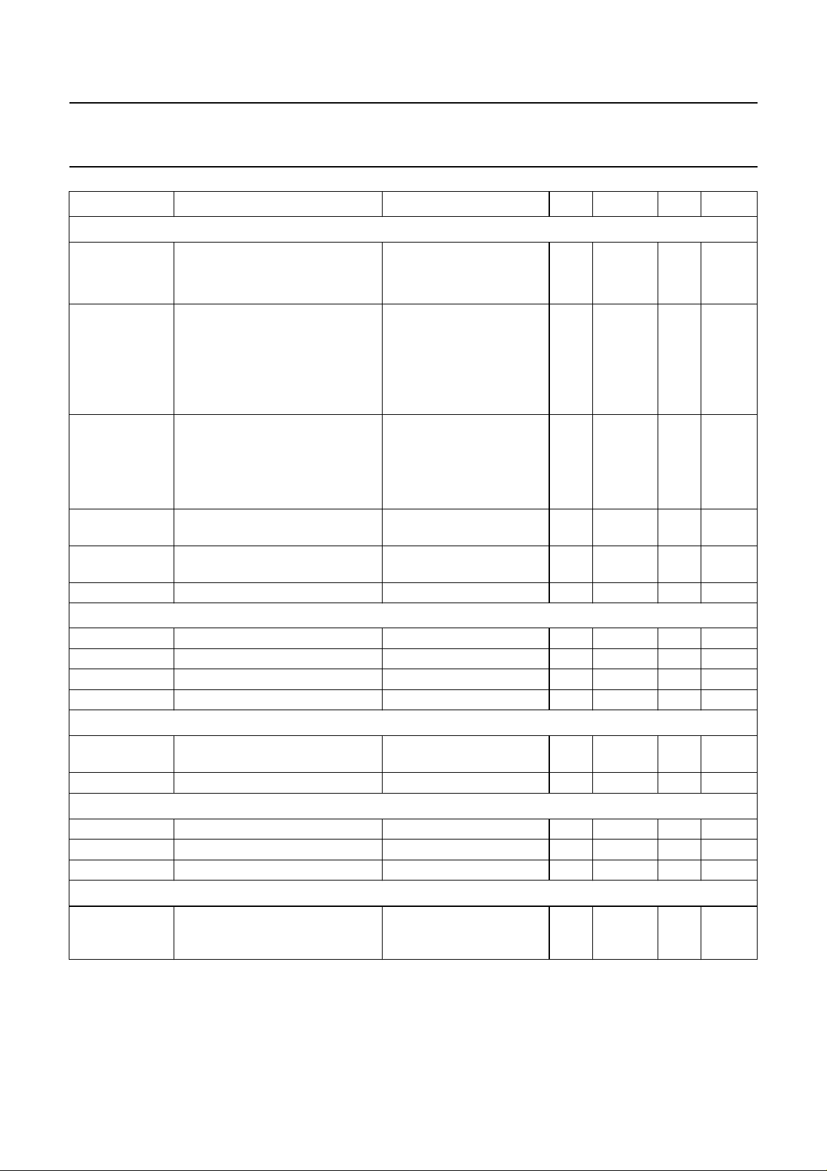
QUICK REFERENCE DATA
SYMBOL PARAMETER CONDITIONS MIN. TYP. MAX. UNIT
V
DDA1
I
DDA1
I
19+I20
I
22+I23
V
DDA2
I
DDA2
V
DDA3
I
DDA3
V
DDD
I
DDD
SN+
-------------N
THD total harmonic distortion FM mode; ∆f = 75 kHz − 0.1 0.35 %
T
amb
analog supply voltage 1 (+5 V; pin 5) note 1 4.5 5.0 5.5 V
operating range 4.75 5.0 5.25 V
analog supply current 1 (pin 5) FM mode 17 21 25 mA
AM mode 14 17 21 mA
total FM mixer output current
4.8 6.0 7.2 mA
(pins 19 and 20)
total AM mixer output current
10 12 14 mA
(pins 22 and 23)
analog supply voltage 2 (pin 28) note 1 7.0 8.5 10 V
operating range 8.1 8.5 8.9 V
analog supply current 2 (pin 28) FM mode 2.4 3.0 3.6 mA
analog supply voltage 3 (+8.5 V; pin 56) note 1 7.0 8.5 10 V
operating range 8.1 8.5 8.9 V
analog supply current 3 (pin 56) FM mode 19 25 31 mA
AM mode 9.5 12 15 mA
digital supply voltage 1 (+5 V; pin 5) note 1 4.5 5.0 5.5 V
operating range 4.75 5.0 5.25 V
digital supply current (pin 52) note 1 8 10 12 mA
signal plus noise-to-noise ratio FM mode;
66 75 − dB
∆f = 22.5 kHz at pin 47
AM mode; m = 0.3 54 60 − dB
AM mode − 1.5 3.0 %
operating ambient temperature −40 − +85 °C
Note
1. IC is operating; specified parameters may deviate from limits which are valid for operating range.
1997 May 05 3

Philips Semiconductors Preliminary specification
h
In Car Entertainment (ICE) car radio TEA6824T
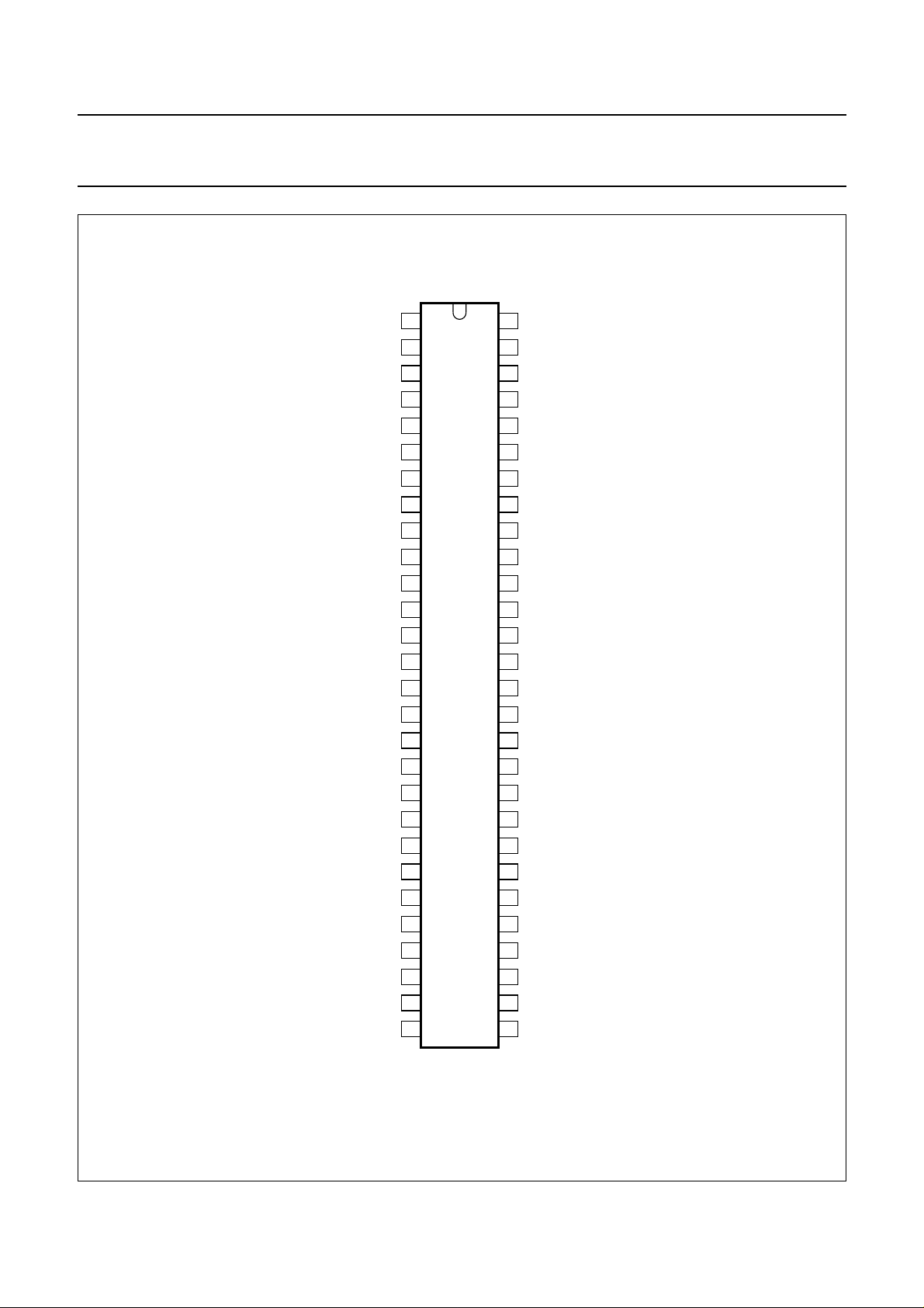
BLOCK DIAGRAM
7PSAG-1946D = S
V
CC1
10.7 MHz
SFE10.7
330 Ω
10.7 MHz
10.7 MHz
10.7 MHz
ZS369SCS-2144AJ
72.2 MHz
100 nF
22 nF
100 nF
56 pF
61.5 MHz
PHILIPS
9922 521 00098
or Daiwa AT - 49
f
ref
SDA
10 kΩ
SCL
10 kΩ
V
CCD
+5 V
TR3
10
nF
TR5
22 23
37
35
27
24
28
AMPLIFIER
29
19
20
13
14
8
OSCILLATOR
9
10
REFERENCE
11
FREQUENCY
6
7
AM
÷ 2 /÷ 6
IF
FM
SFP450
1.5 nF
10 kΩ
10 kΩ
FMSTOP
100
34
33
AM/FM
SWITCH
:N5
IF
COUNTER
54
V
ref
100 kΩ
R39
100 nF
nF
42 38
36
FM LIMITER
AM AMPLIFIER
LEVEL
DETECTOR
LEVEL
AMPLIFIER
20 kHz
BUFFER
ADC
ADC
2
C-BUS
53
SDASCL
330
Ω
55
MULTI-
PATH
330
Ω
LEVEL
I
andbook, full pagewidth
TOKO
P392BC-1977Z
LEVELADJ
100 kΩ
R40 R51
22 kΩ
L13
62 pF
4.3 kΩ
1
AM
DELOG
AMPLIFIER
2
AMSTOP
47 µF
39
TEA6824T
TK
COMPEN-
SATION
40 50
220 nF 100 nF
LEVEL
100 kΩ
AFC
49
V
V
V
ref
33 kΩ
33 kΩ
INT1
INT2
MPX
43 48
MPX
BUFFER
AMAF
V
ref
SUPPLY
52
10 Ω
V
CCD
+5 V
2.2 nF
33 µF
220 nF
25
820 kΩ
26
10 nF
3
15
16
47 kΩ
21
17
18
30
n.c.
31
n.c.
32
n.c.
41
n.c.
44
n.c.
45
n.c.
46
n.c.
47
n.c.
51
n.c.
56
100
nF
4
470 nF
12
120 kΩ
5
100
nF
22 µH
47 µF
10 Ω
MHA537
33 µF
V
CC1
V
CC
+8.5 V
V
CCA
+5 V
Fig.1 Block diagram.
1997 May 05 4

Philips Semiconductors Preliminary specification
In Car Entertainment (ICE) car radio TEA6824T
PINNING
SYMBOL PIN DESCRIPTION
QDET1 1 demodulator tank 1
QDET2 2 demodulator tank 2
REFIN1 3 reference input 1
AGND 4 analog ground
V
DDA1
5 analog supply voltage 1
(+5 V)
HFBUS1 6 HF bus1 output; pull-up to
+5 V
HFBUS2 7 HF bus2 output; pull-up to
+5 V
XTAL1 8 crystal oscillator 1
XTAL2 9 crystal oscillator 2
f
ref(p)
10 PLL reference frequency
output p
f
ref(n)
11 PLL reference frequency
output n
I
ref
12 reference current input
FMIF1IN1 13 72 MHz FM-IF input 1
FMIF1IN2 14 72 MHz FM-IF input 2
REFIN2 15 reference input 2
REFIN3 16 reference input 3
REFIN4 17 reference input 4
REFIN5 18 reference input 5
FMIF2OUT1 19 FM mixer output 1
FMIF2OUT2 20 FM mixer output 2
V
ref
21 reference voltage input
AMIF2OUT1 22 AM mixer output 1
AMIF2OUT2 23 AM mixer output 2
FMAMDEC 24 FM/AM 10.7 MHz
decoupling input
DEC1 25 decoupling 1
DEC2 26 decoupling 2
FMAM10.7 27 FM/AM 10.7 MHz input
V
DDA2
28 analog supply voltage 2
SYMBOL PIN DESCRIPTION
FMIFAMPOUT 29 FM-IF-amplifier output
n.c. 30 not connected
n.c. 31 not connected
n.c. 32 not connected
AMIF2IN1 33 AM-IF
AMIF2IN2 34 AM-IF
input 1
2
input 2
2
FMIN2 35 FM limiter input 2
DCFEED 36 DC feed FM limiter
FMIN1 37 FM limiter input 1
LEVELADJ 38 level adjustment
C
AFC
39 AFC capacitor
MPBUF 40 multi-path buffer time
constant
n.c. 41 not connected
FMSTOP 42 FMSTOP adjustment
MPXOUT 43 FM demodulator MPX
output
n.c. 44 not connected
n.c. 45 not connected
n.c. 46 not connected
n.c. 47 not connected
AMAFOUT 48 AM demodulator AF output
DEC3 49 decoupling 3
LEVELUNWEIG 50 level unweighted output
n.c. 51 not connected
V
DDD
52 digital supply voltage
(+5 V)
SDA 53 serial data input/output;
2
pull-up to +5 V; I
C-bus
SCL 54 serial clock input;
pull-up to +5 V; I
2
C-bus
DGND 55 digital ground
V
DDA3
56 analog supply voltage 3
(+8.5 V)
1997 May 05 5
Philips Semiconductors Preliminary specification
In Car Entertainment (ICE) car radio TEA6824T
handbook, halfpage
LEVELUNWEIG
AMAFOUT
LEVELADJ
AMIF2IN2
AMIF2IN1
FMIFAMPOUT
V
DDA3
DGND
SCL
SDA
V
DDD
n.c.
DEC3
n.c.
n.c.
n.c.
n.c.
MPXOUT
FMSTOP
n.c.
MPBUF
C
AFC
FMIN1
DCFEED
FMIN2
n.c.
n.c.
n.c.
56
55
54
53
52
51
50
49
48
47
46
45
44
43
TEA6824T
42
41
40
39
38
37
36
35
34
33
32
31
30
29
MHA532
1
QDET1
2
QDET2
3
REFIN1
4
AGND
5
V
DDA1
6
HFBUS1
7
HFBUS2
8
XTAL1
9
XTAL2
10
f
ref(p)
11
f
ref(n)
12
I
ref
13
FMIF1IN1
14
FMIF1IN2
15
REFIN2
16
REFIN3
17
REFIN4
18
REFIN5
19
FMIF2OUT1
20
FMIF2OUT2
21
V
ref
22
AMIF2OUT1
23
AMIF2OUT2
24
FMAMDEC
25
DEC1
26
DEC2
27
FMAM10.7
28
V
DDA2
Fig.2 Pin configuration.
1997 May 05 6
Philips Semiconductors Preliminary specification
In Car Entertainment (ICE) car radio TEA6824T
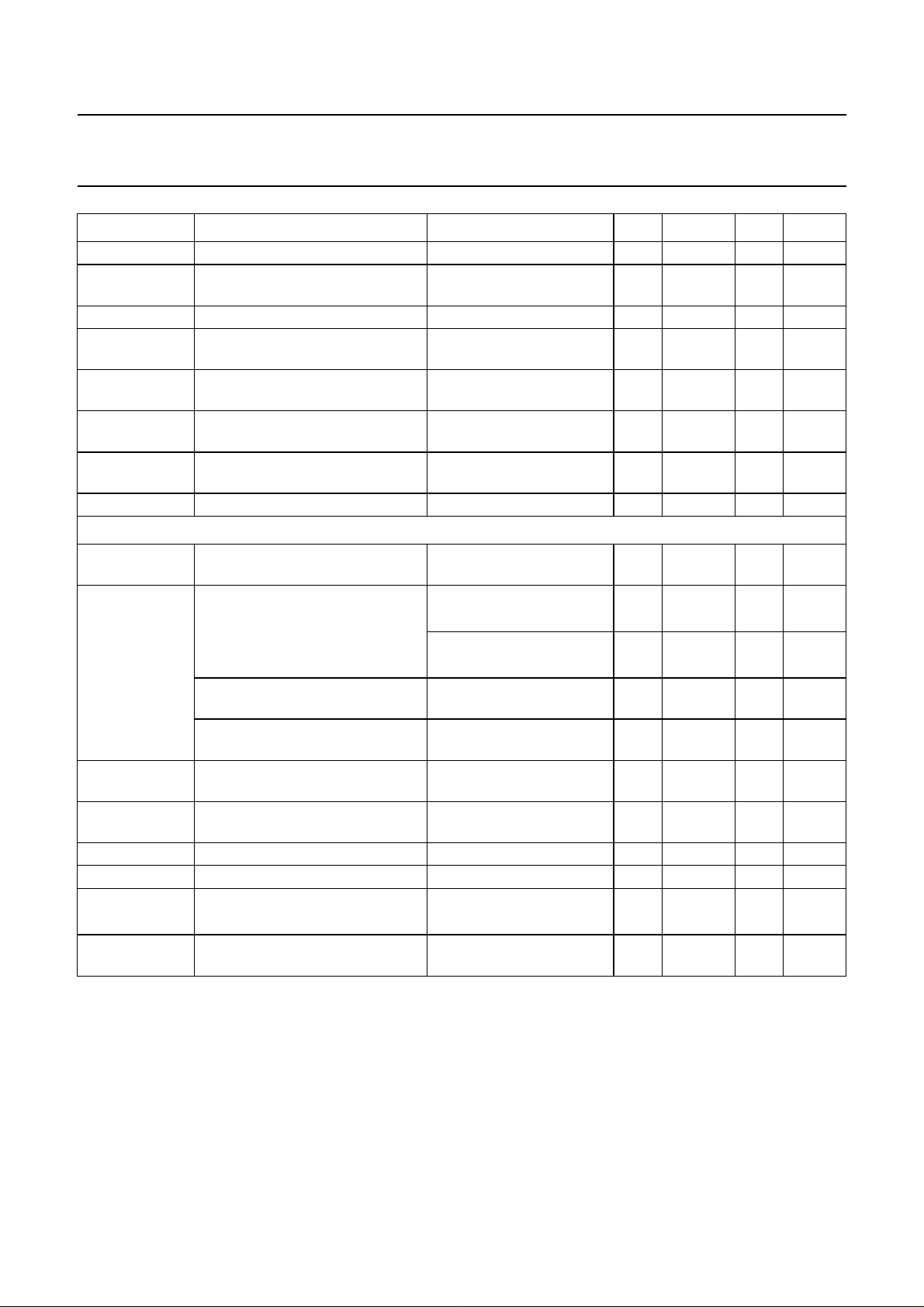
LIMITING VALUES
In accordance with the Absolute Maximum Rating System (IEC 134).
SYMBOL PARAMETER CONDITIONS MIN. MAX. UNIT
V
DDA1
V
DDA2
V
DDA3
V
DDD
T
stg
T
amb
V
es
Note
1. Charge device model class B: equivalent to discharging a 200 pF capacitor via a 0 Ω series resistor.
analog supply voltage 1 (pin 5) −0.3 +6.5 V
analog supply voltage 2 (pin 28) −0.3 +12 V
analog supply voltage 3 (pin 56) −0.3 +12 V
digital supply voltage (pin 52) −0.3 +6.5 V
storage temperature −55 +150 °C
operating ambient temperature −40 +85 °C
electrostatic handling note 1
pins 8 and 9 −100 +100 V
all other pins −300 +300 V
CHARACTERISTICS
V
DDA3=VDDA2
∆f = 22.5 kHz; R
= 8.5 V (ref. AGND); V
=50Ω; V
g
= 10 mV; with de-emphasis = 50 µs; unless otherwise specified.
37-35
= 5 V (ref. AGND); V
DDA1
= 5 V (ref. DGND); T
DDD
amb
=25°C; f
mod
= 1 kHz;
SYMBOL PARAMETER CONDITIONS MIN. TYP. MAX. UNIT
Current consumption
I
DDA1
analog supply current 1 (pin 5) FM mode 17 21 25 mA
AM mode 14 17 21 mA
I
DDA2
I
DDA3
analog supply current 2 (pin 28) FM mode 2.4 3.0 3.6 mA
analog supply current 3 (pin 56) FM mode 19 25 31 mA
AM mode 9.5 12 15 mA
I
DDD
I
19+I20
digital supply current (pin 52) 8 10 12 mA
total FM mixer output current
4.8 6.0 7.2 mA
pins 19 and 20
I
22+I23
total AM mixer output current
AM mode 10 12 14 mA
pins 22 and 23
FM-IF path; see Fig.3
V
19-20max(p-p)
maximum output voltage
12 14 − V
pins 19 to 20 (peak-to-peak value)
I
bias(19-20)
I
LI(19-20)
mixer bias current pins 19 to 20 2.4 3.0 3.6 mA
mixer leakage current
in AM position −− 2µA
pins 19 to 20
I
19IF2/V13-14IF1
R
i(13-14)
conversion gain 1.65 1.9 2.2 mS
input resistance between
57 −kΩ
pins 13 and 14
C
i(13-14)
input capacitance between
− 3 4.5 pF
pins 13 and 14
R
opt
optimum generator resistance − 1.2 − kΩ
1997 May 05 7
Philips Semiconductors Preliminary specification
In Car Entertainment (ICE) car radio TEA6824T
SYMBOL PARAMETER CONDITIONS MIN. TYP. MAX. UNIT
R
o(19-20)
C
; C
o(19-4)
o(20-4)
IP3 third-order intermodulation 114 124 − dBµV
Oscillator
f
osc
∆f
osc
∆f
/∆T temperature dependence of
osc
R
1
C
0
FM-IF
amplifier
2
V
27-24max(rms)
V
29-4max(rms)
V
29-4/V27-24
∆V
29-4/V27-24
R
i(27-4)
C
i(27-4)
R
o(29-4)
C
o(29-4)
output resistance between
15 20 − kΩ
pins 19 and 20
output capacitance between
− 12 14 pF
pins 19 to 4 and pins 20 to 4
oscillator frequency − 61.5 − MHz
oscillator frequency spread −− 250 Hz
−1
oscillator frequency
crystal type Philips
9922 521 00098
− 30 × 10−6− K
crystal motional resistance −− 70 Ω
crystal shunt capacitance −− 5pF
maximum input voltage for 1 dB
80 110 − mV
compression point between
pins 27 and 24 (RMS value)
maximum output voltage between
220 320 − mV
pins 29 and 4 (RMS value)
amplifier gain between
pins 29 and 4 and between
loaded with 330 Ω;
see Fig.4
912 15dB
pins 27 and 24
gain temperature dependence
− 0.05 − dB/K
between pins 29 and 4 and
between pins 27 and 24
input resistance between
300 330 360 Ω
pins 27 and 4
input capacitance between
−− 5pF
pins 27 and 4
output resistance between
300 330 360 Ω
pins 29 and 4
output capacitance between
−− 5pF
pins 29 and 4
FM-IF
limiter
2
V
o1-2(p-p)
limiter output voltage between
pins 1 and 2 (peak-to-peak value)
V
1-2/V37-35
limiter gain between pins 1 and 2
see Fig.5 − 80 − dB
and between pins 37 and 35
C
i(37-4)
input capacitance between
pins 37 and 4
R
o(1-2)
output resistance between
pins 1 and 2
C
o(1-2)
output capacitance between
pins 1 and 2
1997 May 05 8
500 700 − mV
−− 5pF
−− 1.0 kΩ
10 15 20 pF

Philips Semiconductors Preliminary specification
In Car Entertainment (ICE) car radio TEA6824T
SYMBOL PARAMETER CONDITIONS MIN. TYP. MAX. UNIT
FM demodulator
V
43-4(rms)
MPX output voltage between
pins 43 and 4 (RMS value)
V
37-35(rms)
start of limiting voltage between
αAF= −3dB − 25 40 µV
pins 37 and 35 (RMS value)
V
37-35(rms)
∆V
43DC
V
43FM/V43AM
input voltage for signal plus
noise-to-noise ratio (RMS value)
residual DC-offset voltage pin 43 ∆L
AM suppression pin 43 ∆f = 22.5 kHz;
see Fig.6;
SN+
-------------N
SN+
--------------
N
demod
10 µV<V
80 µV<V
f
= 1 kHz;
modAM
26 dB=
46dB=
= typical value;
37-35
37-35
mAM= 30%;
V
= 3 to 300 mV
37-35
∆V
43-44AFCdis
/∆V
43-44AFCactive
demodulator frequency control
voltage (AFC) efficiency between
pins 43 and 44 at 100 kHz detune
from exact tuning
R
o43
B
43
SN+
-------------N
output resistance pin 43 −− 1.5 kΩ
AF bandwidth pin 43 200 −−kHz
signal plus noise-to-noise ratio 66 75 − dB
THD total harmonic distortion at pin 43 detuning ≤50 kHz;
∆f = 75 kHz; f
mod
without de-emphasis;
L
= typical value;
demod
V
= 300 µV to 800 mV
37-35
<80µV − 100 1000 mV
< 800 mV − 10 30 mV
= 1 kHz
160 200 240 mV
− 30 45 µV
− 70 100 µV
50 60 − dB
28 32 − dB
− 0.1 0.35 %
1997 May 05 9
Philips Semiconductors Preliminary specification
In Car Entertainment (ICE) car radio TEA6824T
SYMBOL PARAMETER CONDITIONS MIN. TYP. MAX. UNIT
Unweighted voltage level
V
50-4
∆V
/∆V
50-4
37-35
∆V
/(V
50-4
50-4
I
source(max)
I
sink(max)
R
o50
ADJUSTMENT OF UNWEIGHTED VOLTAGE LEVEL AND V
∆V
50
V
38-4
∆V
/∆V
50-4
38-4
R
i38
Multi-path detector
f
MP
B
MP
Reference voltage
V
o(21-4)
∆V
/(V
21-4
21-4
I
o21
AM-IF path; see Fig.9 and notes 2 and 3
V
22-23max(p-p)
unweighted voltage level see Fig.7; V38= 2.52 V;
V
≤ 2.5 µV 1.6 2.2 3.0 V
37-35
V
= 1.0 mV 2.7 3.4 4.7 V
37-35
slope of unweighted voltage level 100 µV ≤ V
37-35(rms)
< 300 mV;
temperature
0.75 0.9 1.05 V/20 dB
compensation off
temperature
0.6 0.75 0.9 V/20 dB
compensation on
∆T) temperature dependence V
= 1 mV;
37-35
temperature
− 5.0 − mV/VK
compensation off
temperature
− 2.0 − mV/VK
compensation on
maximum output source current
0.3 −−mA
pin 50
maximum output sink current
−50 −−µA
pin 50
output resistance pin 50 −− 300 Ω
; note 1
mutaml
adjusting range voltage pin 50 V
37-35(rms)
=10mV −1.8 − +1.8 V
internal bias voltage − 2.6 − V
adjusting gain −−0.9 −
input resistance pin 38 − 80 − kΩ
multi-path detector band-pass
− 20 − kHz
centre frequency
band-pass bandwidth 7 −−kHz
output voltage I21= −1 mA 4.5 5.1 5.7 V
∆T) temperature dependence − 3.3 − mV/VK
output current pin 21 −− 1mA
maximum output voltage between
12 15 − V
pins 22 and 23
(peak-to-peak value)
1997 May 05 10
Philips Semiconductors Preliminary specification
In Car Entertainment (ICE) car radio TEA6824T
SYMBOL PARAMETER CONDITIONS MIN. TYP. MAX. UNIT
I
bias(22-23)
I
LI(22-23)
I
22IF2/V27-24IF1
R
i(27-24)
C
i(27-24)
R
o(22-23)
C
o(22-23)
IP3 third order intermodulation − 137 − dBµV
AM
DETECTOR; see notes 4 and 5
V
48-4(rms)
V
33-34(rms)
R
i(33-34)
C
i(33-34)
R
o48
C
o48
SN+
-------------N
THD total harmonic distortion m = 0.8;
Notes to the Characteristics
1. For typical adjusting range see Fig.8.
2. f
= 10.7 MHz; f
IF1
3. The AM oscillator signal is generated by division of the 61.5 MHz crystal oscillator. Two divider ratios programmable
by the I2C-bus: division by 6 (AM-IF1= 10.7 MHz); division by 2 (AM-IF1= 30 MHz).
4. For typical AM level curve see Fig.10.
5. For AM detector; f
mixer bias current pins 22 and 23 5 6 7 mA
mixer leakage current
in FM position −− 2µA
pins 22 and 23
conversion gain 2.2 2.7 3.4 mS
input resistance between
300 330 360 Ω
pins 27 and 24
input capacitance between
− 58pF
pins 27 and 24
output resistance between
10 20 − kΩ
pins 22 and 23
output capacitance between
− 510pF
pins 22 and 23
AF output level (RMS value) R
sensitivity voltage (RMS value) − 50 75 µV
minimum input voltage
AM-IF
2
> 500 kΩ;
L48
100 µV ≤ V
SN+
-------------N
SN+
-------------N
26 dB=
46dB=
33-34
≤ 300 mV
190 240 290 mV
− 200 400 µV
THD ≤ 5%; m = 0.8 −− 100 µV
(RMS value)
AM-IF
maximum input voltage
2
THD ≤ 5%; m = 0.8 800 −−mV
(RMS value)
IF2 input resistance between
1.8 2.0 2.2 kΩ
pins 33 and 34
IF2 input capacitance between
− 10 15 pF
pins 33 and 34
output resistance pin 48 27 33 39 kΩ
output capacitance pin 48 −− 10 pF
signal-plus-noise-to-noise ratio 54 60 − dB
− 1.5 3.0 %
450 kHz for AM mixer.
IF2 =
= 450 kHz; f
AMIF2
= 400 Hz; m = 30%.
mod
300 µV ≤ V
33-34
≤ 200 mV
1997 May 05 11
 Loading...