

Page 1

INTEGRATED CIRCUITS
DATA SH EET
TEA5767HL
Low-power FM stereo radio for
handheld applications
Product specification
Supersedes data of 2003 Nov 06
2004 Sep 13
Page 2

Philips Semiconductors Product specification
Low-power FM stereo radio for
handheld applications
CONTENTS
1 FEATURES
2 GENERAL DESCRIPTION
3 ORDERING INFORMATION
4 QUICK REFERENCE DATA
5 BLOCK DIAGRAM
6 PINNING
7 FUNCTIONAL DESCRIPTION
7.1 Low-noise RF amplifier
7.2 FM mixer
7.3 VCO
7.4 Crystal oscillator
7.5 PLL tuning system
7.6 RF AGC
7.7 IF filter
7.8 FM demodulator
7.9 Level voltage generator and analog-to-digital
converter
7.10 IF counter
7.11 Soft mute
7.12 MPX decoder
7.13 Signal dependent mono to stereo blend
7.14 Signal dependent AF response
7.15 Software programmable ports
8 3-WIRE BUS AND BUS-CONTROLLED
FUNCTIONS
8.1 3-wire bus specification
8.1.1 Data transfer
8.1.2 Power-on reset
8.2 Writing data
8.3 Reading data
8.4 Bus timing
TEA5767HL
9 LIMITING VALUES
10 THERMAL CHARACTERISTICS
11 DC CHARACTERISTICS
12 AC CHARACTERISTICS
13 INTERNAL PIN CONFIGURATION
14 APPLICATION INFORMATION
15 PACKAGE OUTLINE
16 SOLDERING
16.1 Introduction to soldering surface mount
packages
16.2 Reflow soldering
16.3 Wave soldering
16.4 Manual soldering
16.5 Suitability of surface mount IC packages for
wave and reflow soldering methods
17 DATA SHEET STATUS
18 DEFINITIONS
19 DISCLAIMERS
2004 Sep 13 2
Page 3

Philips Semiconductors Product specification
Low-power FM stereo radio for
handheld applications
1 FEATURES
• High sensitivity due to integrated low-noise RF input
amplifier
• FM mixer for conversion to IF of the US/Europe
(87.5 MHz to 108 MHz) and Japanese
(76 MHz to 91 MHz) FM band
• Preset tuning to receive Japanese TV audio up to
108 MHz
• RF Automatic Gain Control (AGC) circuit
• LC tuner oscillator operating with low cost fixed chip
inductors
• FM IF selectivity performed internally
• No externaldiscriminatorneeded due to fully integrated
FM demodulator
• Crystal reference frequency oscillator; the oscillator
operates with a 32.768 kHz clock crystal or with a
13 MHz crystal and with an externally applied 6.5 MHz
reference frequency
• PLL synthesizer tuning system
• 3-wire bus
• 7-bit IF counter output via the 3-wire bus
• 4-bit level information output via the 3-wire bus
TEA5767HL
• Soft mute
• Signal dependent mono to stereo blend [Stereo Noise
Cancelling (SNC)]
• Signal dependent High Cut Control (HCC)
• Soft mute, SNC and HCC can be switched off via the
3-wire bus
• Adjustment-free stereo decoder
• Autonomous search tuning function
• Standby mode
• Two software programmable ports
• Bus enable line to switch the bus input and output lines
into 3-state mode.
2 GENERAL DESCRIPTION
The TEA5767HL is a single-chip electronically tuned FM
stereo radio for low-voltage applications with fully
integrated IF selectivity and demodulation. The radio is
completely adjustment-free and only requires a minimum
of small and low cost external components. The radio can
be tuned to the European, US and Japanese FM bands.
3 ORDERING INFORMATION
TYPE
NUMBER
TEA5767HL LQFP32 plastic low profile quad flat package; 32 leads; body 7 × 7 × 1.4 mm SOT358-1
NAME DESCRIPTION VERSION
PACKAGE
2004 Sep 13 3
Page 4
Philips Semiconductors Product specification
Low-power FM stereo radio for
TEA5767HL
handheld applications
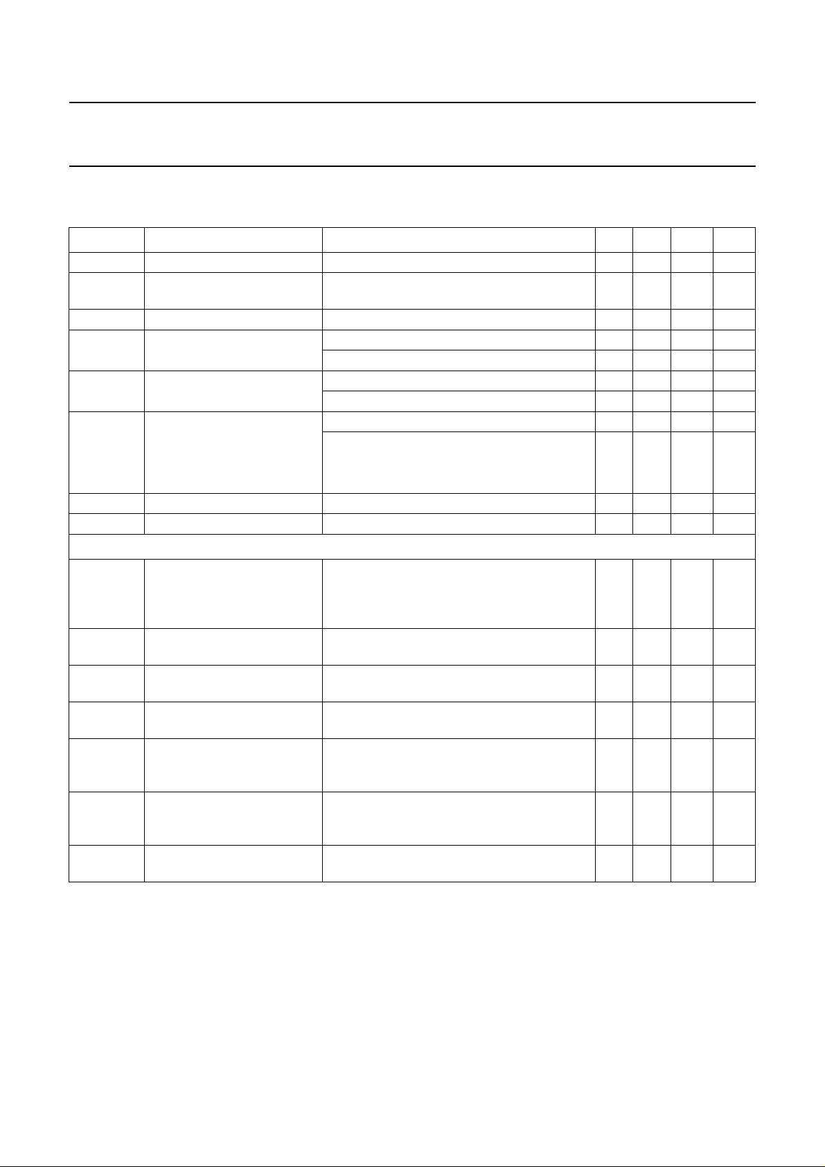
4 QUICK REFERENCE DATA
V
CCA=VCC(VCO)=VCCD
SYMBOL PARAMETER CONDITIONS MIN. TYP. MAX. UNIT
V
CCA
V
CC(VCO)
analog supply voltage 2.5 3.0 5.0 V
voltage controlled oscillator
supply voltage
V
CCD
I
CCA
I
CC(VCO)
digital supply voltage 2.5 3.0 5.0 V
analog supply current operating; V
voltage controlled oscillator
supply current
I
CCD
f
FM(ant)
T
amb
digital supply current operating; V
FM input frequency 76 − 108 MHz
ambient temperature V
FM overall system parameters; see Fig.7
V
S
S
RF
−200
+200
RF sensitivity input voltage fRF= 76 MHz to 108 MHz; ∆f = 22.5 kHz;
LOW side 200 kHz selectivity ∆f=−200 kHz; fRF= 76 MHz to 108 MHz;
HIGH side 200 kHz
selectivity
V
AFL
; V
left and right audio frequency
AFR
output voltage
(S+N)/N maximum signal plus
noise-to-noise ratio
α
cs(stereo)
stereo channel separation VRF= 1 mV; R = L = 0 or R = 0 and L = 1
THD total harmonic distortion VRF= 1 mV;L = R; ∆f = 75 kHz;f
.
2.5 3.0 5.0 V
= 3 V 6.0 8.4 10.5 mA
CCA
standby mode; V
operating; V
VCOTANK1=VVCOTANK2
standby mode; V
CCD
standby mode; V
=3V − 36 µA
CCA
= 3 V 560 750 940 µA
VCOTANK1=VVCOTANK2
=3V − 12 µA
= 3 V 2.1 3.0 3.9 mA
=3V
CCD
bus enable line HIGH 30 56 80 µA
bus enable line LOW 11 19 26 µA
CCA=VCC(VCO)=VCCD
=2.5Vto5V −10 − +75 °C
− 2 3.5 µV
f
= 1 kHz; (S+N)/N = 26 dB;
mod
de-emphasis = 75 µs; L = R;
BAF= 300 Hz to 15 kHz
32 36 − dB
note 1
∆f = +200 kHz; fRF= 76 MHz to 108 MHz;
39 43 − dB
note 1
VRF= 1 mV; L = R; ∆f = 22.5 kHz;
f
= 1 kHz; de-emphasis = 75 µs
mod
VRF= 1 mV; L = R; ∆f = 22.5 kHz;
f
= 1 kHz; de-emphasis = 75 µs;
mod
60 75 90 mV
54 60 − dB
BAF= 300 Hz to 15 kHz
24 30 − dB
including 9 %pilot; ∆f = 75 kHz; f
mod
= 1 kHz;
data byte 3 bit 3 = 0; data byte 4 bit1=1
mod
= 1 kHz;
− 0.4 1 %
de-emphasis = 75 µs
Note
1. LOWside andHIGH side selectivitycan be switchedby changing themixer from HIGHside to LOWside LOinjection.
2004 Sep 13 4
Page 5
This text is here in white to force landscape pages to be rotated correctly when browsing through the pdf in the Acrobat reader.This text is here in
_white to force landscape pages to be rotated correctly when browsing through the pdf in the Acrobat reader.This text is here inThis text is here in
white to force landscape pages to be rotated correctly when browsing through the pdf in the Acrobat reader. white to force landscape pages to be ...
2004 Sep 13 5
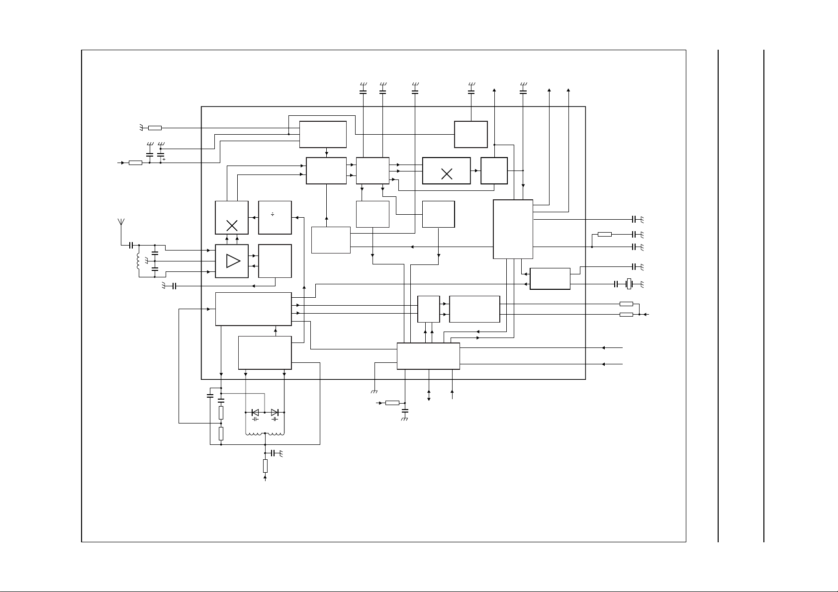
5 BLOCK DIAGRAM
Philips Semiconductors Product specification
Low-power FM stereo radio for
handheld applications
V
CCA
FM antenna
22 nF
4.7 Ω
100 pF
L1
47 nF 47 nF 33 nF
LIMDEC2
24 23 22 21 20
R1
27 pF
47 pF
22 µF
4.7 nF
LOOPSW
I
gain
AGND
V
CCA
RFI1
RFGND
RFI2
TAGC
25
26
27
I/Q-MIXER
1st FM
28
29
30
31
32
TUNING SYSTEM
12
CPOUT VCOTANK2 V
39 nF10 nF
10 kΩ
100 kΩ
AGC
VCO
VCOTANK1
D1 D2
L3
2
N1
L2
GAIN
STABILIZATION
RESONANCE
AMPLIFIER
IF CENTRE
FREQUENCY
ADJUST
programmable divider output
reference frequency divider output
34
CC(VCO)
LIMDEC1 TIFC V
LIMITER
LEVEL
ADC
5678
DGND CLOCK
12 Ω
V
CCD
47 nF
DEMODULATOR
COUNTER
I
ref
MUX
3-WIRE BUS
CCD
22 nF
IF
TEA5767HL
PROGRAMMABLE
DATAV
ref
POWER
SUPPLY
SOFTWARE
PORT
pilot
mono
MPXO TMUTE
SOFT
MUTE
MPX
DECODER
33 nF
V
AFR
19 18 17
SDS
CRYSTAL
OSCILLATOR
mhc245
V
AFL
16
15
14
13
12
11
10
9
PILFIL
33 kΩ
PHASEFIL
XTAL2
C
pull
XTAL1
SWPORT2
SWPORT1
BUSENABLE
WRITE/READ
1 nF
22 nF
22 nF
(1)
10 kΩ
10 kΩ
C
comp
(1)
32.768 kHz
or
13 MHz
V
CCA
The component list is given in Chapter 14.
(1) C
comp
and C
data depends on crystal specification.
pull
47 Ω
22 nF
V
CC(VCO)
TEA5767HL
Fig.1 Block diagram.
Page 6

Philips Semiconductors Product specification
Low-power FM stereo radio for
handheld applications
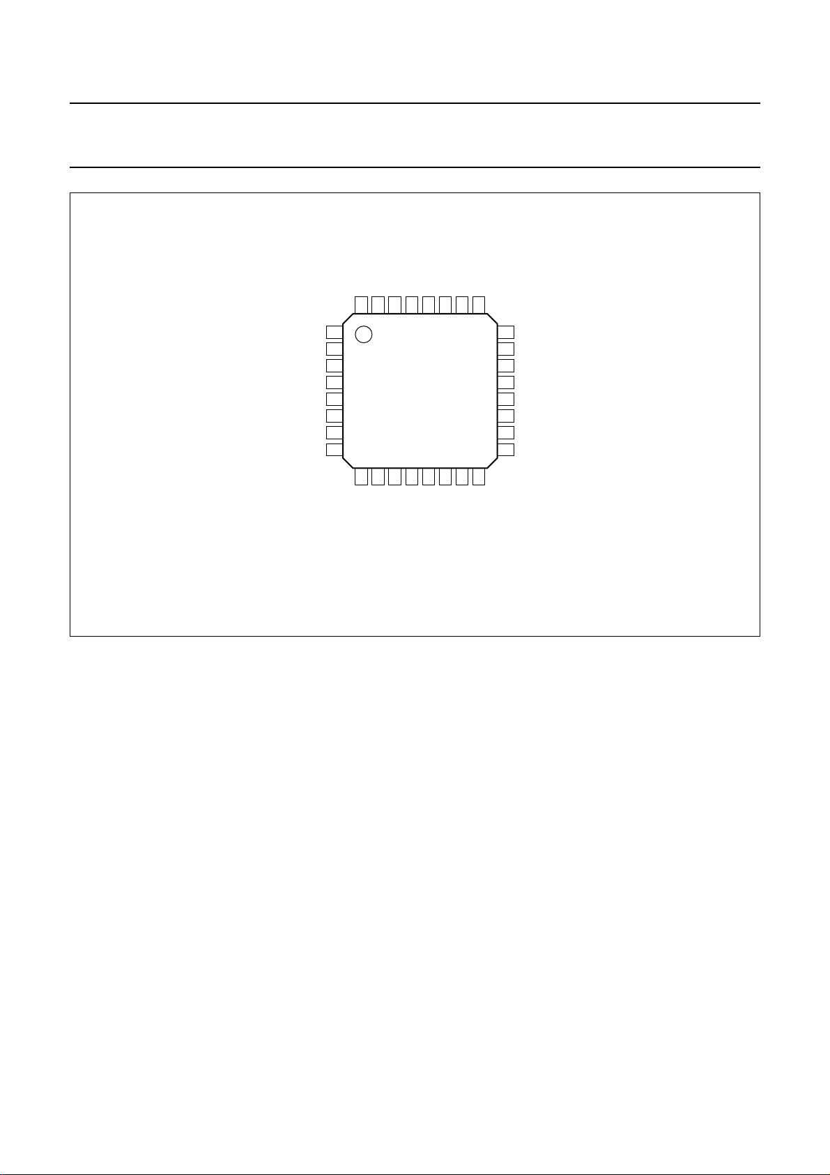
6 PINNING
SYMBOL PIN DESCRIPTION
CPOUT 1 charge pump output of synthesizer PLL
VCOTANK1 2 voltage controlled oscillator tuned circuit output 1
VCOTANK2 3 voltage controlled oscillator tuned circuit output 2
V
CC(VCO)
DGND 5 digital ground
V
CCD
DATA 7 bus data line input/output
CLOCK 8 bus clock line input
WRITE/READ 9 write/read control input for the 3-wire bus
BUSENABLE 10 bus enable input
SWPORT1 11 software programmable port 1
SWPORT2 12 software programmable port 2
XTAL1 13 crystal oscillator input 1
XTAL2 14 crystal oscillator input 2
PHASEFIL 15 phase detector loop filter
PILFIL 16 pilot detector low-pass filter
V
AFL
V
AFR
TMUTE 19 time constant for soft mute
MPXO 20 FM demodulator MPX signal output
V
ref
TIFC 22 time constant for IF centre adjust
LIMDEC1 23 decoupling IF limiter 1
LIMDEC2 24 decoupling IF limiter 2
I
gain
AGND 26 analog ground
V
CCA
RFI1 28 RF input 1
RFGND 29 RF ground
RFI2 30 RF input 2
TAGC 31 time constant RF AGC
LOOPSW 32 switch output of synthesizer PLL loop filter
4 voltage controlled oscillator supply voltage
6 digital supply voltage
17 left audio frequency output voltage
18 right audio frequency output voltage
21 reference voltage
25 gain control current for IF filter
27 analog supply voltage
TEA5767HL
2004 Sep 13 6
Page 7
Philips Semiconductors Product specification
Low-power FM stereo radio for
handheld applications
CPOUT LIMDEC2
VCOTANK1 LIMDEC1
VCOTANK2 TIFC
V
CC(VCO)
CLOCK V
1
2
3
4
5
DGND MPXO
6
V
CCD
7
DATA V
8
CCA
32313029282726
TEA5767HL
9
10111213141516
XTAL1 RFI1
XTAL2 V
SWPORT1 RFI2
SWPORT2 RFGND
BUSENABLE TAGC
WRITE/READ LOOPSW
25
PILFIL I
PHASEFIL AGND
gain
24
23
22
21
V
ref
20
19
TMUTE
18
AFR
17
AFL
001aab573
TEA5767HL
Fig.2 Pin configuration.
7 FUNCTIONAL DESCRIPTION
7.1 Low-noise RF amplifier
The LNA input impedance together with the LC RF input
circuit defines an FM band filter. The gain of the LNA is
controlled by the RF AGC circuit.
7.2 FM mixer
The FM quadrature mixer converts the FM RF
(76 MHz to 108 MHz) to an IF of 225 kHz.
7.3 VCO
The varactor tuned LC VCO provides the Local Oscillator
(LO) signal for the FM quadrature mixer. The VCO
frequency range is 150 MHz to 217 MHz.
7.4 Crystal oscillator
The crystal oscillator can operate with a 32.768 kHz clock
crystal or a 13 MHz crystal. The temperature drift of
standard 32.768 kHz clock crystals limits the operational
temperature range from −10 °C to +60 °C.
The PLL synthesizer can be clocked externally with a
32.768 kHz, a 6.5 MHz or a 13 MHz signal via pin XTAL2.
The crystal oscillator generates the reference frequency
for:
• The reference frequency divider for the synthesizer PLL
• The timing for the IF counter
• The free-running frequency adjustment of the stereo
decoder VCO
• The centre frequency adjustment of the IF filters.
7.5 PLL tuning system
The PLL synthesizer tuning system is suitable to operate
with a 32.768 kHz or a 13 MHz reference frequency
generated by thecrystal oscillatoror applied to the ICfrom
an external source. The synthesizer can also be clocked
via pin XTAL2 at 6.5 MHz. The PLL tuning system can
perform an autonomous search tuning function.
7.6 RF AGC
The RF AGC prevents overloading and limits the amount
of intermodulation products created by strong adjacent
channels.
2004 Sep 13 7
Page 8

Philips Semiconductors Product specification
Low-power FM stereo radio for
handheld applications
7.7 IF filter
Fully integrated IF filter.
7.8 FM demodulator
The FM quadrature demodulator has an integrated
resonator to perform the phase shift of the IF signal.
7.9 Level voltage generator and analog-to-digital converter
TheFM IF analoglevel voltage isconvertedto 4 bits digital
data and output via the 3-wire bus.
7.10 IF counter
The IF counter outputs a 7-bit count result via the 3-wire
bus.
7.11 Soft mute
The low-pass filtered level voltage drives the soft mute
attenuator at low RF input levels. The soft mute function
can be switched off via the 3-wire bus.
7.12 MPX decoder
The PLL stereo decoder is adjustment-free. The stereo
decoder can be switched to mono via the 3-wire bus.
7.13 Signal dependent mono to stereo blend
With a decreasing RF input level the MPX decoder blends
from stereo to mono to limit the output noise. The
continuousmono tostereo blend canalso be programmed
viathe3-wire bus toanRFlevel depending switched mono
tostereo transition.Stereo Noise Cancelling(SNC) can be
switched off via the 3-wire bus.
7.14 Signal dependent AF response
Theaudio bandwidthwill be reducedwith a decreasingRF
input level. This function can be switched off via the3-wire
bus.
7.15 Software programmable ports
Two software programmableports (open-collector) canbe
addressed via the 3-wire bus.
The port 1 (pin SWPORT1) function can be changed with
write data byte 4 bit 0 (see Table 10). Pin SWPORT1 is
then output for the ready flag of read byte 1.
TEA5767HL
8 3-WIRE BUS AND BUS-CONTROLLED
FUNCTIONS
8.1 3-wire bus specification
The3-wire bus controls thewrite/read,clock and data lines
and operates at a maximum clock frequency of 400 kHz.
Before any READ or WRITE operation the pin
BUSENABLE has to be HIGH for at least 10 µs.
Hint: By using the standby bit the IC can be switched into
a low current standby mode. In standby mode the IC must
be in the WRITE mode. When the IC is switched to READ
mode, during standby, the IC will hold the data line down.
The standby current can be reduced by deactivating the
bus interface (pin BUSENABLE LOW). If thebus interface
is deactivated (pin BUSENABLE LOW) without the
standby mode being programmed, the IC maintains
normal operation, but is isolated from the clock and data
line.
8.1.1 DATA TRANSFER
Data sequence: byte 1, byte 2, byte 3, byte 4 and byte 5
(the data transfer has to be in this order).
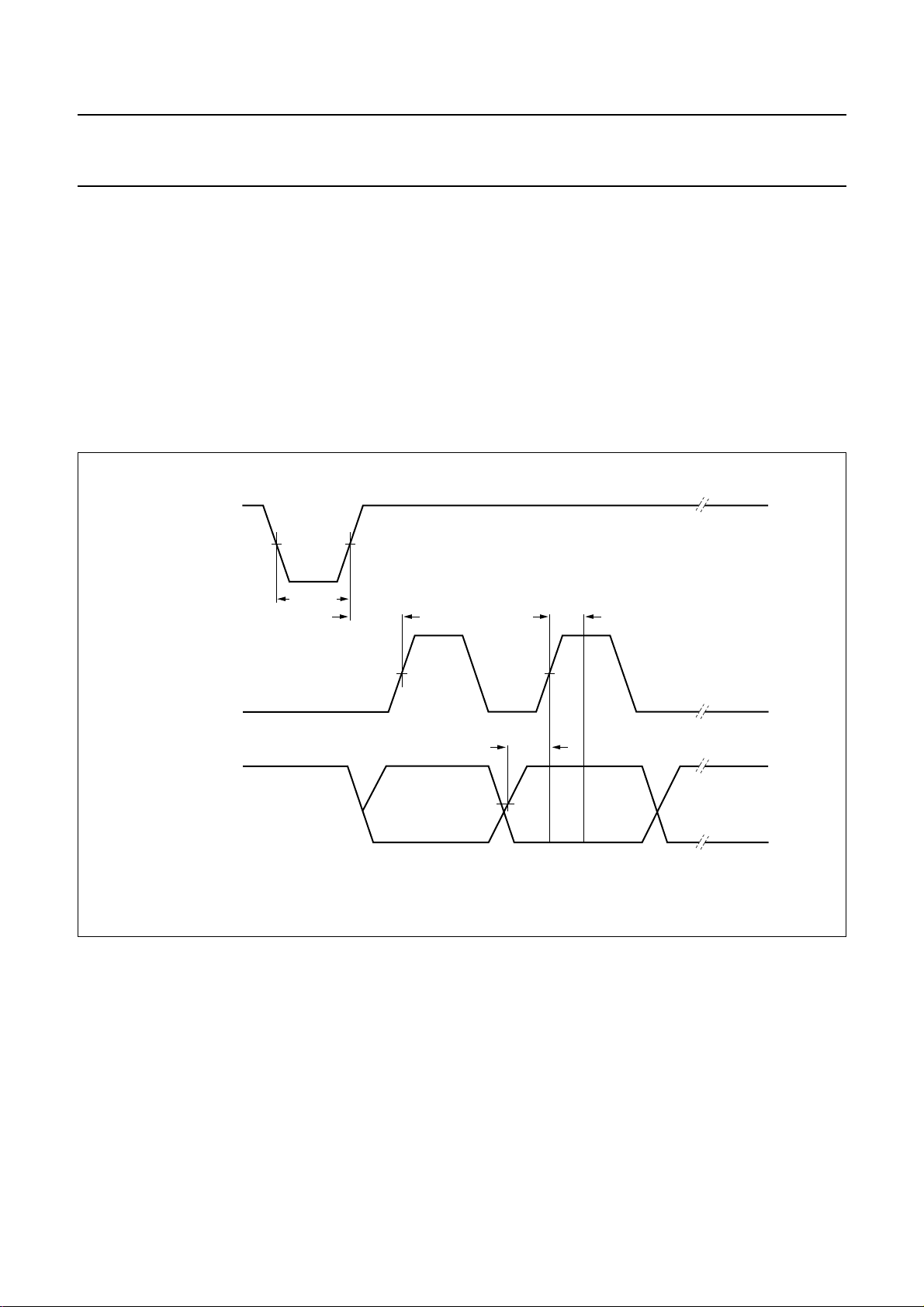
A positive edge at pin WRITE/READ enables the data
transfer into the IC. The data has to be stable at the
positive edge of the clock. Data may change while the
clock is LOWand is writteninto theIC on thepositive edge
of the clock. Data transfer can be stopped after the
transmission of new tuning information with the first two
bytes or after each following byte.
A negative edge at pin WRITE/READ enables the data
transfer from the IC. The WRITE/READ pin changeswhile
the clock is LOW. With the negative edge at
pin WRITE/READ the MSB of the first byte occurs at
pin DATA.
The bits are shifted on the negative clock edge to pin
DATA and can be read on the positive edge.
To do two consecutive read or write actions,
pin WRITE/READ has to be toggled for at least one clock
period. When a search tuning request is sent, the IC
autonomously starts searching the FM band; the search
direction and search stop level can be selected. When a
station with a field-strength equal to or greater than the
stop level is found, the tuning system stops and the ready
flag bit is set to HIGH. When, during search, a band limit is
reached, the tuning system stops at the band limit and the
band limit flag bit is set to HIGH. The ready flag is also set
to HIGH in this case.
2004 Sep 13 8
Page 9
Philips Semiconductors Product specification
Low-power FM stereo radio for
handheld applications
The software programmable output (SWPORT1) can be
programmed to operate as a tuning indicator output.
As long as the IC has not completed a tuning action,
pin SWPORT1 remains LOW. The pin becomes HIGH,
when a preset or search tuning is completed or when a
band limit is reached.
The reference frequency divider of the synthesizer PLL is
changed when the MSB in byte 5 is set to logic 1. The
tuning system can then be clocked via pin XTAL2 at
6.5 MHz.
8.2 Writing data
50 %WRITE/READ
TEA5767HL
8.1.2 POWER-ON RESET
At Power-on reset the mute is set, all other bits are
random.To initializethe IC allbytes have tobe transferred.
CLOCK
DATA
t
W(write)
t
su(clk)
50 % 50 %
t
su(write)
50 %
Fig.3 3-wire bus write data.
valid
data
t
h(write)
mhc250
2004 Sep 13 9
Page 10
Philips Semiconductors Product specification
Low-power FM stereo radio for
TEA5767HL
handheld applications
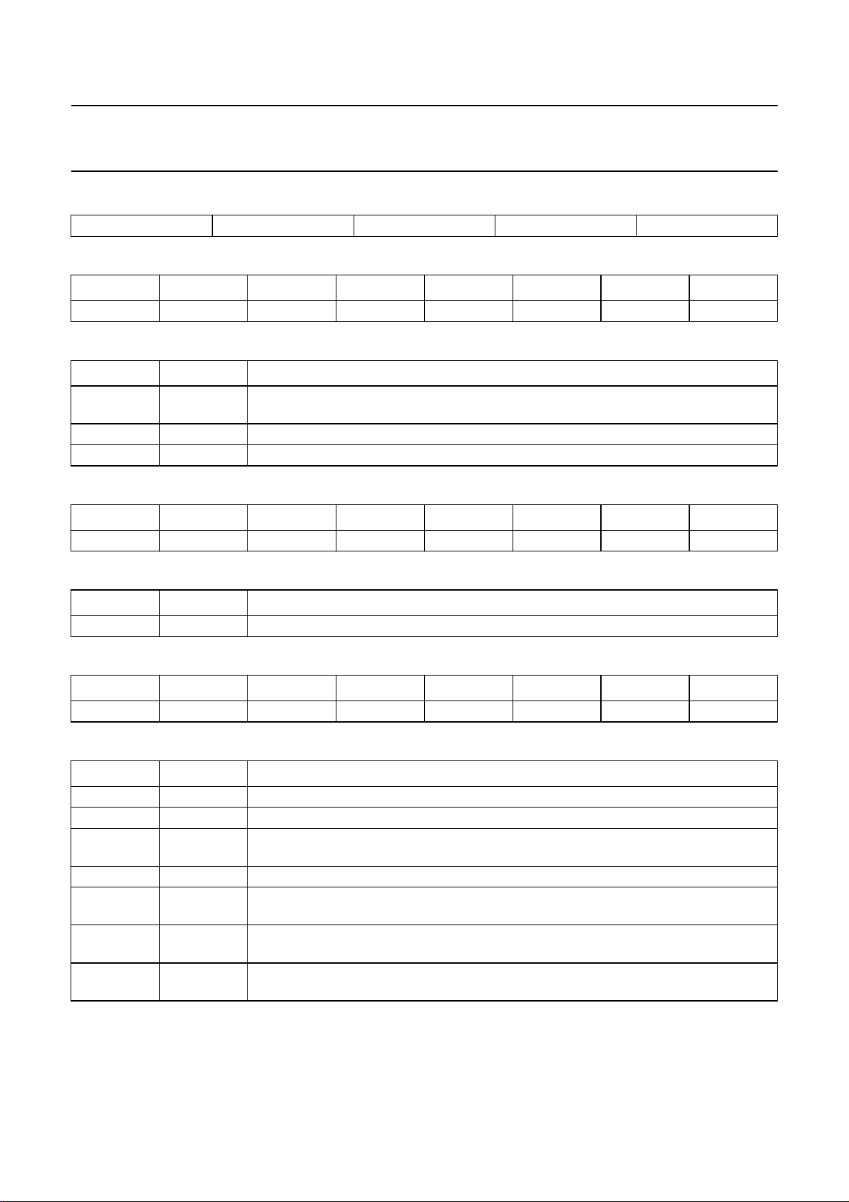
Table 1 Write mode
DATA BYTE 1 DATA BYTE 2 DATA BYTE 3 DATA BYTE 4 DATA BYTE 5
Table 2 Format of 1st data byte
BIT 7 (MSB) BIT 6 BIT 5 BIT 4 BIT 3 BIT 2 BIT 1 BIT 0 (LSB)
MUTE SM PLL13 PLL12 PLL11 PLL10 PLL9 PLL8
Table 3 Description of 1st data byte bits
BIT SYMBOL DESCRIPTION
7 MUTE if MUTE = 1 then L and R audio are muted; if MUTE = 0 then L and R audio are not
muted
6SMSearch Mode: if SM = 1 then in search mode; if SM = 0 then not in search mode
5 to 0 PLL[13:8] setting of synthesizer programmable counter for search or preset
Table 4 Format of 2nd data byte
BIT 7 (MSB) BIT 6 BIT 5 BIT 4 BIT 3 BIT 2 BIT 1 BIT 0 (LSB)
PLL7 PLL6 PLL5 PLL4 PLL3 PLL2 PLL1 PLL0
Table 5 Description of 2nd data byte bits
BIT SYMBOL DESCRIPTION
7 to 0 PLL[7:0] setting of synthesizer programmable counter for search or preset
Table 6 Format of 3rd data byte
BIT 7 (MSB) BIT 6 BIT 5 BIT 4 BIT 3 BIT 2 BIT 1 BIT 0 (LSB)
SUD SSL1 SSL0 HLSI MS MR ML SWP1
Table 7 Description of 3rd data byte bits
BIT SYMBOL DESCRIPTION
7 SUD Search Up/Down: if SUD = 1 then search up; if SUD = 0 then search down
6 and 5 SSL[1:0] Search Stop Level: see Table 8
4 HLSI HIGH/LOW Side Injection: if HLSI = 1 then HIGH side LO injection; if HLSI = 0 then
LOW side LO injection
3MSMono to Stereo: if MS = 1 then forced mono; if MS = 0 then stereo ON
2MRMute Right: if MR = 1 then the right audio channel is muted and forced mono; if MR = 0
then the right audio channel is not muted
1MLMute Left: if ML = 1 then the left audio channel is muted and forced mono; if ML = 0
then the left audio channel is not muted
0 SWP1 Software programmable port 1: if SWP1 = 1 then port 1 is HIGH; if SWP1 = 0 then
port 1 is LOW
2004 Sep 13 10
Page 11
Philips Semiconductors Product specification
Low-power FM stereo radio for
TEA5767HL
handheld applications
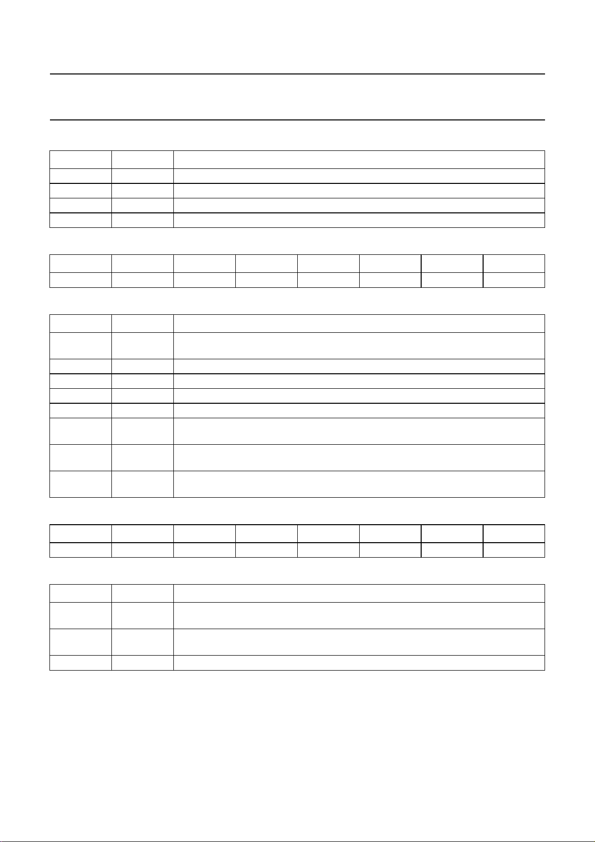
Table 8 Search stop level setting
SSL1 SSL0 SEARCH STOP LEVEL
0 0 not allowed in search mode
0 1 low; level ADC output= 5
1 0 mid; level ADC output = 7
1 1 high; level ADC output = 10
Table 9 Format of 4th data byte
BIT 7 (MSB) BIT 6 BIT 5 BIT 4 BIT 3 BIT 2 BIT 1 BIT 0 (LSB)
SWP2 STBY BL XTAL SMUTE HCC SNC SI
Table 10 Description of 4th data byte bits
BIT SYMBOL DESCRIPTION
7 SWP2 Software programmable port 2: if SWP2 = 1 then port 2 is HIGH; if SWP2 = 0 then
port 2 is LOW
6 STBY Standby: if STBY = 1 then in standby mode; if STBY = 0 then not in standby mode
5BLBand Limits: if BL = 1 then Japanese FM band; if BL = 0 then US/Europe FM band
4 XTAL if XTAL = 1 then f
3 SMUTE Soft MUTE: if SMUTE = 1 then soft mute is ON; if SMUTE = 0 then soft mute is OFF
2 HCC High Cut Control: if HCC = 1 then high cut control is ON; if HCC = 0 then high cut
control is OFF
1 SNC Stereo Noise Cancelling: if SNC = 1 then stereo noise cancelling is ON; if SNC = 0
then stereo noise cancelling is OFF
0SISearch Indicator: if SI = 1 then pin SWPORT1 is output forthe ready flag; if SI = 0 then
pin SWPORT1 is software programmable port 1
= 32.768 kHz; if XTAL = 0 then f
xtal
= 13 MHz
xtal
Table 11 Format of 5th data byte
BIT 7 (MSB) BIT 6 BIT 5 BIT 4 BIT 3 BIT 2 BIT 1 BIT 0 (LSB)
PLLREF DTC −−−−−−
Table 12 Description of 5th data byte bits
BIT SYMBOL DESCRIPTION
7 PLLREF if PLLREF = 1 then the 6.5 MHz reference frequency for the PLL is enabled;
if PLLREF = 0 then the 6.5 MHz reference frequency for the PLL is disabled
6 DTC if DTC = 1 then the de-emphasis time constant is 75 µs; if DTC = 0 then the
de-emphasis time constant is 50 µs
5to0 − not used; position is don’t care
2004 Sep 13 11
Page 12
Philips Semiconductors Product specification
Low-power FM stereo radio for
handheld applications
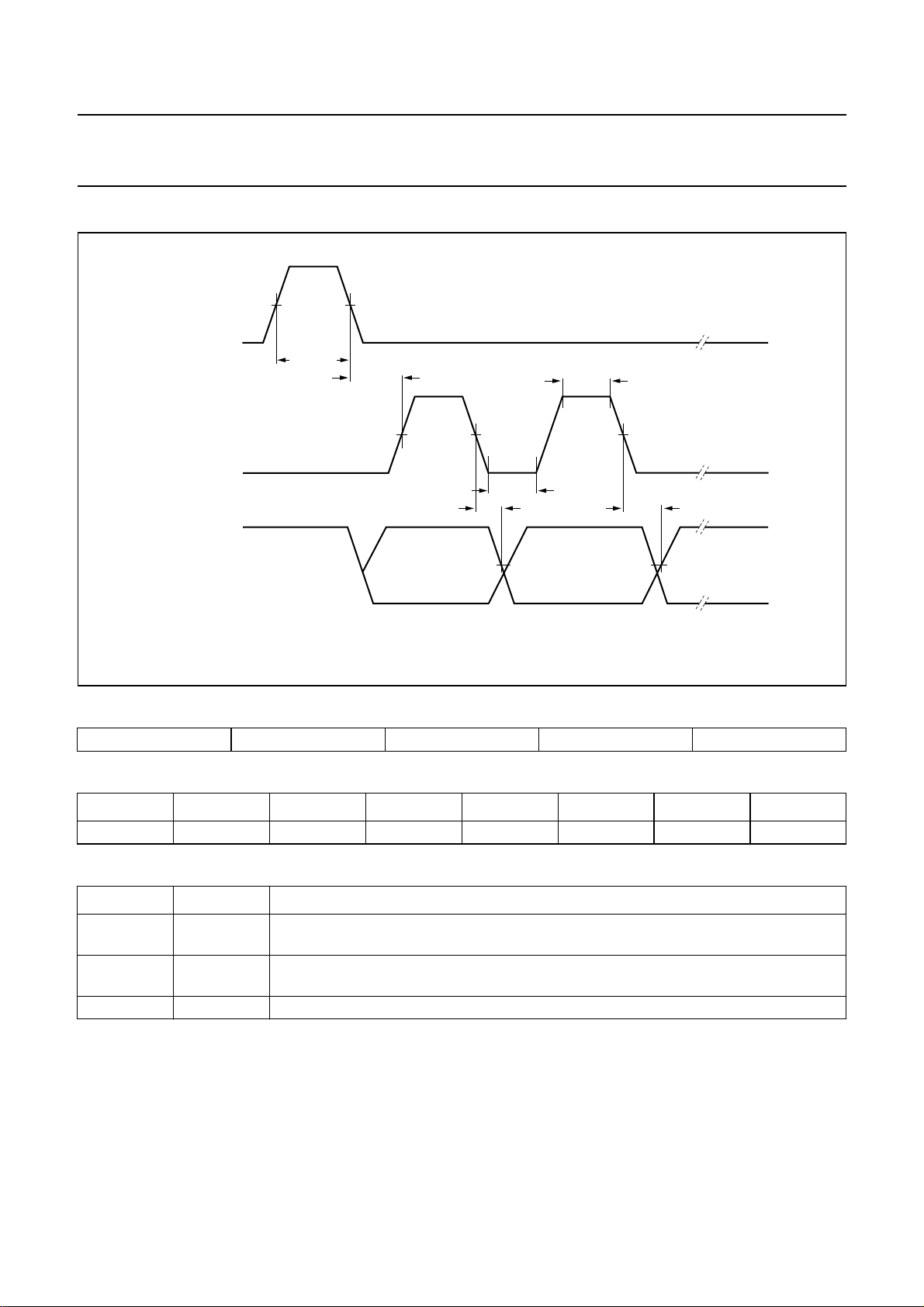
8.3 Reading data
t
W(read)
CLOCK
DATA
50 %WRITE/READ
t
su(clk)
50 %
50 %
t
LOW
t
h(out)
t
HIGH
50 %
t
d(out)
TEA5767HL
50 %
mhc249
Fig.4 3-wire bus read data.
Table 13 Read mode
DATA BYTE 1 DATA BYTE 2 DATA BYTE 3 DATA BYTE 4 DATA BYTE 5
Table 14 Format of 1st data byte
BIT 7 (MSB) BIT 6 BIT 5 BIT 4 BIT 3 BIT 2 BIT 1 BIT 0 (LSB)
RF BLF PLL13 PLL12 PLL11 PLL10 PLL9 PLL8
Table 15 Description of 1st data byte bits
BIT SYMBOL DESCRIPTION
7RFReady Flag: if RF = 1 then a station has been found or the band limit has been
reached; if RF = 0 then no station has been found
6 BLF Band Limit Flag: if BLF = 1 then the band limit has been reached; if BLF = 0 then the
band limit has not been reached
5 to 0 PLL[13:8] setting of synthesizer programmable counter after search or preset
2004 Sep 13 12
Page 13
Philips Semiconductors Product specification
Low-power FM stereo radio for
TEA5767HL
handheld applications
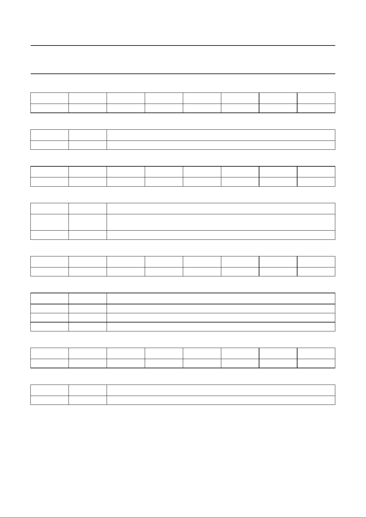
Table 16 Format of 2nd data byte
BIT 7 (MSB) BIT 6 BIT 5 BIT 4 BIT 3 BIT 2 BIT 1 BIT 0 (LSB)
PLL7 PLL6 PLL5 PLL4 PLL3 PLL2 PLL1 PLL0
Table 17 Description of 2nd data byte bits
BIT SYMBOL DESCRIPTION
7 to 0 PLL[7:0] setting of synthesizer programmable counter after search or preset
Table 18 Format of 3rd data byte
BIT 7 (MSB) BIT 6 BIT 5 BIT 4 BIT 3 BIT 2 BIT 1 BIT 0 (LSB)
STEREO IF6 IF5 IF4 IF3 IF2 IF1 IF0
Table 19 Description of 3rd data byte bits
BIT SYMBOL DESCRIPTION
7 STEREO Stereo indication: if STEREO = 1 then stereo reception; if STEREO = 0 then mono
reception
6 to 0 PLL[13:8] IF counter result
Table 20 Format of 4th data byte
BIT 7 (MSB) BIT 6 BIT 5 BIT 4 BIT 3 BIT 2 BIT 1 BIT 0 (LSB)
LEV3 LEV2 LEV1 LEV0 CI3 CI2 CI1 0
Table 21 Description of 4th data byte bits
BIT SYMBOL DESCRIPTION
7 to 4 LEV[3:0] level ADC output
3 to 1 CI[3:1] Chip Identification: these bits have to be set to logic 0
0 − this bit is internally set to logic 0
Table 22 Format of 5th data byte
BIT 7 (MSB) BIT 6 BIT 5 BIT 4 BIT 3 BIT 2 BIT 1 BIT 0 (LSB)
00000000
Table 23 Description of 5th data byte bits
BIT SYMBOL DESCRIPTION
7to0 − reserved for future extensions; these bits are internally set to logic 0
2004 Sep 13 13
Page 14
Philips Semiconductors Product specification
Low-power FM stereo radio for
TEA5767HL
handheld applications
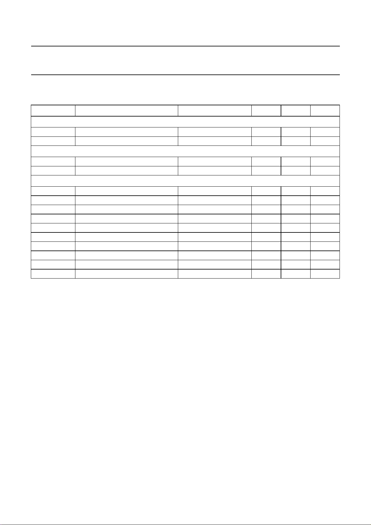
8.4 Bus timing Table 24 Digital levels and timing
SYMBOL PARAMETER CONDITIONS MIN. MAX. UNIT
Digital inputs
V
IH
V
IL
Digital outputs
I
sink(L)
V
OL
Timing (3-wire bus enabled)
f
clk
t
HIGH
t
LOW
t
W(write)
t
W(read)
t
su(clk)
t
h(out)
t
d(out)
t
su(write)
t
h(write)
HIGH-level input voltage 0.45V
LOW-level input voltage − 0.2V
CCD
− V
CCD
LOW-level sink current 500 −µA
LOW-level output voltage IOL= 500 µA − 450 mV
clock input frequency − 400 kHz
clock HIGH time 1 −µs
clock LOW time 1 −µs
pulse width for write enable 1 −µs
pulse width for read enable 1 −µs
clock set-up time 300 − ns
read mode data output hold time 10 − ns
read mode output delay time − 400 ns
write mode set-up time 100 − ns
write mode hold time 100 − ns
V
2004 Sep 13 14
Page 15
Philips Semiconductors Product specification
Low-power FM stereo radio for
TEA5767HL
handheld applications
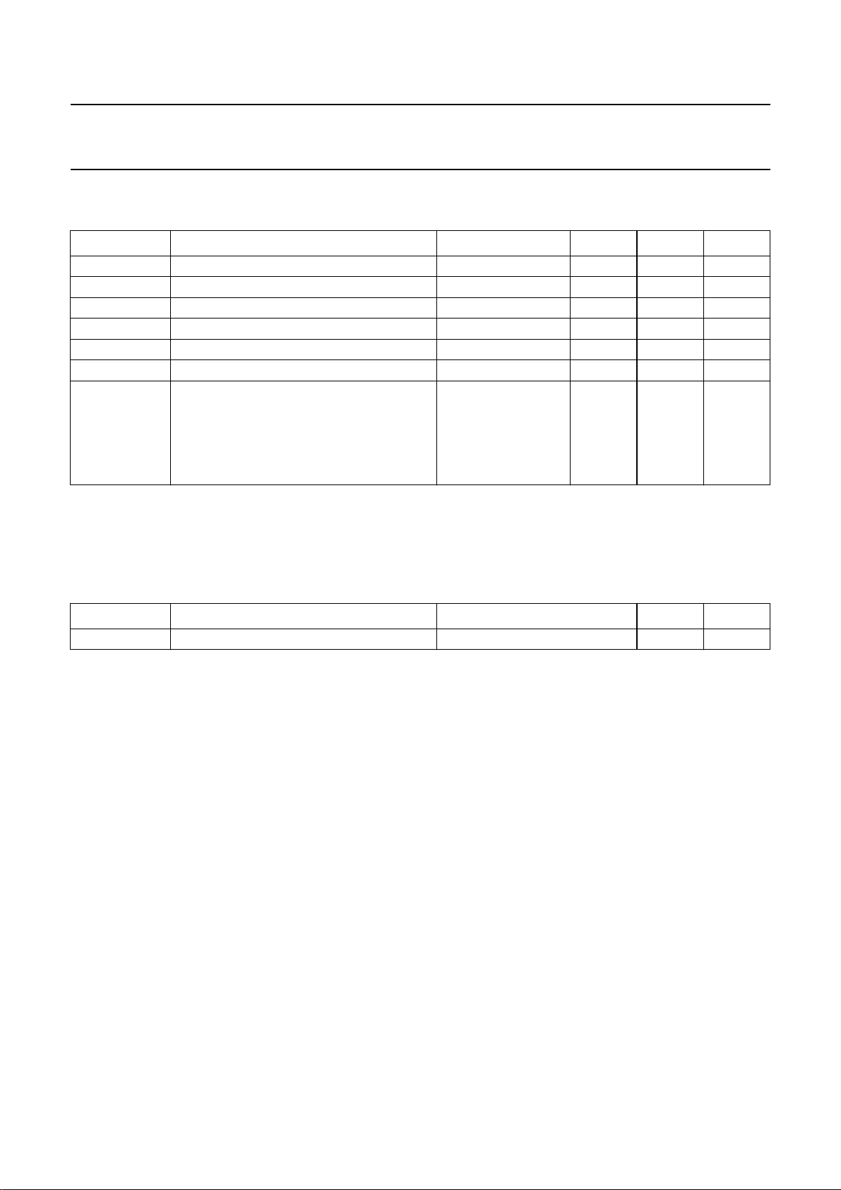
9 LIMITING VALUES
In accordance with the Absolute Maximum Rating System (IEC 60134).
SYMBOL PARAMETER CONDITIONS MIN. MAX. UNIT
V
VCOTANK1
V
VCOTANK2
V
CCD
V
CCA
T
stg
T
amb
V
es
Notes
1. Machine model (R = 0 Ω, C = 200 pF).
2. Human body model (R = 1.5 kΩ, C = 100 pF).
VCO tuned circuit output voltage 1 −0.3 +8 V
VCO tuned circuit output voltage 2 −0.3 +8 V
digital supply voltage −0.3 +5 V
analog supply voltage −0.3 +8 V
storage temperature −55 +150 °C
ambient temperature −10 +75 °C
electrostatic handling voltage
for all pins except pin DATA note 1 −200 +200 V
note 2 −2000 +2000 V
for pin DATA note 1 −150 +200 V
note 2 −2000 +2000 V
10 THERMAL CHARACTERISTICS
SYMBOL PARAMETER CONDITIONS VALUE UNIT
R
th(j-a)
thermal resistance from junction to ambient in free air 80 K/W
2004 Sep 13 15
Page 16
Philips Semiconductors Product specification
Low-power FM stereo radio for
TEA5767HL
handheld applications
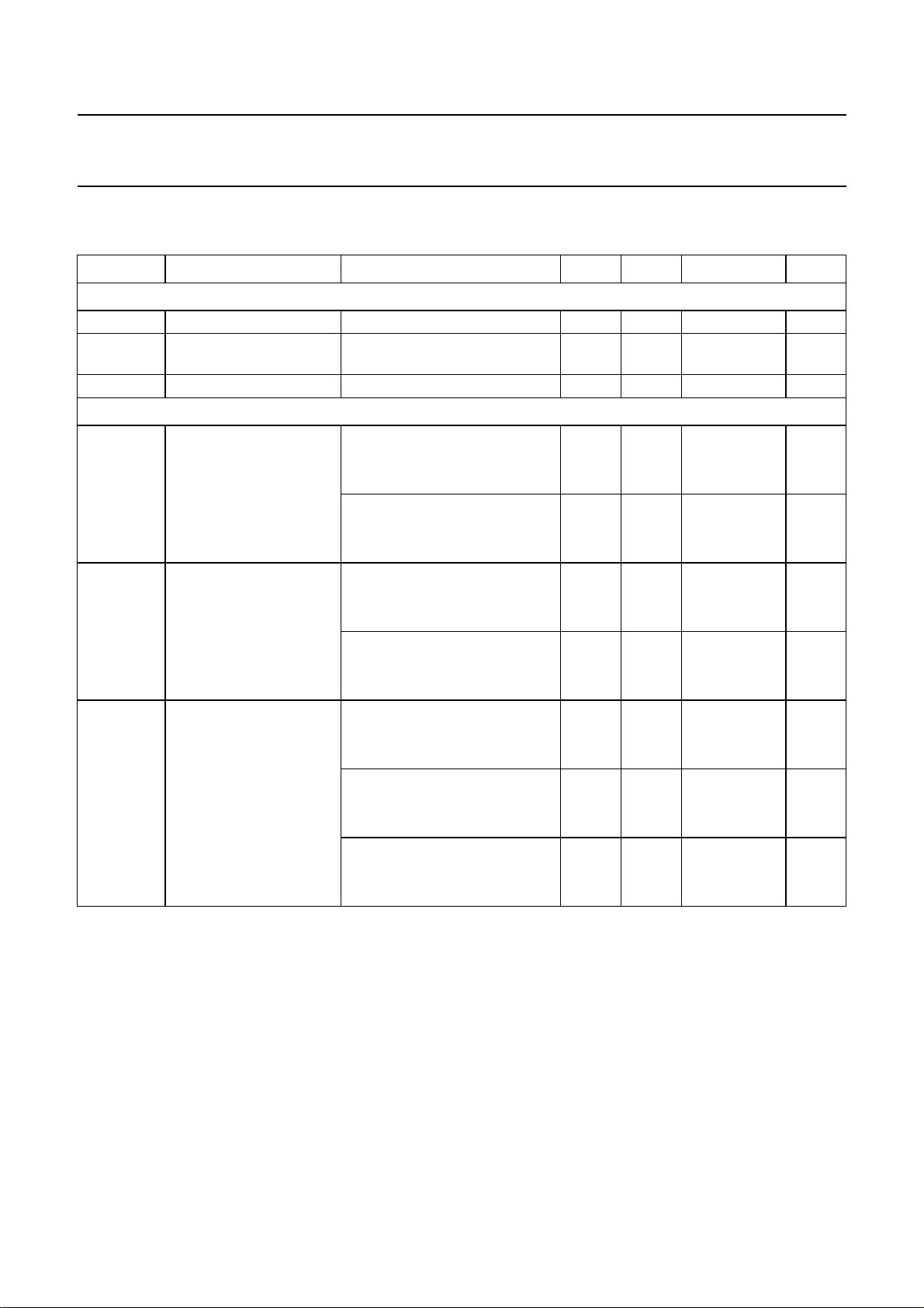
11 DC CHARACTERISTICS
V
CCA=VVCOTANK1=VVCOTANK2=VCCD
SYMBOL PARAMETER CONDITIONS MIN. TYP. MAX. UNIT
Supply voltages; note 1
V
CCA
V
CC(VCO)
analog supply voltage 2.5 3.0 5.0 V
voltage controlled
oscillator supply voltage
V
CCD
digital supply voltage 2.5 3.0 5.0 V
Supply currents
I
CCA
I
CC(VCO)
analog supply current operating
voltage controlled
oscillator supply current
I
CCD
digital supply current operating
= 2.7 V; T
=25°C; unless otherwise specified.
amb
2.5 3.0 5.0 V
V
= 3 V 6.0 8.4 10.5 mA
CCA
V
= 5 V 6.2 8.6 10.7 mA
CCA
standby mode
V
=3V − 36 µA
CCA
V
=5V − 3.2 6.2 µA
CCA
operating
V
VCOTANK1=VVCOTANK2
V
VCOTANK1=VVCOTANK2
= 3 V 560 750 940 µA
= 5 V 570 760 950 µA
standby mode
V
VCOTANK1=VVCOTANK2
V
VCOTANK1=VVCOTANK2
V
= 3 V 2.1 3.0 3.9 mA
CCD
V
= 5 V 2.25 3.15 4.05 mA
CCD
standby mode; V
CCD
=3V − 12 µA
=5V − 1.2 2.2 µA
=3V
bus enable line HIGH 30 56 80 µA
bus enable line LOW 11 19 26 µA
standby mode; V
CCD
=5V
bus enable line HIGH 50 78 105 µA
bus enable line LOW 20 33 45 µA
2004 Sep 13 16
Page 17
Philips Semiconductors Product specification
Low-power FM stereo radio for
TEA5767HL
handheld applications
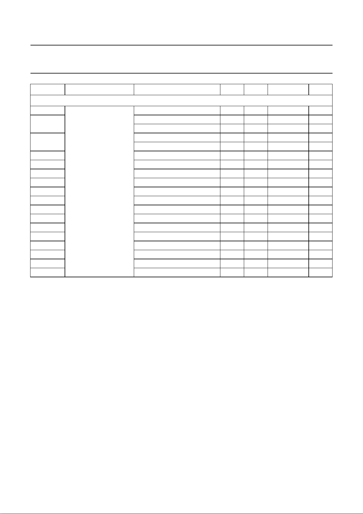
SYMBOL PARAMETER CONDITIONS MIN. TYP. MAX. UNIT
DC operating points
V
CPOUT
V
XTAL1
V
XTAL2
V
PHASEFIL
V
PILFIL
V
VAFL
V
VAFR
V
TMUTE
V
MPXO
V
Vref
V
TIFC
V
LIMDEC1
V
LIMDEC2
V
Igain
V
RFI1
V
RFI2
V
TAGC
Note
1. V
CCA
unloaded DC voltage 0.1 − V
data byte 4 bit 4 = 1 1.64 1.72 1.8 V
data byte 4 bit 4 = 0 1.68 1.75 1.82 V
data byte 4 bit 4 = 1 1.64 1.72 1.8 V
data byte 4 bit 4 = 0 1.68 1.75 1.82 V
0.4 1.2 V
0.65 0.9 1.3 V
fRF= 98 MHz; VRF= 1 mV 720 850 940 mV
fRF= 98 MHz; VRF= 1 mV 720 850 940 mV
VRF= 0 V 1.5 1.65 1.8 V
fRF= 98 MHz; VRF= 1 mV 680 815 950 mV
1.45 1.55 1.65 V
1.34 1.44 1.54 V
1.86 1.98 2.1 V
1.86 1.98 2.1 V
480 530 580 mV
0.93 1.03 1.13 V
0.93 1.03 1.13 V
VRF= 0 V 1 1.57 2 V
, V
CC(VCO)
and V
must not differ more than 200 mV.
CCD
CC(VCO)
− 0.4 V
CCA
− 0.1 V
2004 Sep 13 17
Page 18
Philips Semiconductors Product specification
Low-power FM stereo radio for
TEA5767HL
handheld applications
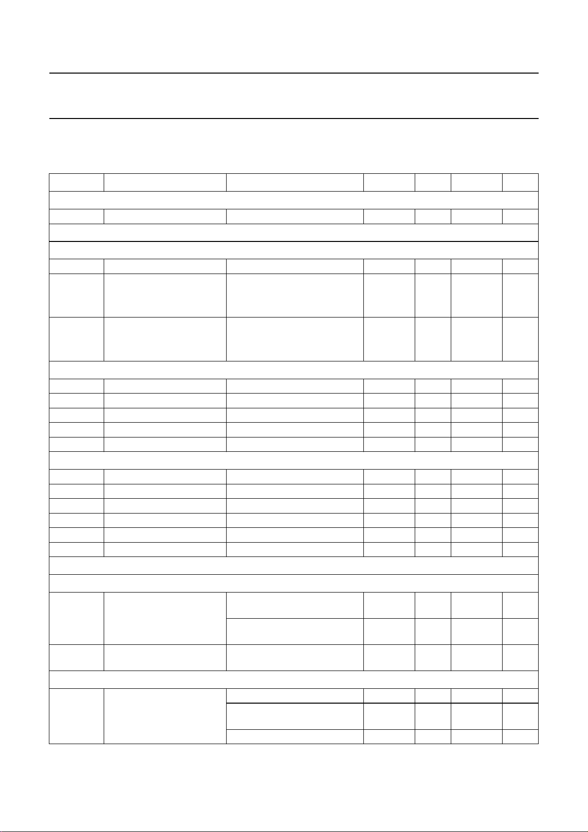
12 AC CHARACTERISTICS
V
CCA=VVCOTANK1=VVCOTANK2=VCCD
in RMS; unless otherwise specified.
SYMBOL PARAMETER CONDITIONS MIN. TYP. MAX. UNIT
Voltage controlled oscillator
f
osc
oscillator frequency 150 − 217 MHz
Crystal oscillator
C
IRCUIT INPUT: PIN XTAL2
V
R
C
i(osc)
i
i
oscillator input voltage oscillator externally clocked 140 − 350 mV
input resistance oscillator externally clocked
input capacitance oscillator externally clocked
CRYSTAL: 32.768 kHz
f
r
∆f/f
C
0
R
S
∆fr/f
r
r(25 °C)
series resonance frequency data byte 4 bit 4 = 1 − 32.768 − kHz
frequency deviation −20 × 10−6− +20 × 10
shunt capacitance −−3.5 pF
series resistance −−80 kΩ
temperature drift −10 °C<T
CRYSTAL:13MHZ
f
r
∆f/f
C
0
C
mot
R
S
∆fr/f
r
r(25 °C)
series resonance frequency data byte 4 bit 4 = 0 − 13 − MHz
frequency deviation −30 × 10−6− +30 × 10
shunt capacitance −−4.5 pF
motional capacitance 1.5 − 3.0 fF
series resistance −−100 Ω
temperature drift −40 °C<T
Synthesizer
= 2.7 V; T
=25°C; measured in the circuit of Fig.7; all AC values are given
amb
data byte 4 bit 4 = 0 2 3 4 kΩ
data byte 4 bit 4 = 1 230 330 430 kΩ
data byte 4 bit 4 = 0 3.9 5.6 7.3 pF
data byte 4 bit 4 = 1 5 6 7 pF
< +60 °C −50 × 10−6− +50 × 10
amb
< +85 °C −30 × 10−6− +30 × 10
amb
−6
−6
−6
−6
PROGRAMMABLE DIVIDER; note 1
N
prog
programmable divider ratio data byte 1 = XX111111;
data byte 2 = 11111110
data byte 1 = XX010000;
data byte 2 = 00000000
∆N
step
programmable divider step
size
REFERENCE FREQUENCY DIVIDER
N
ref
crystal oscillator divider
ratio
data byte 4 bit 4 = 0 − 260 −
data byte 5 bit 7 = 1;
data byte 4 bit 4 = 0
data byte 4 bit 4 = 1 − 1 −
2004 Sep 13 18
−−8191
2048 −−
− 1 −
− 130 −
Page 19
Philips Semiconductors Product specification
Low-power FM stereo radio for
TEA5767HL
handheld applications
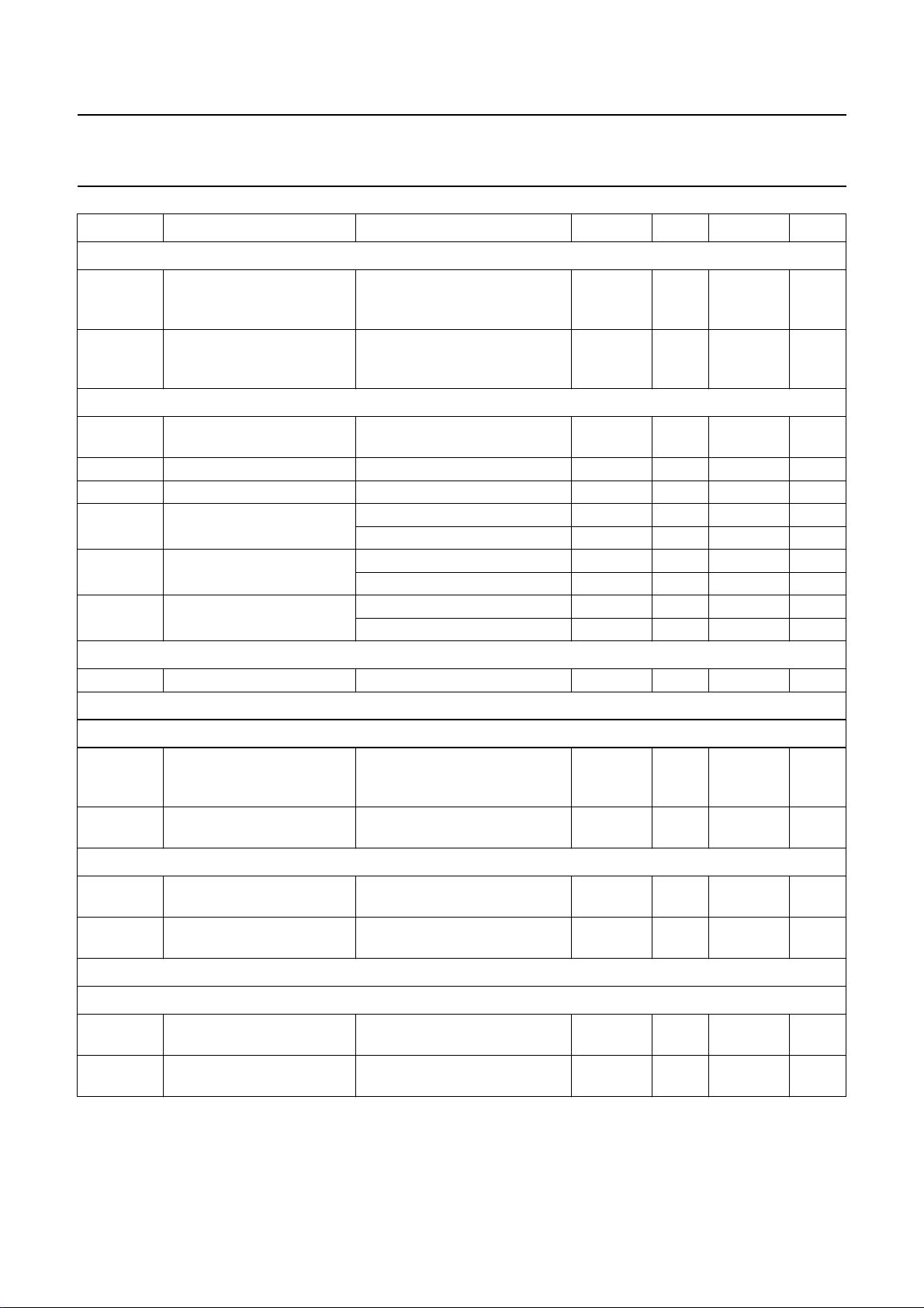
SYMBOL PARAMETER CONDITIONS MIN. TYP. MAX. UNIT
CHARGE PUMP: PIN CPOUT
I
sink
I
source
IF counter
V
RF
N
IF
N
precount
T
count(IF)
RES
count(IF)
IF
count
Pins DATA, CLOCK, WRITE/READ and BUSENABLE
R
i
Software programmable ports
charge pump peak sink
current
charge pump peak source
current
RF input voltage for correct
0.2V<V
<V
VCOTANK2
f
VCO>fref
0.2V<V
<V
VCOTANK2
f
VCO<fref
CPOUT
− 0.2 V;
× N
CPOUT
− 0.2 V;
× N
− 0.5 −µA
prog
−−0.5 −µA
prog
− 12 18 µV
IF count
IF counter length − 7 − bit
IF counter prescaler ratio − 64 −
IF counter period f
IF counter resolution f
IF counter result for search
tuning stop
= 32.768 kHz − 15.625 − ms
xtal
f
= 13 MHz − 15.754 − ms
xtal
= 32.768 kHz − 4.096 − kHz
xtal
f
= 13 MHz − 4.0625 − kHz
xtal
f
= 32.768 kHz 31 − 3E HEX
xtal
f
= 13 MHz 32 − 3D HEX
xtal
input resistance 10 −− MΩ
PIN SWPORT1
I
sink(max)
I
leak(max)
maximum sink current data byte 3 bit 0 = 0;
maximum leakage current data byte 3 bit 0 = 1;
PIN SWPORT2
I
sink(max)
I
leak(max)
maximum sink current data byte 4 bit 7 = 0;
maximum leakage current data byte 4 bit 7 = 1;
FM signal channel
FM RF INPUT
R
i
input resistance at pins
RFI1 and RFI2 to RFGND
C
i
input capacitance at pins
RFI1 and RFI2 to RFGND
data byte 4 bit 0 = 0;
V
SWPORT1
V
SWPORT1
V
SWPORT1
V
SWPORT1
< 0.5 V
<5V
< 0.5 V
<5V
500 −− µA
−1 − +1 µA
500 −− µA
−1 − +1 µA
75 100 125 Ω
2.5 4 6 pF
2004 Sep 13 19
Page 20
Philips Semiconductors Product specification
Low-power FM stereo radio for
TEA5767HL
handheld applications
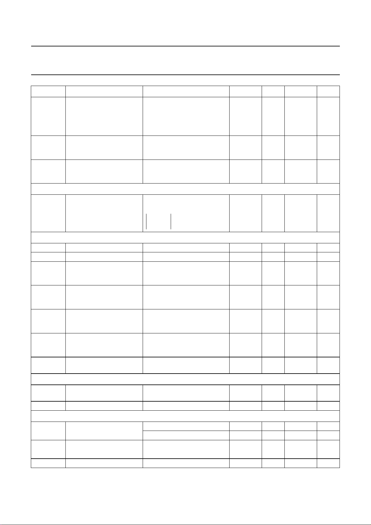
SYMBOL PARAMETER CONDITIONS MIN. TYP. MAX. UNIT
V
RF
IP3
in
IP3
out
RF AGC
V
RF1
IF filter
f
IF
B
IF
S
+200
S
−200
S
+100
S
−100
IR image rejection f
FM IF level detector and mute voltage
V
RF
∆V
step
PIN TMUTE
V
level
V
level(slope)
R
o
RF sensitivity input voltage fRF= 76 MHz to 108 MHz;
∆f = 22.5 kHz; f
mod
= 1 kHz;
− 2 3.5 µV
(S+N)/N = 26 dB;
de-emphasis = 75 µs;
BAF= 300 Hz to 15 kHz
in-band 3rd-order intercept
point related to V
RFI1-RFI2
∆f1= 200 kHz; ∆f2= 400 kHz;
f
= 76 MHz to 108 MHz
tune
81 84 − dBµV
(peak value)
out-band 3rd-order
intercept point related to
V
RFI1-RFI2
(peak value)
RF input voltage for start of
AGC
∆f1= 4 MHz; ∆f2= 8 Hz;
f
= 76 MHz to 108 MHz
tune
f
= 93 MHz; f
RF1
V
=50dBµV;
RF2
V
∆
TMUTE
----------------------V
RF1
<
RF2
14 mV
-------------------3 dBµV
= 98 MHz;
; note 2
82 85 − dBµV
66 72 78 dBµV
IF filter centre frequency 215 225 235 kHz
IF filter bandwidth 85 94 102 kHz
HIGH side 200 kHz
selectivity
∆f = +200 kHz;
f
= 76 MHz to 108 MHz;
tune
39 43 − dB
note 3
LOW side 200 kHz
selectivity
∆f=−200 kHz;
f
= 76 MHz to 108 MHz;
tune
32 36 − dB
note 3
HIGH side 100 kHz
selectivity
∆f = +100 kHz;
f
= 76 MHz to 108 MHz;
tune
812− dB
note 3
LOW side 100 kHz
selectivity
∆f=−100 kHz;
f
= 76 MHz to 108 MHz;
tune
812− dB
note 3
= 76 MHz to 108 MHz;
tune
24 30 − dB
VRF=50dBµV
RF input voltage for start of
read mode data byte 4 bit4=1 2 3 5 µV
level ADC
level ADC step size 2 3 5 dB
level output DC voltage VRF=0µV 1.55 1.65 1.80 V
VRF=3µV 1.60 1.70 1.85 V
slope of level voltage VRF=10µV to 500 µV 150 165 180
mV
--------------20 dB
output resistance 280 400 520 kΩ
2004 Sep 13 20
Page 21
Philips Semiconductors Product specification
Low-power FM stereo radio for
TEA5767HL
handheld applications
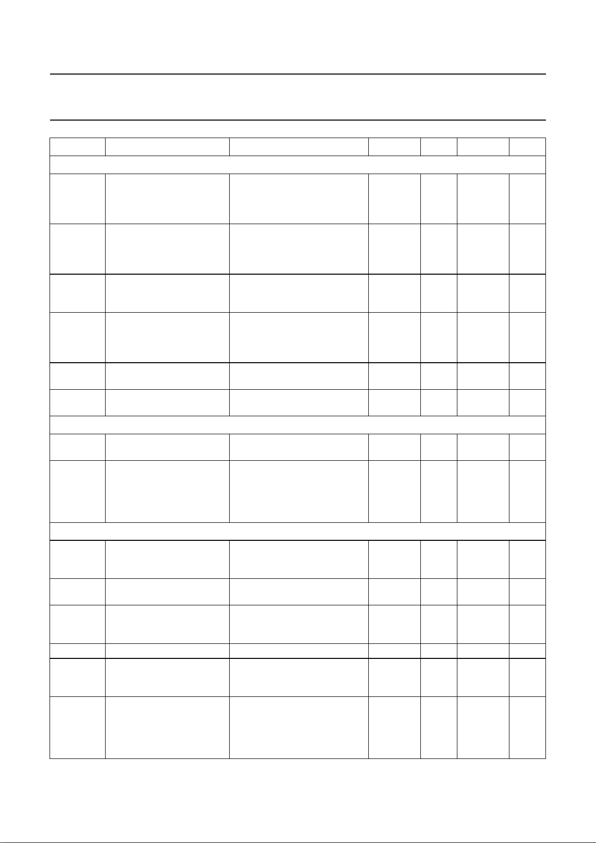
SYMBOL PARAMETER CONDITIONS MIN. TYP. MAX. UNIT
FM demodulator: pin MPXO
V
MPXO
(S+N)/N maximum signal plus
THD total harmonic distortion VRF= 1 mV;L = R; ∆f = 75 kHz;
α
AM
R
o
I
sink
Soft mute
V
RF
α
mute
MPX decoder
V
; V
AFL
R
; R
AFL
I
sink(AFL)
I
sink(AFR)
V
MPXIN(max)
V
AFL/VAFR
α
cs(stereo)
demodulator output voltage VRF= 1 mV; L = R;
∆f = 22.5 kHz; f
mod
= 1 kHz;
60 75 90 mV
de-emphasis = 75 µs;
BAF= 300 Hz to 15 kHz
noise-to-noise ratio
VRF= 1 mV; L = R;
∆f = 22.5 kHz; f
mod
= 1 kHz;
54 60 − dB
de-emphasis = 75 µs;
BAF= 300 Hz to 15 kHz
− 0.5 1.5 %
f
= 1 kHz;
mod
de-emphasis = 75 µs
AM suppression VRF= 300 µV; L=R;
∆f = 22.5 kHz; f
mod
= 1 kHz;
40 −− dB
m = 0.3; de-emphasis = 75 µs;
BAF= 300 Hz to 15 kHz
demodulator output
−−500 Ω
resistance
demodulator output sink
−−30 µA
current
RF input voltage for soft
mute start
mute attenuation VRF=1µV; L = R;
α
= 3 dB; data byte 4
mute
bit3=1
∆f = 22.5 kHz; f
mod
3510µV
10 20 30 dB
= 1 kHz
de-emphasis = 75 µs;
BAF= 300 Hz to 15 kHz;
data byte 4 bit 3 = 1
left and right audio
AFR
frequency output voltage
VRF= 1 mV; L = R;
∆f = 22.5 kHz; f
mod
60 75 90 mV
= 1 kHz;
de-emphasis = 75 µs
left and right audio
AFR
−−50 Ω
frequency output resistance
;
left and right audio
170 −− µA
frequency output sink
current
input overdrive margin THD < 3 % 4 −− dB
left and right audio
frequency output voltage
difference
stereo channel separation VRF= 1 mV; R = L = 0 or R = 0
VRF= 1 mV;L = R; ∆f = 75 kHz;
f
= 1 kHz;
mod
de-emphasis = 75 µs
−1 − +1 dB
24 30 − dB
and L = 1 including 9 % pilot;
∆f = 75 kHz; f
mod
= 1 kHz;
data byte 3 bit 3 = 0;
data byte 4 bit 1 = 1
2004 Sep 13 21
Page 22
Philips Semiconductors Product specification
Low-power FM stereo radio for
TEA5767HL
handheld applications
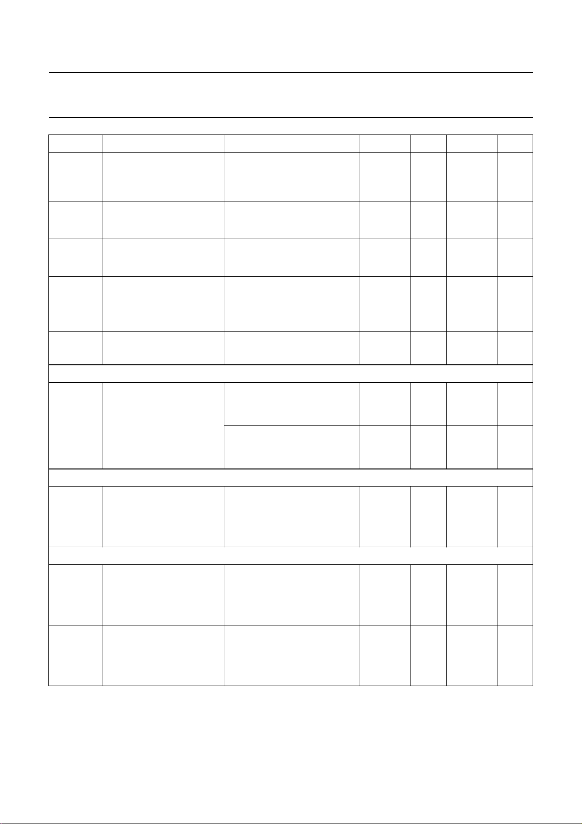
SYMBOL PARAMETER CONDITIONS MIN. TYP. MAX. UNIT
(S+N)/N maximum signal plus
noise-to-noise ratio
THD total harmonic distortion VRF= 1 mV;L = R; ∆f = 75 kHz;
α
∆f
pilot
pilot
pilot suppression measured
at pins V
AFL
and V
AFR
stereo pilot frequency
deviation
f
∆
pilot1
--------------- f
∆
pilot2
pilot switch hysteresis VRF= 1 mV 2 −− dB
VRF= 1 mV; L = R;
∆f = 22.5 kHz; f
mod
= 1 kHz;
54 60 − dB
de-emphasis = 75 µs;
BAF= 300 Hz to 15 kHz
− 0.4 1 %
f
= 1 kHz;
mod
de-emphasis = 75 µs
related to ∆f = 75 kHz;
f
= 1 kHz;
mod
40 50 − dB
de-emphasis = 75 µs
VRF= 1 mV; read mode;
data byte 3
bit7=1 − 3.6 5.8 kHz
bit7=0 1 3 − kHz
HIGH CUT CONTROL
TC
de-em
de-emphasis time constant VRF=1mV
MONO TO STEREO BLEND CONTROL
α
cs(stereo)
stereo channel separation VRF=45µV;R=L=0orR=0
MONO TO STEREO SWITCHED
α
cs(stereo)
stereo channel separation
switching from mono to
stereo with increasing RF
input level
α
cs(stereo)
stereo channel separation
switching from stereo to
mono with decreasing RF
input level
data byte 5 bit 6 = 0 38 50 62 µs
data byte 5 bit 6 = 1 57 75 93 µs
VRF=1µV
data byte 5 bit 6 = 0 114 150 186 µs
data byte 5 bit 6 = 1 171 225 279 µs
41016dB
and L = 1 including 9 % pilot;
∆f = 75 kHz; f
mod
= 1 kHz;
data byte 3 bit 3 = 0;
data byte 4 bit 1 = 1
VRF= 1 mV; R = L = 0 or R = 0
24 −− dB
and L = 1 including 9 % pilot;
∆f = 75 kHz; f
mod
= 1 kHz;
data byte 3 bit 3 = 0;
data byte 4 bit 1 = 0
VRF=20µV;R=L=0orR=0
−−1dB
and L = 1 including 9 % pilot;
∆f = 75 kHz; f
mod
= 1 kHz;
data byte 3 bit 3 = 0;
data byte 4 bit 1 = 0
2004 Sep 13 22
Page 23
Philips Semiconductors Product specification
Low-power FM stereo radio for
TEA5767HL
handheld applications
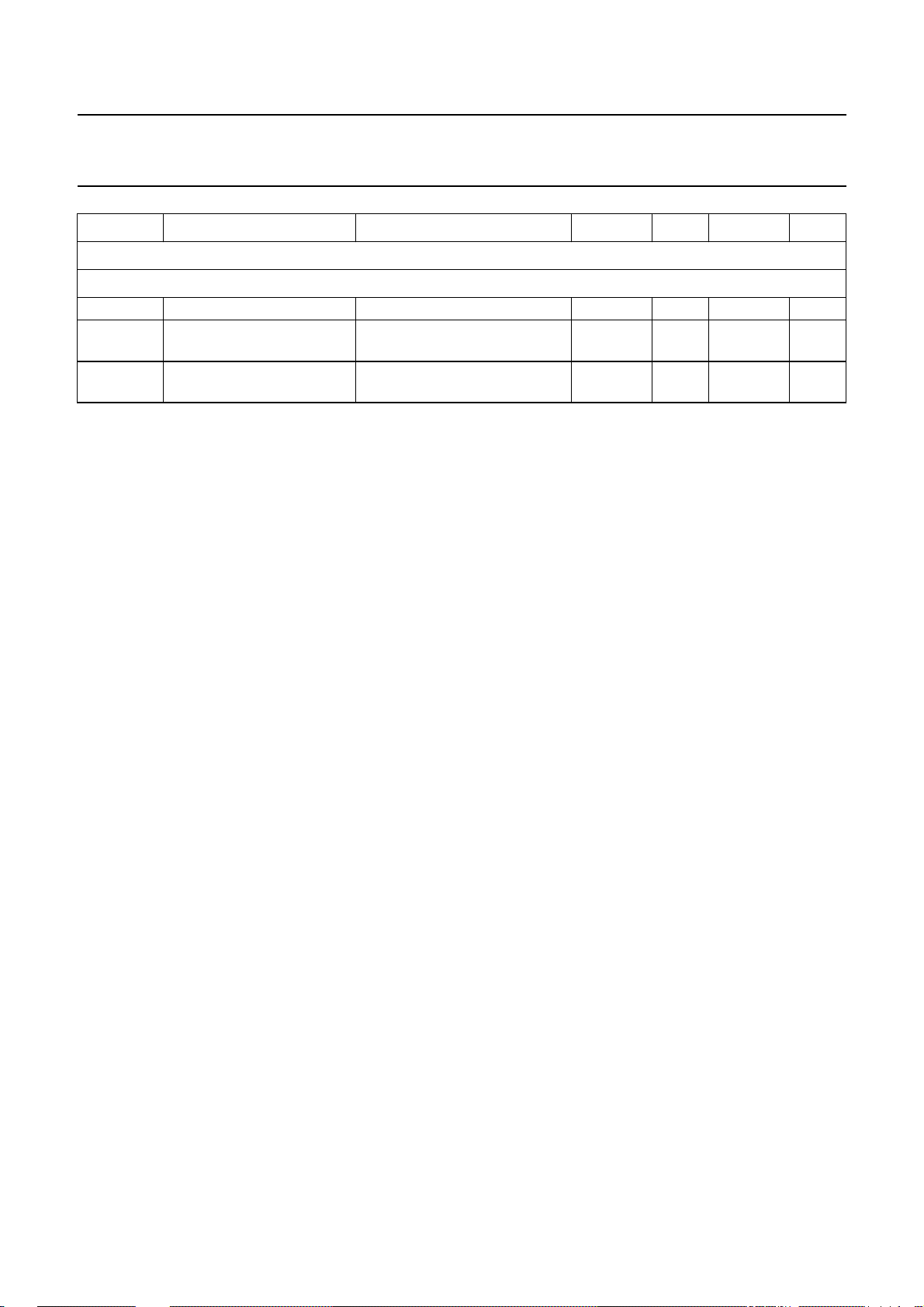
SYMBOL PARAMETER CONDITIONS MIN. TYP. MAX. UNIT
US-DRIVEN MUTE FUNCTIONS
B
Tuning mute
α
mute
α
mute(L)
α
mute(R)
Notes
1. Calculation of this 14-bit word can be done as follows:
formula for HIGH side injection: ; formula for LOW side injection:
where:
N = decimal value of PLL word
f
RF
= the intermediate frequency [Hz] = 225 kHz
f
IF
f
ref
when externally clocked with 6.5 MHz.
Example for receiving a channel at 100 MHz with HIGH side injection: .
The PLL word becomes 2FCAH.
2. V
RF
3. LOWside andHIGH side selectivitycan be switchedby changing themixer from HIGHside to LOWside LOinjection.
V
and V
AFL
V
muting depth data byte 3 bit 1 = 1;
AFL
V
muting depth data byte 3 bit 2 = 1;
AFR
muting depth data byte 1 bit 7 = 1 −−−60 dB
AFR
−−−80 dB
fAF= 1 kHz; R
load(L)
<30kΩ
−−−80 dB
fAF= 1 kHz; R
4f
= N
N
----------------------------------
+()×
RFfIF
f
ref
load(R)
<30kΩ
= the wanted tuning frequency [Hz]
= the reference frequency [Hz] = 32.768 kHz for the 32.768 kHz crystal; f
N
in Fig.7 is replaced by V
RF1+VRF2
. The radio is tuned to 98 MHz (HIGH side injection).
4f
=
--------------------------------- -
= 50 kHz for the 13 MHz crystal or
ref
4 100
------------------------------------------------------------------
×10 2253×10+()×
32768
6
–()×
RFfIF
f
ref
12234==
2004 Sep 13 23
Page 24
Philips Semiconductors Product specification
Low-power FM stereo radio for
handheld applications
AFL
, V
(dB)
AFR
−
−
−
−
−
−
−
10
0
10
20
30
40
50
60
70
(1)
(2)
(3)
(4)
(5)
(6)
handbook, full pagewidth
V
TEA5767HL
MHC247
THD
(%)
4.0
3.5
3.0
2.5
2.0
1.5
1.0
0.5
−
80
−3
10
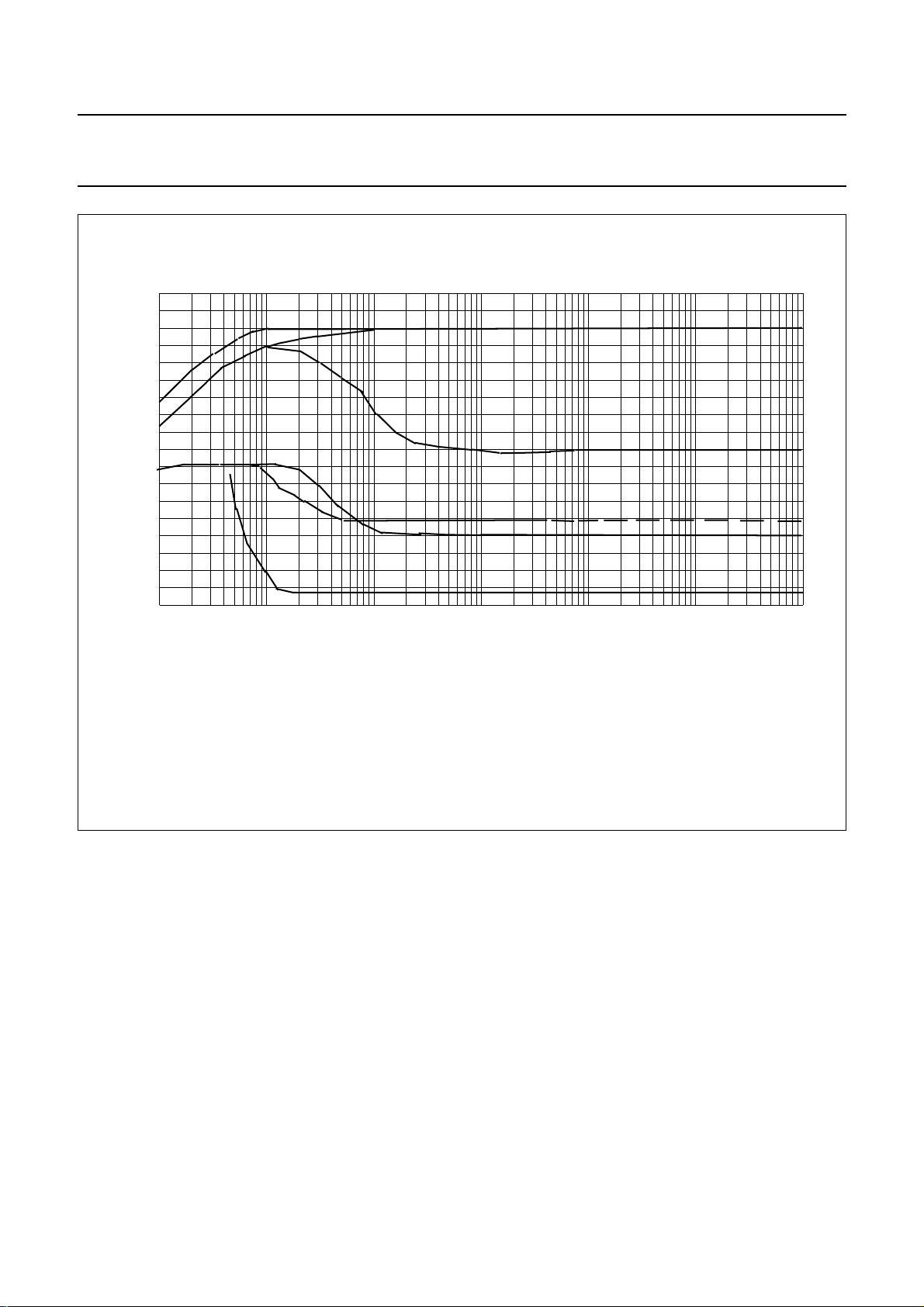
(1) Mono signal; soft mute on.
(2) Left channel with modulation left; SNC on.
(3) Right channel with modulation left; SNC on.
(4) Noise in mono mode; soft mute on.
(5) Noise in stereo mode; SNC on.
(6) Total harmonic distortion; ∆f = 75 kHz; L = R; f
−2
10
−1
mod
10
= 1 kHz.
1
Fig.5 FM characteristics 1.
10 10
2
V
(mV)
RF
0
3
10
2004 Sep 13 24
Page 25
Philips Semiconductors Product specification
Low-power FM stereo radio for
handheld applications
AFL
, V
(dB)
AFR
−
−
−
−
−
−
−
10
0
10
20
30
40
50
60
70
(1)
(2)
(3)
handbook, full pagewidth
V
TEA5767HL
MHC309
V
TMUTE
(V)
2.2
2.1
2.0
1.9
1.8
1.7
1.6
1.5
−
80
−3
10
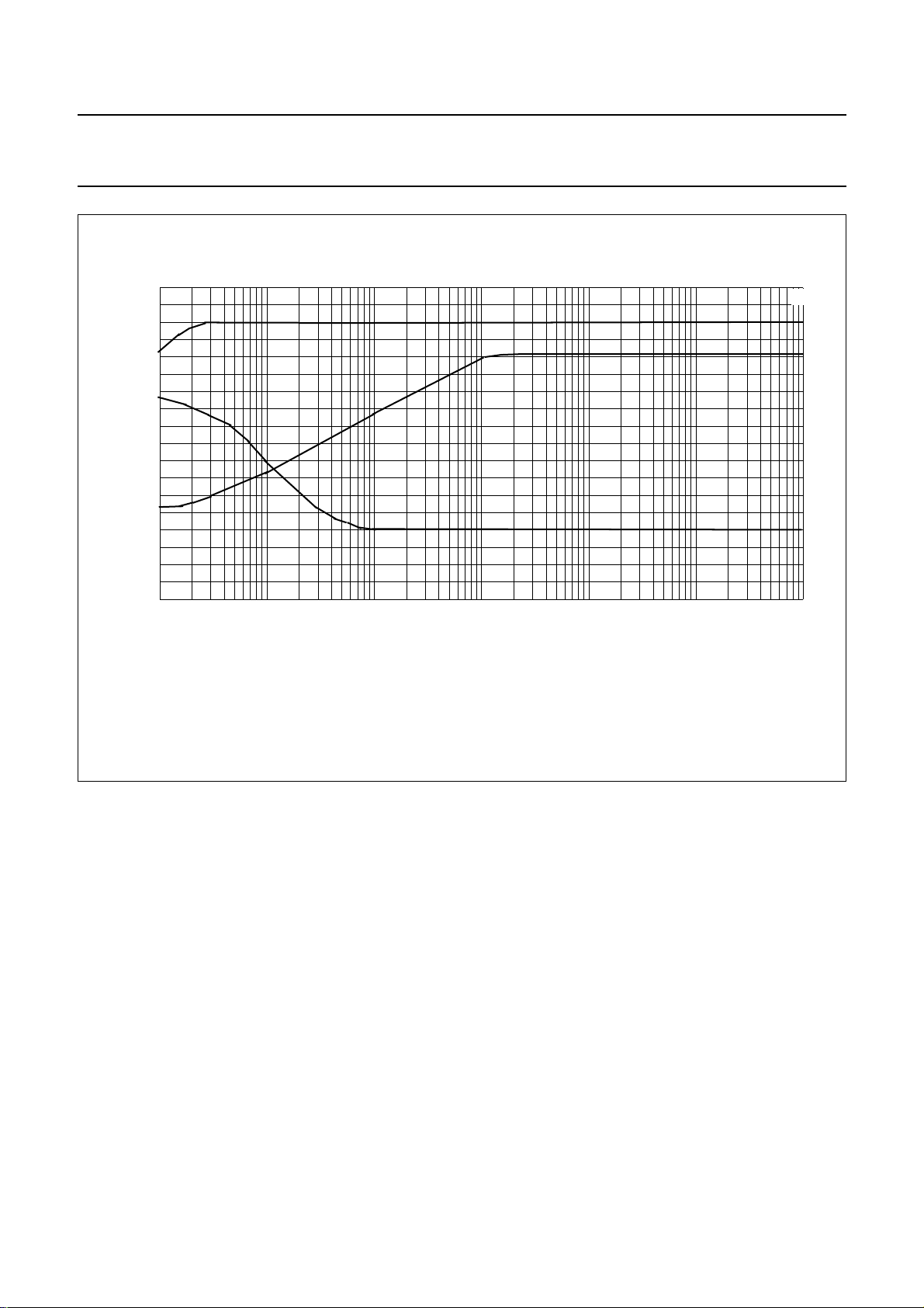
(1) Mono signal; no soft mute.
(2) Noise in mono mode; no soft mute.
(3) Level voltage; V
CCA
= 2.7 V.
−2
10
−1
10
1
Fig.6 FM characteristics 2.
10 10
2
V
(mV)
RF
1.4
3
10
2004 Sep 13 25
Page 26
Philips Semiconductors Product specification
2
3
4
Low-power FM stereo radio for
handheld applications
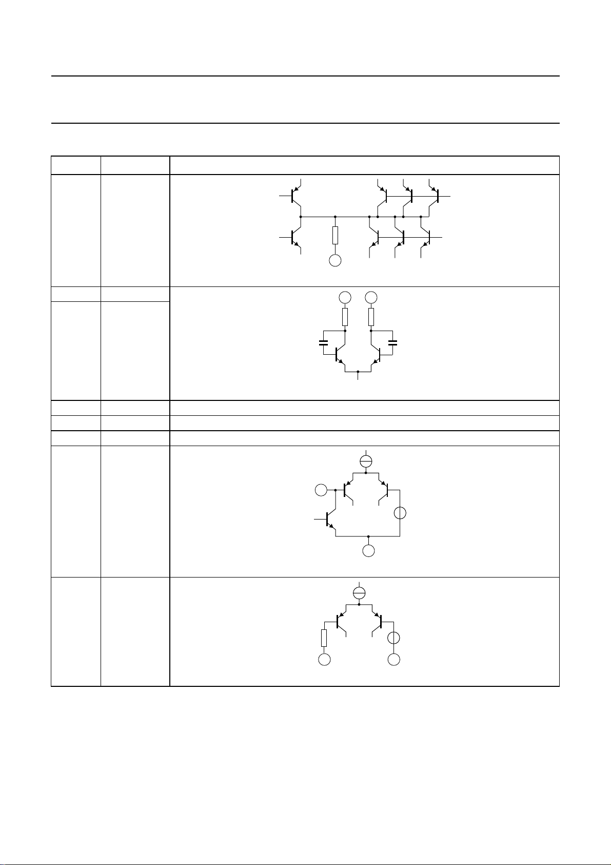
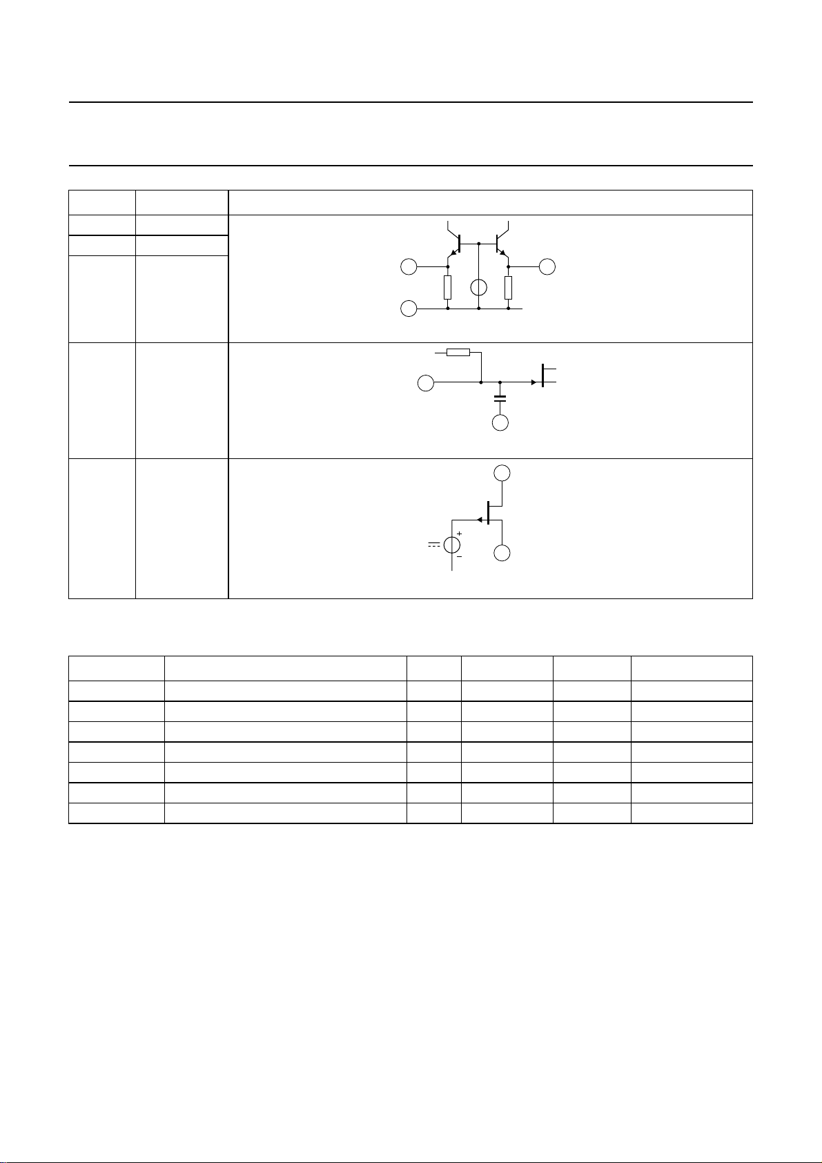
13 INTERNAL PIN CONFIGURATION
PIN SYMBOL EQUIVALENT CIRCUIT
1 CPOUT
270 Ω
1
2 VCOTANK1
3 VCOTANK2
120 Ω
2
3
TEA5767HL
MHC251
120 Ω
MHC25
4V
CC(VCO)
5 DGND
6V
CCD
7 DATA
8 CLOCK
270 Ω
7
5
MHC25
58
MHC25
2004 Sep 13 26
Page 27
Philips Semiconductors Product specification
5
6
7
8
0
Low-power FM stereo radio for
handheld applications
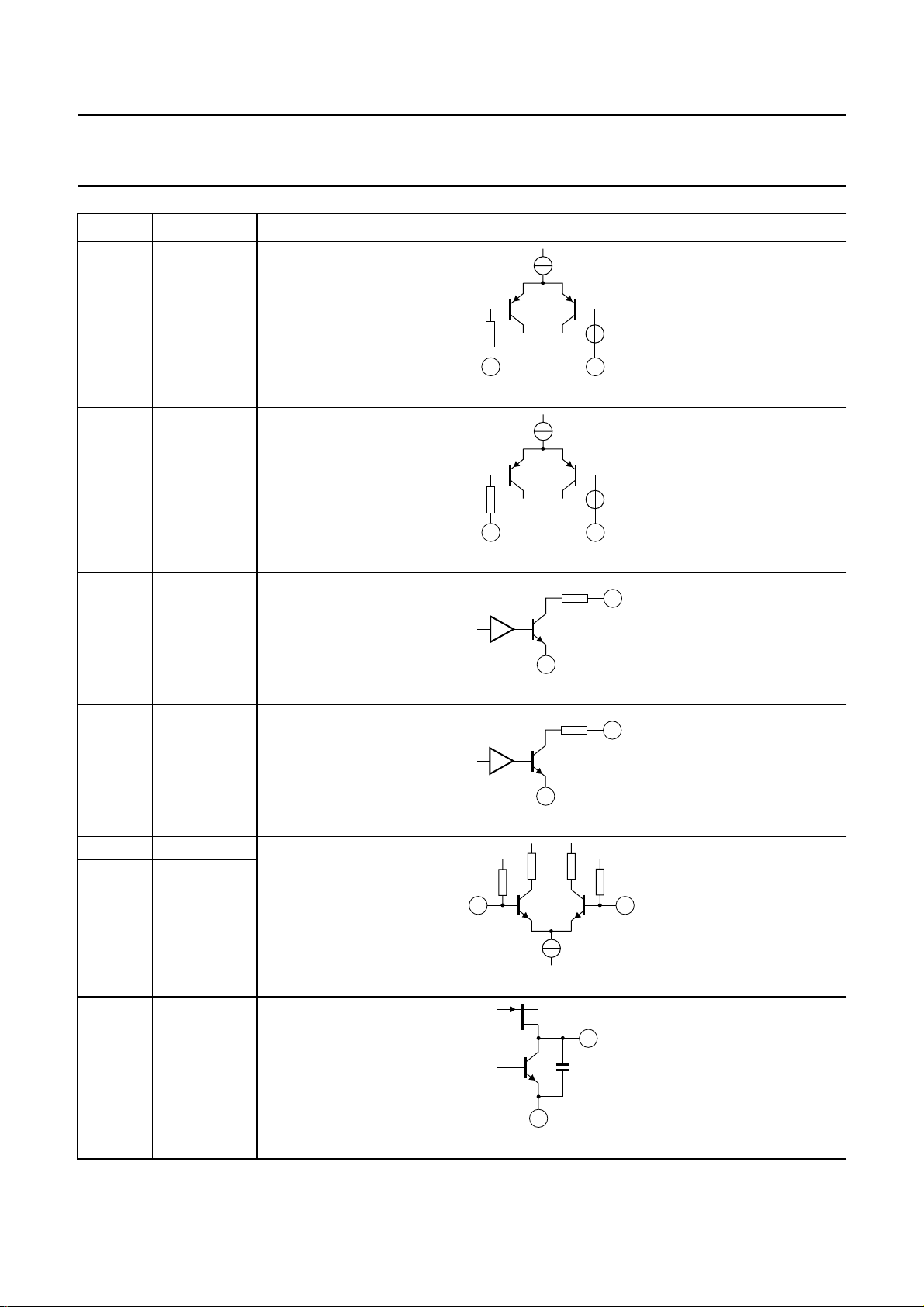
PIN SYMBOL EQUIVALENT CIRCUIT
9 WRITE/READ
270 Ω
10 BUSENABLE
150 Ω
11 SWPORT1
150 Ω
TEA5767HL
59
MHC25
510
MHC25
11
12 SWPORT2
13 XTAL1
14 XTAL2
15 PHASEFIL
5
5
13 14
150 Ω
MHC25
12
MHC25
MHC259
15
2004 Sep 13 27
26
MHC26
Page 28
Philips Semiconductors Product specification
4
Low-power FM stereo radio for
handheld applications
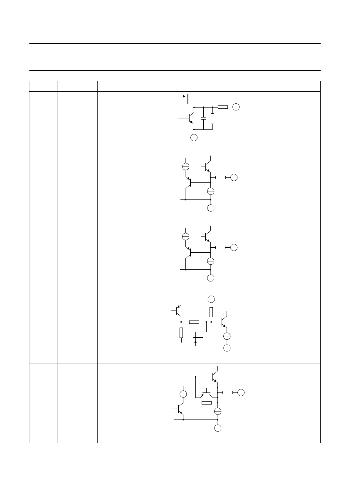
PIN SYMBOL EQUIVALENT CIRCUIT
16 PILFIL
270 Ω
26
17 V
AFL
10 Ω
26
TEA5767HL
16
MHC261
17
MHC262
18 V
AFR
19 TMUTE
20 MPXO
10 Ω
18
26
MHC263
19
1 kΩ
26
MHC26
150 Ω
20
2004 Sep 13 28
26
MHC265
Page 29
Philips Semiconductors Product specification
7
8
9
0
Low-power FM stereo radio for
handheld applications
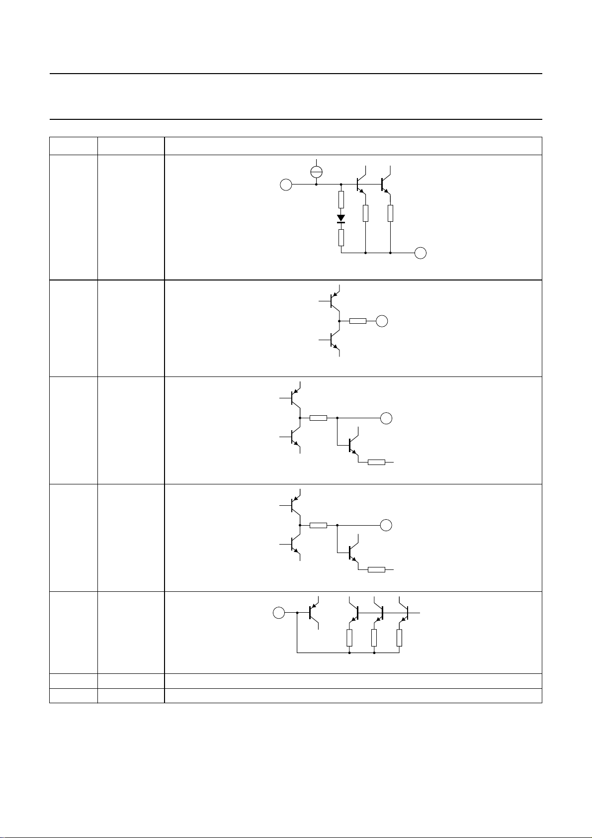
PIN SYMBOL EQUIVALENT CIRCUIT
21 V
22 TIFC
ref
21
MHC266
40 kΩ
MHC26
TEA5767HL
26
22
23 LIMDEC1
24 LIMDEC2
25 I
gain
270 Ω
270 Ω
25
23
MHC26
24
MHC26
MHC27
26 AGND
27 V
CCA
2004 Sep 13 29
Page 30
Philips Semiconductors Product specification
2
3
Low-power FM stereo radio for
handheld applications
PIN SYMBOL EQUIVALENT CIRCUIT
28 RFI1
29 RFGND
30 RFI2
31 TAGC
32 LOOPSW
28 30
29
31
29
4
TEA5767HL
MHC271
MHC27
32
MHC27
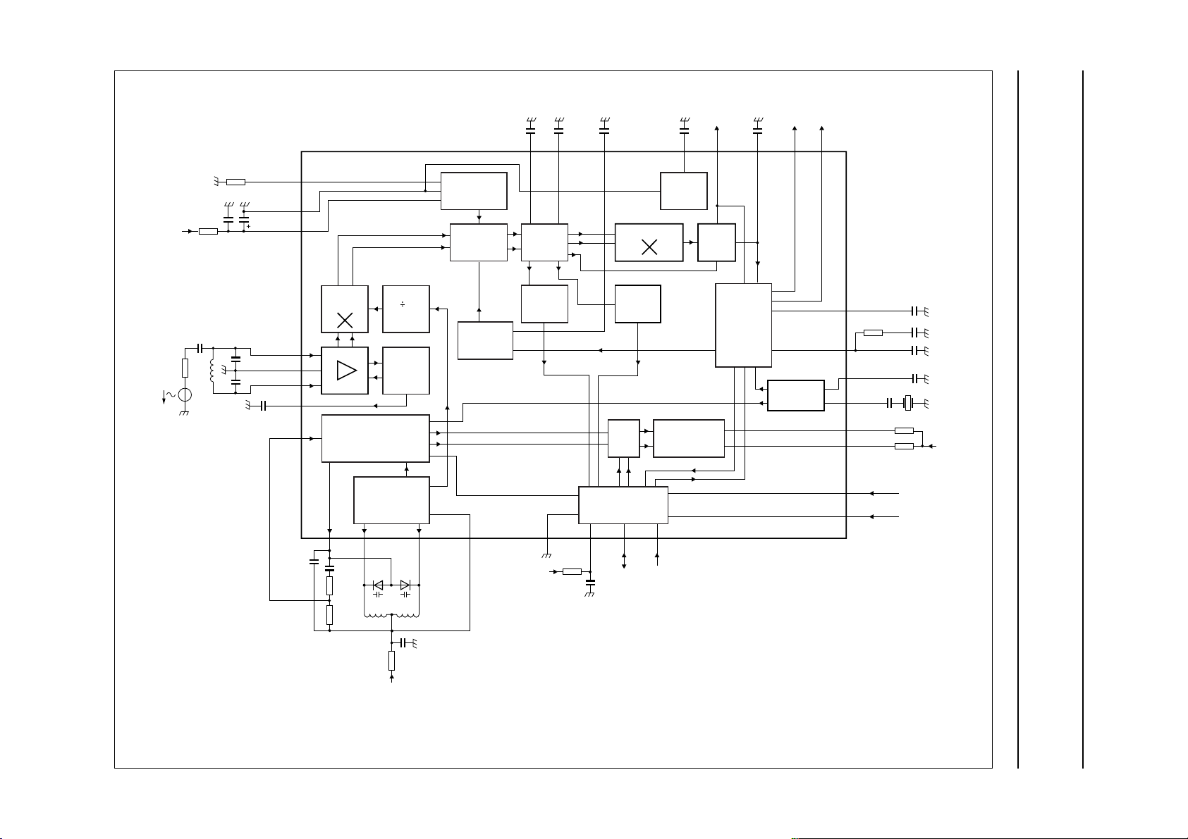
14 APPLICATION INFORMATION Table 25 Component list for Figs 1 and 7
COMPONENT PARAMETER VALUE TOLERANCE TYPE MANUFACTURER
R1 resistor with low temperature coefficient 18 kΩ±1 % RC12G Philips
D1 and D2 varicap for VCO tuning −− BB202 Philips
L1 RF band filter coil 120 nH ±2% Q
L2 and L3 VCO coil 33 nH ±2% Q
min
min
=40
=40
XTAL13 13 MHz crystal −− NX4025GA
C
pull
pulling capacitor for NX4025GA 10 pF −
XTAL32.768 32.768 kHz crystal −−
2004 Sep 13 30
Page 31
This text is here in white to force landscape pages to be rotated correctly when browsing through the pdf in the Acrobat reader.This text is here in
_white to force landscape pages to be rotated correctly when browsing through the pdf in the Acrobat reader.This text is here inThis text is here in
white to force landscape pages to be rotated correctly when browsing through the pdf in the Acrobat reader. white to force landscape pages to be ...
2004 Sep 13 31
Philips Semiconductors Product specification
Low-power FM stereo radio for
handheld applications
47 nF 47 nF 33 nF
LIMDEC2
24 23 22 21 20
R1
22 nF
V
CCA
4.7 Ω
100 pF
40 Ω
L1
V
RF
27 pF
47 pF
22 µF
4.7 nF
LOOPSW
I
gain
AGND
V
CCA
RFI1
RFGND
RFI2
TAGC
25
26
27
I/Q-MIXER
1st FM
28
29
30
31
32
TUNING SYSTEM
12
CPOUT VCOTANK2 V
39 nF10 nF
10 kΩ
100 kΩ
VCO
VCOTANK1
D1L3D2
2
N1
AGC
L2
GAIN
STABILIZATION
RESONANCE
AMPLIFIER
IF CENTRE
FREQUENCY
ADJUST
programmable divider output
reference frequency divider output
34
CC(VCO)
LIMDEC1 TIFC V
LIMITER
LEVEL
ADC
5678
DGND CLOCK
12 Ω
V
CCD
47 nF
DEMODULATOR
COUNTER
I
ref
MUX
3-WIRE BUS
CCD
22 nF
IF
TEA5767HL
PROGRAMMABLE
DATAV
ref
POWER
SUPPLY
SOFTWARE
PORT
pilot
mono
MPXO TMUTE
SOFT
MUTE
MPX
DECODER
33 nF
V
AFR
19 18 17
SDS
CRYSTAL
OSCILLATOR
mhc246
V
AFL
16
15
14
13
12
11
10
9
PILFIL
33 kΩ
PHASEFIL
XTAL2
C
pull
XTAL1
SWPORT2
SWPORT1
BUSENABLE
WRITE/READ
1 nF
22 nF
22 nF
(1)
10 kΩ
10 kΩ
C
comp
(1)
32.768 kHz
or
13 MHz
V
CCA
(1) C
comp
and C
data depends on crystal specification.
pull
47 Ω
22 nF
V
CC(VCO)
TEA5767HL
Fig.7 Test circuit.
Page 32
Philips Semiconductors Product specification
Low-power FM stereo radio for
handheld applications
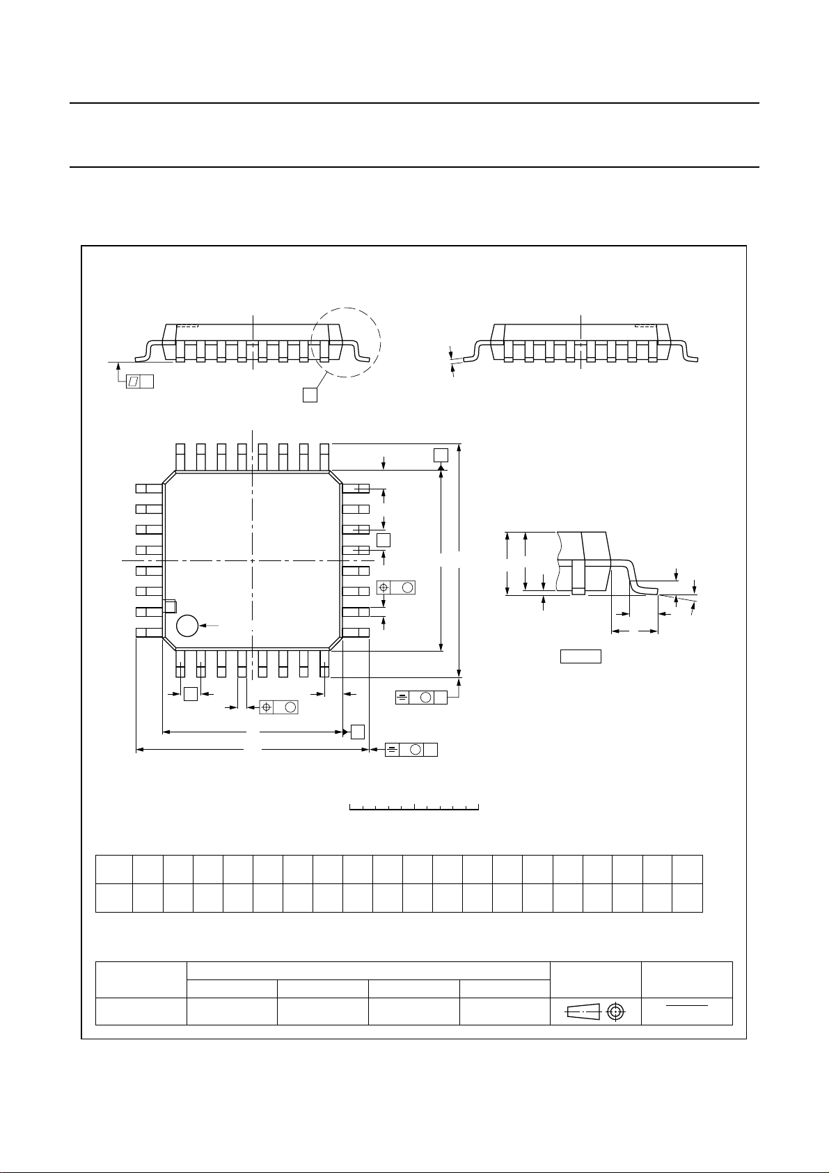
15 PACKAGE OUTLINE
LQFP32: plastic low profile quad flat package; 32 leads; body 7 x 7 x 1.4 mm
c
y
X
24 17
25
16
Z
E
A
TEA5767HL
SOT358-1
e
w
M
b
pin 1 index
32
1
e
DIMENSIONS (mm are the original dimensions)
A
UNIT
mm
Note
1. Plastic or metal protrusions of 0.25 mm maximum per side are not included.
A1A2A3bpcE
max.
0.20
1.45
1.6
0.05
1.35
0.25
w
b
p
M
D
H
D
0.4
0.18
0.3
0.12
8
Z
D
0 2.5 5 mm
(1) (1)(1)
D
7.1
7.1
6.9
6.9
p
9
v
B
v
M
scale
(1)
eHELL
H
9.15
0.8
8.85
H
E
E
M
A
B
D
9.15
8.85
A
0.75
0.45
A
2
A
1
detail X
p
0.25 0.11 0.2
Z
D
0.9
0.5
L
p
L
Zywv θ
0.9
0.5
(A )
3
θ
E
o
7
o
0
OUTLINE
VERSION
SOT358 -1 136E03 MS-026
IEC JEDEC JEITA
REFERENCES
2004 Sep 13 32
EUROPEAN
PROJECTION
ISSUE DATE
00-01-19
03-02-25
Page 33

Philips Semiconductors Product specification
Low-power FM stereo radio for
handheld applications
16 SOLDERING
16.1 Introduction to soldering surface mount packages
Thistext gives averybriefinsight to acomplextechnology.
A more in-depth account of soldering ICs can be found in
our
“Data Handbook IC26; Integrated Circuit Packages”
(document order number 9398 652 90011).
There is no soldering method that is ideal for all surface
mount IC packages. Wave soldering can still be used for
certainsurface mount ICs, butitis not suitable forfinepitch
SMDs. In these situations reflow soldering is
recommended.
16.2 Reflow soldering
Reflow soldering requires solder paste (a suspension of
fine solder particles, flux and binding agent) to be applied
tothe printed-circuit boardby screen printing,stencillingor
pressure-syringe dispensing before package placement.
Driven by legislation and environmental forces the
worldwide use of lead-free solder pastes is increasing.
Several methods exist for reflowing; for example,
convection or convection/infrared heating in a conveyor
type oven. Throughput times (preheating, soldering and
cooling) vary between 100 seconds and 200 seconds
depending on heating method.
Typical reflow peak temperatures range from
215 °C to 270 °C depending onsolder paste material.The
top-surface temperature of the packages should
preferably be kept:
• below 225 °C (SnPb process) or below 245 °C (Pb-free
process)
– for all BGA, HTSSON..T and SSOP..T packages
– for packages with a thickness ≥ 2.5 mm
– for packages with a thickness < 2.5 mm and a
volume ≥ 350 mm3 so called thick/large packages.
• below 240 °C (SnPb process) or below 260 °C (Pb-free
process) for packages with a thickness < 2.5 mm and a
volume < 350 mm3 so called small/thin packages.
Moisture sensitivity precautions, as indicated on packing,
must be respected at all times.
TEA5767HL
To overcome these problems the double-wave soldering
method was specifically developed.
If wave soldering is used the following conditions must be
observed for optimal results:
• Use a double-wave soldering method comprising a
turbulent wave with high upward pressure followed by a
smooth laminar wave.
• For packages with leads on two sides and a pitch (e):
– larger than or equal to 1.27 mm, the footprint
longitudinal axis is preferred to be parallel to the
transport direction of the printed-circuit board;
– smaller than 1.27 mm, the footprint longitudinal axis
must be parallel to the transport direction of the
printed-circuit board.
The footprint must incorporate solder thieves at the
downstream end.
• Forpackages with leads onfoursides, the footprint must
be placedat a 45° angle to the transport direction of the
printed-circuit board. The footprint must incorporate
solder thieves downstream and at the side corners.
During placement and before soldering,the packagemust
be fixed with a droplet of adhesive. The adhesive can be
applied by screen printing, pin transfer or syringe
dispensing. The package can be soldered after the
adhesive is cured.
Typical dwell time of the leads in the wave ranges from
3 seconds to 4 seconds at 250 °C or 265 °C, depending
on solder material applied, SnPb or Pb-free respectively.
A mildly-activated flux will eliminate the need for removal
of corrosive residues in most applications.
16.4 Manual soldering
Fix the component by first soldering two
diagonally-opposite end leads. Use a low voltage (24 V or
less) soldering iron applied to the flat part of the lead.
Contact time must be limited to 10 seconds at up to
300 °C.
When using a dedicated tool, all other leads can be
soldered in one operation within 2 seconds to 5 seconds
between 270 °C and 320 °C.
16.3 Wave soldering
Conventional single wave soldering is not recommended
forsurface mount devices (SMDs)orprinted-circuit boards
with a high component density, as solder bridging and
non-wetting can present major problems.
2004 Sep 13 33
Page 34
Philips Semiconductors Product specification
Low-power FM stereo radio for
TEA5767HL
handheld applications
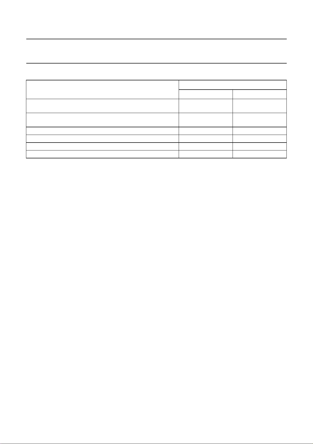
16.5 Suitability of surface mount IC packages for wave and reflow soldering methods
(1)
(3)
, TFBGA,
not suitable suitable
BGA, HTSSON..T
PACKAGE
(3)
, LBGA, LFBGA, SQFP, SSOP..T
VFBGA, XSON
DHVQFN, HBCC, HBGA, HLQFP, HSO, HSOP, HSQFP, HSSON,
not suitable
HTQFP, HTSSOP, HVQFN, HVSON, SMS
(5)
PLCC
, SO, SOJ suitable suitable
LQFP, QFP, TQFP not recommended
SSOP, TSSOP, VSO, VSSOP not recommended
CWQCCN..L
(8)
, PMFP
(9)
, WQCCN..L
(8)
not suitable not suitable
Notes
1. Formore detailed informationon the BGApackagesrefer to the
“(LF)BGAApplication Note”
from your Philips Semiconductors sales office.
2. All surface mount (SMD) packages are moisture sensitive. Depending upon the moisture content, the maximum
temperature (with respect to time) and body size of the package, there is a risk that internal or external package
cracks may occur due to vaporization of the moisture in them (the so called popcorn effect). For details, refer to the
Drypack information in the
“Data Handbook IC26; Integrated Circuit Packages; Section: Packing Methods”
3. These transparent plastic packages are extremely sensitive to reflow soldering conditions and must on no account
be processed through morethan one soldering cycle or subjected toinfrared reflow soldering with peaktemperature
exceeding 217 °C ± 10 °C measured in the atmosphere of the reflow oven. The package body peak temperature
must be kept as low as possible.
4. These packages are not suitable for wave soldering. On versions with the heatsink on the bottom side, the solder
cannot penetrate between the printed-circuit board and the heatsink. On versions with the heatsink on the top side,
the solder might be deposited on the heatsink surface.
5. If wave soldering is considered, then the package must be placed at a 45° angle to the solder wave direction.
The package footprint must incorporate solder thieves downstream and at the side corners.
6. Wave soldering is suitablefor LQFP, QFP and TQFPpackages with a pitch (e) larger than0.8 mm; it is definitely not
suitable for packages with a pitch (e) equal to or smaller than 0.65 mm.
7. Wave soldering is suitable for SSOP, TSSOP, VSO and VSSOP packages with a pitch (e) equal to or larger than
0.65 mm; it is definitely not suitable for packages with a pitch (e) equal to or smaller than 0.5 mm.
8. Image sensor packages in principle should not be soldered. They are mounted in sockets or delivered pre-mounted
on flex foil. However, the image sensor package can be mounted by the client on a flex foil by using a hot bar
soldering process. The appropriate soldering profile can be provided on request.
9. Hot bar soldering or manual soldering is suitable for PMFP packages.
SOLDERING METHOD
WAVE REFLOW
(4)
(5)(6)
(7)
suitable
suitable
suitable
(AN01026);order a copy
(2)
.
2004 Sep 13 34
Page 35

Philips Semiconductors Product specification
Low-power FM stereo radio for
TEA5767HL
handheld applications
17 DATA SHEET STATUS
LEVEL
I Objective data Development This data sheet contains data from the objective specification for product
II Preliminary data Qualification This data sheet contains data from the preliminary specification.
III Product data Production This data sheet contains data from the product specification. Philips
Notes
1. Please consult the most recently issued data sheet before initiating or completing a design.
2. The product status of the device(s) described in this data sheet may have changed since this data sheet was
3. For data sheets describing multiple type numbers, the highest-level product status determinesthe datasheet status.
DATA SHEET
STATUS
published. The latest information is available on the Internet at URL http://www.semiconductors.philips.com.
(1)
PRODUCT
STATUS
(2)(3)
development. Philips Semiconductors reserves the right to change the
specification in any manner without notice.
Supplementary data will be published at a later date. Philips
Semiconductors reserves the right to change the specification without
notice, in order to improve the design and supply the best possible
product.
Semiconductors reserves the right to make changes at any time in order
to improve the design, manufacturing and supply. Relevant changes will
be communicated via a Customer Product/Process Change Notification
(CPCN).
DEFINITION
18 DEFINITIONS Short-form specification The data in a short-form
specification is extracted from a full data sheet with the
same type number and title. For detailed information see
the relevant data sheet or data handbook.
Limiting values definition Limiting values given arein
accordance with the Absolute Maximum Rating System
(IEC 60134). Stress above one or more of the limiting
values may cause permanent damage to the device.
These are stress ratings only and operation of the device
atthese or atanyother conditions abovethosegiven in the
Characteristics sections of the specificationis not implied.
Exposure to limiting values for extended periods may
affect device reliability.
Application information Applications that are
described herein for any of these products are for
illustrative purposes only. Philips Semiconductors make
norepresentationor warranty thatsuchapplicationswill be
suitable for the specified use without further testing or
modification.
19 DISCLAIMERS Life support applications These products are not
designed for use in life support appliances, devices, or
systems where malfunction of these products can
reasonably be expectedto result in personal injury.Philips
Semiconductorscustomersusing or selling theseproducts
for use in such applications do so at their own risk and
agree to fully indemnify Philips Semiconductors for any
damages resulting from such application.
Right to make changes Philips Semiconductors
reserves the right to make changes in the products including circuits, standard cells, and/or software described or contained herein in order to improve design
and/or performance. When the productis infull production
(status ‘Production’), relevant changes will be
communicated via a Customer Product/Process Change
Notification (CPCN). Philips Semiconductors assumes no
responsibility or liability for the use of any of these
products, conveys no licence or title under any patent,
copyright, or mask work right to these products, and
makes no representations or warranties that these
products are free from patent, copyright, or mask work
right infringement, unless otherwise specified.
2004 Sep 13 35
Page 36

Philips Semiconductors – a w orldwide compan y
Contact information
For additional information please visit http://www.semiconductors.philips.com. Fax: +31 40 27 24825
For sales offices addresses send e-mail to: [email protected].
© Koninklijke Philips Electronics N.V. 2004
All rights are reserved. Reproduction in whole or in part is prohibited without the prior written consent of the copyright owner.
The information presented in this document does not form part of any quotation or contract, is believed to be accurate and reliable and may be changed
without notice. No liability will be accepted by the publisher for any consequence of its use. Publication thereof does not convey nor imply any license
under patent- or other industrial or intellectual property rights.
Printed in The Netherlands R30/03/pp36 Date of release:2004 Sep 13 Document order number: 9397 750 13532
SCA76
 Loading...