

Philips TEA1206T-N1 Datasheet

DATA SH EET
Preliminary specification
Supersedes data of 1998 Mar 24
File under Integrated Circuits, IC03
1999 Sep 16
INTEGRATED CIRCUITS
TEA1206T
High efficiency DC/DC converter

1999 Sep 16 2
Philips Semiconductors Preliminary specification
High efficiency DC/DC converter TEA1206T
FEATURES
• Fully integrated DC/DC converter circuit
• Up-or-down conversion
• Start-up from 1.8 V input
• Adjustable output voltage
• High efficiency over large load range
• Power handling capability up to 1 A continuous
average current
• 600 kHz switching frequency
• Low quiescent power consumption
• Synchronizes to external 9 to 20 MHz clock
• True current limit for Li-ion battery compatibility
• Up to 100% duty cycle in down mode
• Undervoltage lockout
• Shut-down function
• 8-pin SO package.
APPLICATIONS
• Cellular and cordless phones, PDAs and others
• Supply voltage source for low-voltage chip sets
• Portable computers
• Battery backup supplies
• Cameras.
GENERAL DESCRIPTION
The TEA1206T (see Fig.1) is a fully integrated DC/DC
converter circuit. Efficient, compact and dynamic power
conversion is achieved using a novel, digitally controlled
Pulse Width and Frequency Modulation (PWFM) like
control concept, integrated low R
dsON
CMOS power
switches with low parasitic capacitances, and fully
synchronous rectification. The device operates at a high
590 kHz switching frequency which enables the use of
minimum size external components. Deadlock is
prevented by an on-chip undervoltage lockout circuit.
Compatibility with Li-ion batteries is guaranteed by an
accurate current limit function.
ORDERING INFORMATION
TYPE NUMBER
PACKAGE
NAME DESCRIPTION VERSION
TEA1206T SO8 plastic small outline package; 8 leads; body width 3.9 mm SOT96-1

1999 Sep 16 3
Philips Semiconductors Preliminary specification
High efficiency DC/DC converter TEA1206T
QUICK REFERENCE DATA
Note
1. Current limit is defined by an external resistor R
lim
, having 1% accuracy. The typical value is presettable between
0.5 and 5.0 A with a spread of ±17.5%.
SYMBOL PARAMETER CONDITIONS MIN. TYP. MAX. UNIT
Voltage levels
V
O(up)
output voltage range in up mode U/D = LOW 2.80 − 5.50 V
V
O(down)
output voltage range in down mode U/D = HIGH 1.25 − 5.50 V
V
i(up)
input voltage range in up mode U/D = LOW V
start
− 5.50 V
V
i(down)
input voltage range in down mode U/D = HIGH 2.80 − 5.50 V
V
start
start-up voltage up mode; IL< 200 mA 1.40 1.60 1.85 V
V
fb
feedback voltage level 1.19 1.24 1.29 V
Current levels
I
q
quiescent current at pin 3 down mode, Vi= 3.6 V 65 75 85 µA
I
shdwn
shut-down current − 210µA
I
limN
current limit NFET up mode; note 1 0.5 − 5.0 A
I
limP
current limit PFET down mode; note 1 0.5 − 5.0 A
I
Lx
maximum continuous current at pin 4 −−1.0 A
Power MOSFETS
R
dsON(N)
pin-to-pin resistance NFET 0.08 0.14 0.20 Ω
R
dsON(P)
pin-to-pin resistance PFET 0.10 0.16 0.25 Ω
Efficiency; see Fig.5
η efficiency V
i
= 3.6 V; L = 10 µH −−−
V
i
= 3.6 up to 4.6 V IL=1mA − 86 − %
I
L
=10mA − 93 − %
I
L
=50mA − 93 − %
I
L
= 100 mA − 93 − %
I
L
= 500 mA − 93 − %
I
L
= 1000 mA; pulsed
load current
− 87 − %
V
i
= 3.6 down to 1.8 V IL=1mA − 83 − %
I
L
=10mA − 90 − %
I
L
=50mA − 91 − %
I
L
= 100 mA − 87 − %
I
L
= 500 mA − 88 − %
I
L
= 1000 mA; pulsed
load current
− 82 − %
Timing
f
sw
switching frequency PWM mode 475 560 645 kHz
f
sync
sync input frequency 9 13 20 MHz
t
res
response time from standby to P
max
− 25 −µs
1999 Sep 16 4
Philips Semiconductors Preliminary specification
High efficiency DC/DC converter TEA1206T
This text is here in white to force landscape pages to be rotated correctly when browsing through the pdf in the Acrobat reader.This text is here in
_white to force landscape pages to be rotated correctly when browsing through the pdf in the Acrobat reader.This text is here inThis text is here in
white to force landscape pages to be rotated correctly when browsing through thepdf in the Acrobat reader.white to force landscape pagesto be ...
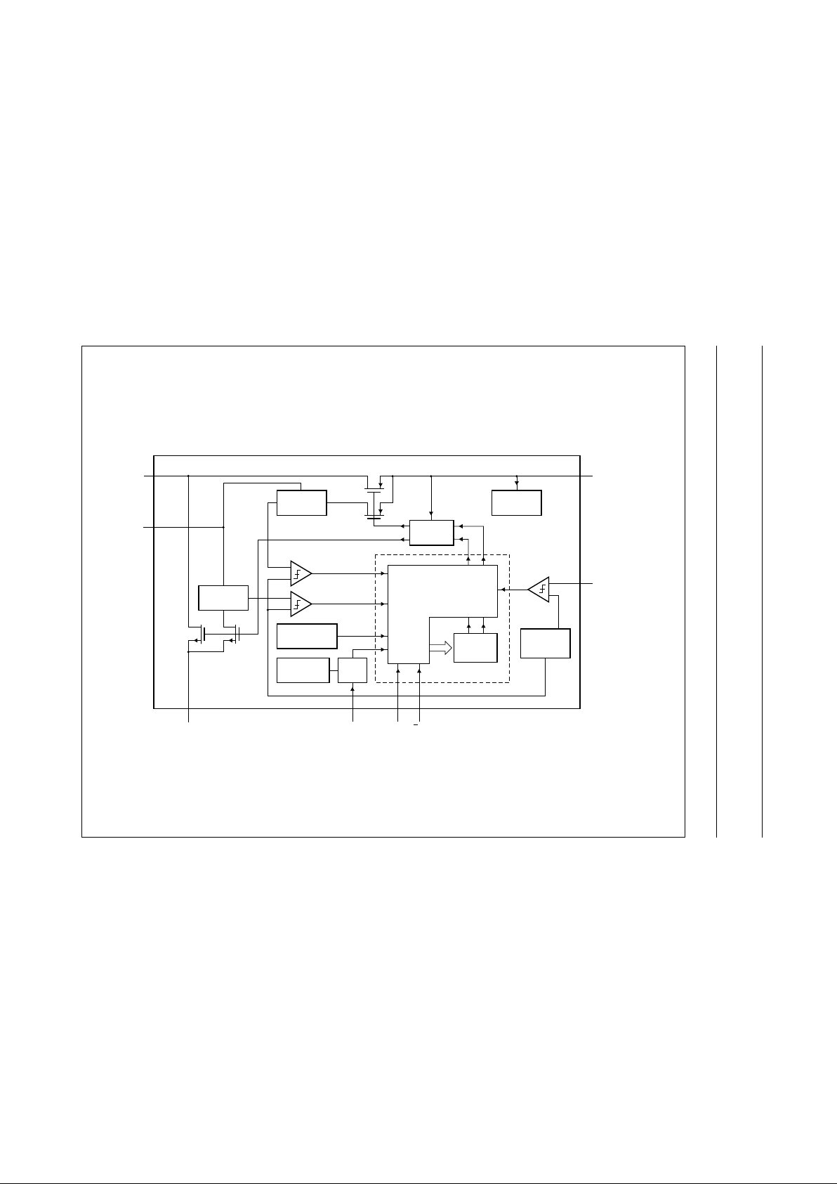
BLOCK DIAGRAM
handbook, full pagewidth
MGM666
CONTROL LOGIC
AND
MODE GEARBOX
START-UP
CIRCUIT
I/V
CONVERTER
I/V
CONVERTER
INTERNAL
SUPPLY
TIME
COUNTER
BAND GAP
REFERENCE
13 MHz
OSCILLATOR
SYNC
GATE
TEMPERATURE
PROTECTION
DIGITAL CONTROLLER
sense FET
P-type POWER FET
sense
FET
SHDN
GND
SYNC U/D
N-type
POWER
FET
LX
UPOUT/DNIN
FB
TEA1206T
5681
4
ILIM
2
3
7
CURRENT LIMIT
COMPARATORS
Fig.1 Block diagram.

1999 Sep 16 5
Philips Semiconductors Preliminary specification
High efficiency DC/DC converter TEA1206T
PINNING
SYMBOL PIN DESCRIPTION
U/D 1 conversion mode selection input
ILIM 2 current limit resistor connection
UPOUT/DNIN 3 up mode; output voltage/
down mode; input voltage
LX 4 inductor connection
SYNC 5 synchronization clock input
GND 6 ground
FB 7 feedback input
SHDWN 8 shut-down input
Fig.2 Pin configuration.
handbook, halfpage
MGM667
1
2
3
4
8
7
6
5
U/D SHDWN
ILIM FB
UPOUT/DNIN GND
LX SYNC
TEA1206T
FUNCTIONAL DESCRIPTION
Control mechanism
TheTEA1206TDC/DCconverterisabletooperateinPFM
(discontinuous conduction) or PWM (continuous
conduction)operation.Allswitching actions are completely
determined by a digital control circuit which uses the
output voltage level as its control input. This novel digital
approach enables the use of a new pulse width and
frequency modulation scheme, which ensures optimum
power efficiency over the complete range of operation of
the converter. The scheme works as follows.
When high output power is requested, the device will
operate in PWM (continuous conduction) mode.
This results in minimum AC currents in the circuit
components and hence optimum efficiency, cost and
EMC. In this mode, the output voltage is allowed to vary
between two predefined voltage levels. As long as the
output voltage stays within this so-called window,
switching continues in a fixed pattern. When the output
voltage reaches one of the window borders, the digital
controller immediately reacts by adjusting the pulse width
and inserting a current step in such a way that the output
voltage stays within the window with higher or lower
current capability. This approach enables very fast
reaction to load variations.
Figure 3 shows the converter’s response to a sudden load
increase. The upper trace shows the output voltage.
The ripple on top of the DC level is a result of the current
in the output capacitor, which changes in sign twice per
cycle, times the capacitor’s internal Equivalent Series
Resistance (ESR). After each ramp-down of the inductor
current, i.e. when the ESR effect increases the output
voltage, the converter determines what to do in the next
cycle. As soon as more load current is taken from the
output the output voltage starts to decay. When the output
voltage becomes lower than the low limit of the window,
a corrective action is taken by a ramp-up of the inductor
current during a much longer time. As a result, the DC
current level is increased and normal PWM control can
continue. The output voltage (including ESR effect) is
again within the predefined window.
Figure 4 depicts the spread of the output voltage window.
Theabsolutevalueismostdependent on spread, while the
actualwindow size is not affected. Forone specific device,
the output voltage will not vary more than 2% typically.
In low output power situations, TEA1206T will switch over
toPFM(discontinuousconduction)mode operation. In this
mode, regulation information from earlier PWM mode
operation is used. This results in optimum inductor peak
current levels in PFM mode, which are slightly larger than
the inductor ripple current in PWM mode. As a result, the
transition between PFM and PWM mode is optimal under
all circumstances. In PFM mode, TEA1206T regulates the
output voltage to the high window limit shown in Fig.3.
Synchronous rectification
For optimal efficiency over the whole load range,
synchronous rectifiers inside TEA1206T ensure that
during the whole second switching phase, all inductor
current will flow through the low-ohmic power MOSFETS.
Special circuitry is included whichdetects that the inductor
current reaches zero. Following this detection, the digital
controller switches off the power MOSFET and proceeds
regulation.
 Loading...