查询TEA1201TS供应商查询TEA1201TS供应商
INTEGRATED CIRCUITS
DATA SH EET
TEA1201TS
0.95 V starting basic power unit
Product specification 2002 Jun 06

Philips Semiconductors Product specification
0.95 V starting basic power unit TEA1201TS
CONTENTS
1 FEATURES
2 APPLICATIONS
3 GENERAL DESCRIPTION
4 ORDERING INFORMATION
5 QUICK REFERENCE DATA
6 BLOCK DIAGRAM
7 PINNING INFORMATION
7.1 Pinning
7.2 Pin description
8 FUNCTIONAL DESCRIPTION
8.1 Control mechanism
8.2 Synchronous rectification
8.3 Start-up
8.4 Undervoltage lockout
8.5 Shut-down
8.6 Power switches
8.7 Temperature protection
8.8 Current limiters
8.9 External synchronization and PWM-only mode
8.10 Behaviour at input voltage exceeding the
specified range
8.11 Control of the additional switch
8.12 Low battery detector
9 LIMITING VALUES
10 THERMAL CHARACTERISTICS
11 QUALITY SPECIFICATION
12 CHARACTERISTICS
13 APPLICATION INFORMATION
13.1 External component selection
14 PACKAGE OUTLINE
15 SOLDERING
15.1 Introduction to soldering surface mount
packages
15.2 Reflow soldering
15.3 Wave soldering
15.4 Manual soldering
15.5 Suitability of surface mount IC packages for
wave and reflow soldering methods
16 DATA SHEET STATUS
17 DEFINITIONS
18 DISCLAIMERS
2002 Jun 06 2

Philips Semiconductors Product specification
0.95 V starting basic power unit TEA1201TS
1 FEATURES
• Complete DC-to-DC converter circuit, one current
switch and a battery low detector
• Configurable for 1, 2 or 3-cell Nickel-Cadmium (NiCd)
or Nickel Metal Hydride (NiMH) batteries and 1 Lithium
Ion (Li-Ion) battery
• Guaranteed DC-to-DC converter start-up from 1-cell
NiCd or NiMH battery, even with a load current
• Upconversion or downconversion
• Internal power MOSFETs featuring a low R
DSon
of
approximately 0.1 Ω
• Synchronous rectification for high efficiency
• Soft start
• PWM-only operating option
• Stand-alone low battery detector requires no additional
supply voltage
• Low battery detection level at 0.90 V, externally
adjustable to a higher level
• Adjustable output voltages
• Shut-down function
• Small outline package
• Advanced 0.6 µm BICMOS process.
2 APPLICATIONS
• Cellular phones
• Cordless phones
• Personal Digital Assistants (PDAs)
• Portable audio players
• Pagers
• Mobile equipment.
3 GENERAL DESCRIPTION
The TEA1201TS is a fully integrated battery power unit
including ahigh-efficiency DC-to-DC converter which runs
from a 1-cell NiCd or NiMH battery, a currentswitch and a
lowbattery detector. Thecircuit can bearrangedin several
ways to optimize the application circuit of a power supply
system. Therefore, the DC-to-DC converter can be
arranged for upconversionor downconversionand the low
battery detector can be configured for several types of
batteries. Accurate low battery detection is possible while
all other blocks are switched off.
The DC-to-DC converter features efficient, compact and
dynamic power conversion using a digital control concept
comparable with Pulse Width Modulation (PWM) and
Pulse Frequency Modulation (PFM), integrated CMOS
power switches with a very low R
DSon
and fully
synchronous rectification.
The device operates at a switching frequency of 600 kHz
which enables the use of external components with
minimum size. The switching frequency can be
synchronized to an external high frequency clock signal.
Optionally, the device can be kept in PWM control mode
only. Deadlock is prevented by an on-chip undervoltage
lockout circuit.
Active current limiting enables efficient conversion in
pulsed-load systems such as Global System for Mobile
communication (GSM) and Digital Enhanced Cordless
Telecommunications (DECT).
The switch canbe usedto controlthe connection of (a part
of) the output load. It shows a low pin-to-pin resistance of
500 mΩ.
The low battery detector has a built-in detection level
which is optimum for a 1-cell NiCd or NiMH battery.
4 ORDERING INFORMATION
TYPE
NUMBER
NAME DESCRIPTION VERSION
PACKAGE
TEA1201TS SSOP16 plastic shrink small outline package; 16 leads; body width 4.4 mm SOT369-1
2002 Jun 06 3

Philips Semiconductors Product specification
0.95 V starting basic power unit TEA1201TS
5 QUICK REFERENCE DATA
SYMBOL PARAMETER CONDITIONS MIN. TYP. MAX. UNIT
DC-to-DC converter
UPCONVERSION
V
I(up)
V
O(up)
V
I(start)
V
O(uvlo)
DOWNCONVERSION
V
I(dwn)
V
O(dwn)
CURRENT LEVELS
I
q(DCDC)
I
shdwn
I
LX(max)
∆I
lim
POWER MOSFETS
R
DSon(N)
R
DSon(P)
EFFICIENCY
η efficiency upconversion VOup to 3.3 V; see Fig.9
TIMING
f
sw
f
i(sync)
t
start
Switch
R
DSon
I
O(max)
General characteristics
V
ref
input voltage V
output voltage V
I(start)
O(uvlo)
− 5.50 V
− 5.50 V
start-up input voltage IL< 10 mA 0.93 0.96 1.00 V
undervoltage lockout voltage 2.0 2.2 2.4 V
input voltage V
O(uvlo)
− 5.50 V
output voltage 1.30 − 5.50 V
quiescent current at pin
− 110 −µA
UPOUT/DNIN
current in shut-down mode V
maximum continuous current at
LBI1=VI(up)
T
=80°C −−1.0 A
amb
= 1.2 V − 65 −µA
pins LX1 and LX2
current limit deviation I
set to 1.0 A
lim
upconversion −12 − +12 %
downconversion −12 − +12 %
drain-to-source on-state
Tj=27°C; IDS= 100 mA − 110 200 mΩ
resistance NFET
drain-to-source on-state
Tj=27°C; IDS= −100 mA − 125 250 mΩ
resistance PFET
V
= 1.2 V; IL= 100 mA − 84 − %
I
V
= 2.4 V; IL=10mA − 92 − %
I
switching frequency PWM mode 480 600 720 kHz
synchronization clock input
6 1320MHz
frequency
start-up time − 10 − ms
drain-to-source resistance in
switched-on state
maximum output current in
V
O(up)=VI(down)
V
< 0.4 V
FB1
V
< 0.4 V −−0.40 A
FB1
=5V;
− 500 750 mΩ
switched-on state
reference voltage 1.165 1.190 1.215 V
2002 Jun 06 4

Philips Semiconductors Product specification
Philips Semiconductors Product specification
0.95 V starting basic power unit TEA1201TS
0.95 V starting basic power unit TEA1201TS
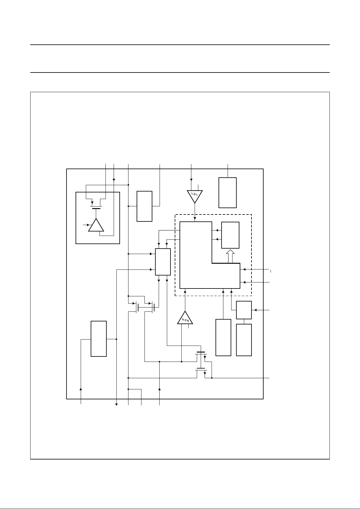
6 BLOCK DIAGRAM
SHDWN0
TEA1201TS
FB1
OUT1
7
6
DETECTOR
LOW BATTERY
UPOUT/DNIN
3, 4
SUPPLY
INTERNAL
P-type
POWER FET
GND
8
CIRCUIT
START-UP
sense FET
FB0
12
ref
V
AND
MODE GEARBOX
CONTROL LOGIC
ref
COMPARATOR
CURRENT LIMIT
V
FET
sense
ref
V
11
VOLTAGE
REFERENCE
TIME
COUNTER
DIGITAL CONTROLLER
GATE
SYNC
13 MHz
PROTECTION
TEMPERATURE
OSCILLATOR
MGW787
SHDWN0
Fig.1 Block diagram.
1413 2 15
SYNC/PWM U/D
This text is here in white to force landscape pages to be rotated correctly when browsing through the pdf in the Acrobat reader.This text is here in
_white to force landscape pages to be rotated correctly when browsing through the pdf in the Acrobat reader.This text is here inThis text is here in
white to force landscape pages tobe rotated correctly when browsing through the pdf in the Acrobat reader. white to force landscape pages to be ...
2002 Jun 06 5
2002 Jun 06 5
9
LBI1
handbook, full pagewidth
10
LBO
GND0
FET
N-type
16
LX2
5
ILIM
1
LX1
POWER

Philips Semiconductors Product specification
0.95 V starting basic power unit TEA1201TS
7 PINNING INFORMATION
7.1 Pinning
handbook, halfpage
SHDWN0
UPOUT/DNIN
UPOUT/DNIN
LX1
ILIM
OUT1
FB1
GND
1
2
3
4
TEA1201TS
5
6
7
8
MGW788
LX2
16
U/D
15
SYNC/PWM
14
GND0
13
FB0
12
V
11
ref
LBO
10
LBI1
9
Fig.2 Pin configuration.
7.2 Pin description
Table 1 SSOP16 package
SYMBOL PIN DESCRIPTION
LX1 1 inductor connection 1
SHDWN0 2 DC-to-DC converter shut-down input
UPOUT/DNIN 3 up mode: DC-to-DC converter output; down mode: DC-to-DC converter input
UPOUT/DNIN 4
ILIM 5 current limiting resistor connection
OUT1 6 switch output
FB1 7 switch control input
GND 8 internal supply ground
LBI1 9 low battery detector input 1
LBO 10 low battery detector output
V
ref
11 reference voltage
FB0 12 DC-to-DC converter feedback input
GND0 13 DC-to-DC converter ground
SYNC/PWM 14 synchronization clock input or PWM-only selection input
U/D 15 conversion mode selection input
LX2 16 inductor connection 2
2002 Jun 06 6

Philips Semiconductors Product specification
0.95 V starting basic power unit TEA1201TS
8 FUNCTIONAL DESCRIPTION
8.1 Control mechanism
The TEA1201TSDC-to-DC converter isable to operatein
PFM (discontinuous conduction) or PWM (continuous
conduction) operating mode. All switching actions are
completely determined by a digital control circuit which
usesthe output voltagelevelas its controlinput.This novel
digital approach enables the use of a new pulse widthand
frequency modulation scheme, which ensures optimum
power efficiency over the complete range of operation of
the converter.
When high output power is requested, the device will
operate in PWM (continuousconduction) operatingmode.
This results in minimum AC currents in the circuit
components and hence optimum efficiency, minimum
costs and low EMC. In this operating mode, the output
voltage isallowed to varybetween two predefined voltage
levels. As long as the output voltage stays within this
so-called window, switching continues in a fixed pattern.
When the output voltage reaches one of the window
borders, the digital controller immediately reacts by
adjusting the pulse width and inserting a current step in
such a waythat theoutput voltagestays within the window
with higher or lower current capability. This approach
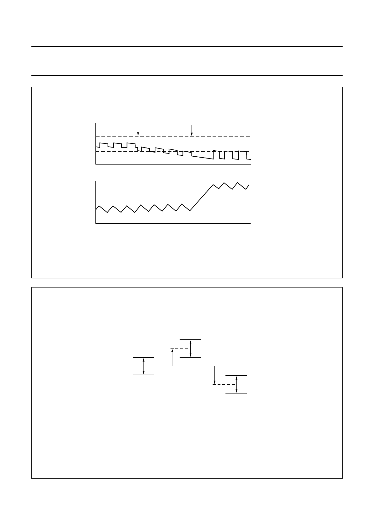
enables very fast reaction to load variations. Figure 3
shows the response of the converter to a sudden load
increase. The upper trace shows the output voltage.
The ripple on top of the DC level is a result of the current
in the output capacitor, which changes in sign twice per
cycle, times the internal Equivalent Series Resistance
(ESR) of the capacitor. After each ramp-down of the
inductor current, i.e. when the ESR effect increases the
output voltage, the converter determines what to do in the
next cycle. As soon as more loadcurrent is taken from the
output the output voltage starts to decay.
Figure 4 shows the spread of the output voltage window.
The absolute value is mostly dependent on spread, while
the actual window size (V
affected. For one specific device, the output voltage will
not vary more than 2% (typical value).
In lowoutput power situations,the TEA1201TS willswitch
over to PFM (discontinuous conduction) operating mode.
In this mode, regulation information from an earlier PWM
operating mode is used. This results in optimum inductor
peak current levels in the PFM mode, which are slightly
larger than the inductor ripple current in the PWM mode.
As a result,the transitionbetween PFMand PWM mode is
optimum under all circumstances. In the PFM mode the
TEA1201TS regulates the output voltage to the high
window limit as shown in Fig.3.
8.2 Synchronous rectification
For optimum efficiency over the whole load range,
synchronous rectifiers inside the TEA1201TS ensure that
during the whole second switching phase, all inductor
current will flow through the low-ohmic power MOSFETs.
Special circuitry is included which detects when the
inductorcurrent reaches zero.Followingthis detection, the
digital controller switches off the power MOSFET and
proceeds with regulation.
8.3 Start-up
Start-up from low input voltage in the boost mode is
realized by anindependent start-uposcillator, which starts
switching the N-type power MOSFET as soon as the
low-battery detector detects a sufficiently high voltage.
The inductor current is limited internally to ensure
soft-starting. The switch actions of the start-up oscillator
will increase the output voltage. As soon as the output
voltage is high enough for normal regulation, the digital
control system takes control over the power MOSFETs.
wdw(high)
− V
wdw(low)
) is not
When theoutput voltage becomes lower than the low limit
of the window, acorrective action is taken bya ramp-upof
theinductor currentduring a muchlonger time. Asa result,
the DC current level is increased and normal PWM control
can continue. The output voltage (including ESR effect) is
again within the predefined window.
2002 Jun 06 7
8.4 Undervoltage lockout
As a result of too high a load or disconnection of the input
power source, the output voltage can drop so low that
normal regulation cannot beguaranteed. In this event, the
device switches back to start-up mode. If the output
voltage drops even further, switching is stopped
completely.

Philips Semiconductors Product specification
0.95 V starting basic power unit TEA1201TS
handbook, full pagewidth
load increase
V
o
I
L
start corrective action
time
time
high window limit
low window limit
MGK925
Fig.3 Response to load increase.
handbook, full pagewidth
V
wdw(high)
V
2%
O
V
wdw(low)
typical
situation
+2%
V
wdw(high)
V
wdw(low)
maximum
positive spread
Fig.4 Output voltage window spread.
2002 Jun 06 8
2%
−2%
V
wdw(high)
2%
V
wdw(low)
maximum
negative spread
MGW789
 Loading...