

Philips TEA1113T-C1, TEA1113-C1 Datasheet
DATA SH EET
Product specification
Supersedes data of 1996 Feb 08
File under Integrated Circuits, IC03
1997 Mar 27
INTEGRATED CIRCUITS
TEA1113
Low voltage versatile telephone
transmission circuit with dialler
interface
1997 Mar 27 2
Philips Semiconductors Product specification
Low voltage versatile telephone
transmission circuit with dialler interface
TEA1113
FEATURES
• Low DC line voltage; operates down to 1.6 V (excluding
polarity guard)
• Voltage regulator with adjustable DC voltage
• Provides a supply for external circuits
• Symmetrical high impedance inputs (64 kΩ) for
dynamic, magnetic or piezo-electric microphones
• Asymmetrical high impedance input (32 kΩ) for electret
microphones
• DTMF input with confidence tone
•
MUTE input for pulse or DTMF dialling
• Receiving amplifier for dynamic, magnetic or
piezo-electric earpieces
• Dynamic limitation in the transmit direction to prevent
distortion of the transmit line and sidetone signals
• AGC line loss compensation for microphone and
earpiece amplifiers
• LED on-hook/off-hook status indication
• Microphone mute function available with switch.
APPLICATION
• Line powered telephone sets, cordless telephones, fax
machines and answering machines.
GENERAL DESCRIPTION
The TEA1113 is a bipolar integrated circuit that performs
all speech and line interface functions required in fully
electronic telephone sets. It performs electronic switching
between speech and dialling. The IC operates at a line
voltage down to 1.6 V DC (with reduced performance) to
facilitate the use of telephone sets connected in parallel.
A current (proportional to the line current and internally
limited to 19.5 mA) is available to drive an LED which
indicates the on-hook/off-hook status.
The transmit signal on the line is dynamically limited to
prevent distortion at high transmit levels for both the
sending line and sidetone signals. The microphone
amplifier can be disabled during speech condition by
means of a microphone mute function.
All statements and values refer to all versions unless
otherwise specified.
QUICK REFERENCE DATA
I
line
= 15 mA; VEE=0V; R
SLPE
=20Ω; C
DLS
= 470 nF; AGC pin connected to VEE; Z
line
= 600 Ω; f = 1 kHz;
T
amb
=25°C; unless otherwise specified.
SYMBOL PARAMETER CONDITIONS MIN. TYP. MAX. UNIT
I
line
line current operating range normal operation 11 − 140 mA
with reduced performance 1 − 11 mA
I
LED(max)
maximum supply current available I
line
=18 mA − 0.6 − mA
I
line
>76mA − 19.5 − mA
V
LN
DC line voltage 3.7 4.0 4.3 V
V
LN(max)(p-p)
maximum output voltage swing
(peak-to-peak value)
3.8 4.65 − V
I
CC
internal current consumption VCC= 3.2 V − 1.3 1.6 mA
V
CC
supply voltage for peripherals Ip= 0 mA 2.8 3.2 − V
G
vtrx
typical voltage gain range
microphone amplifier V
MIC
= 2 mV (RMS) 38.8 − 51.8 dB
receiving amplifier V
IR
= 4 mV (RMS) 19.3 − 31.3 dB
∆G
vtrx
gain control range for microphone and
receiving amplifiers with respect to
I
line
=15mA
I
line
=85mA − 5.8 − dB
∆G
vtxm
microphone amplifier gain reduction − 80 − dB
1997 Mar 27 3
Philips Semiconductors Product specification
Low voltage versatile telephone
transmission circuit with dialler interface
TEA1113
ORDERING INFORMATION
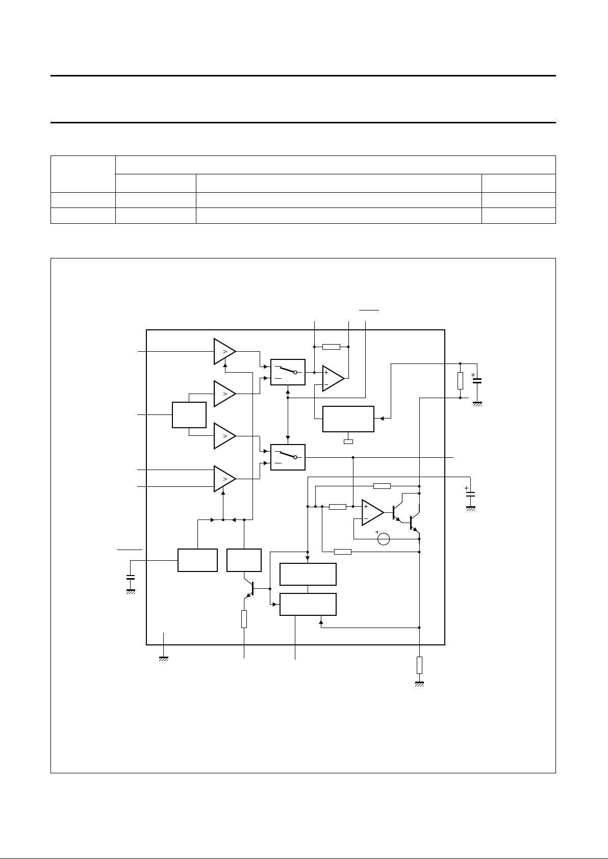
BLOCK DIAGRAM
TYPE
NUMBER
PACKAGE
NAME DESCRIPTION VERSION
TEA1113 DIP16
plastic dual in-line package; 16 leads (300 mil)
SOT38-4
TEA1113T SO16
plastic small outline package; 16 leads; body width 3.9 mm
SOT109-1
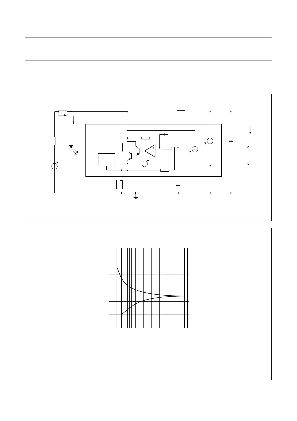
Fig.1 Block diagram.
handbook, full pagewidth
ATT.
DTMF
V− I
DYNAMIC
LIMITER
AGC
CIRCUIT
CURRENT
REFERENCE
LOW VOLTAGE
CIRCUIT
LED
DRIVER
IR
MIC+
MIC−
DLS/MMUTE
V
EE
I
LED
AGC
SLPE
TEA1113
5
4
231013
11
6
12
15 14 8
16
1
7
9
GAS
GAR
QR
LN
V
CC
REG
MUTE
V− I
V− I
V− I
MBG018
1997 Mar 27 4
Philips Semiconductors Product specification
Low voltage versatile telephone
transmission circuit with dialler interface
TEA1113
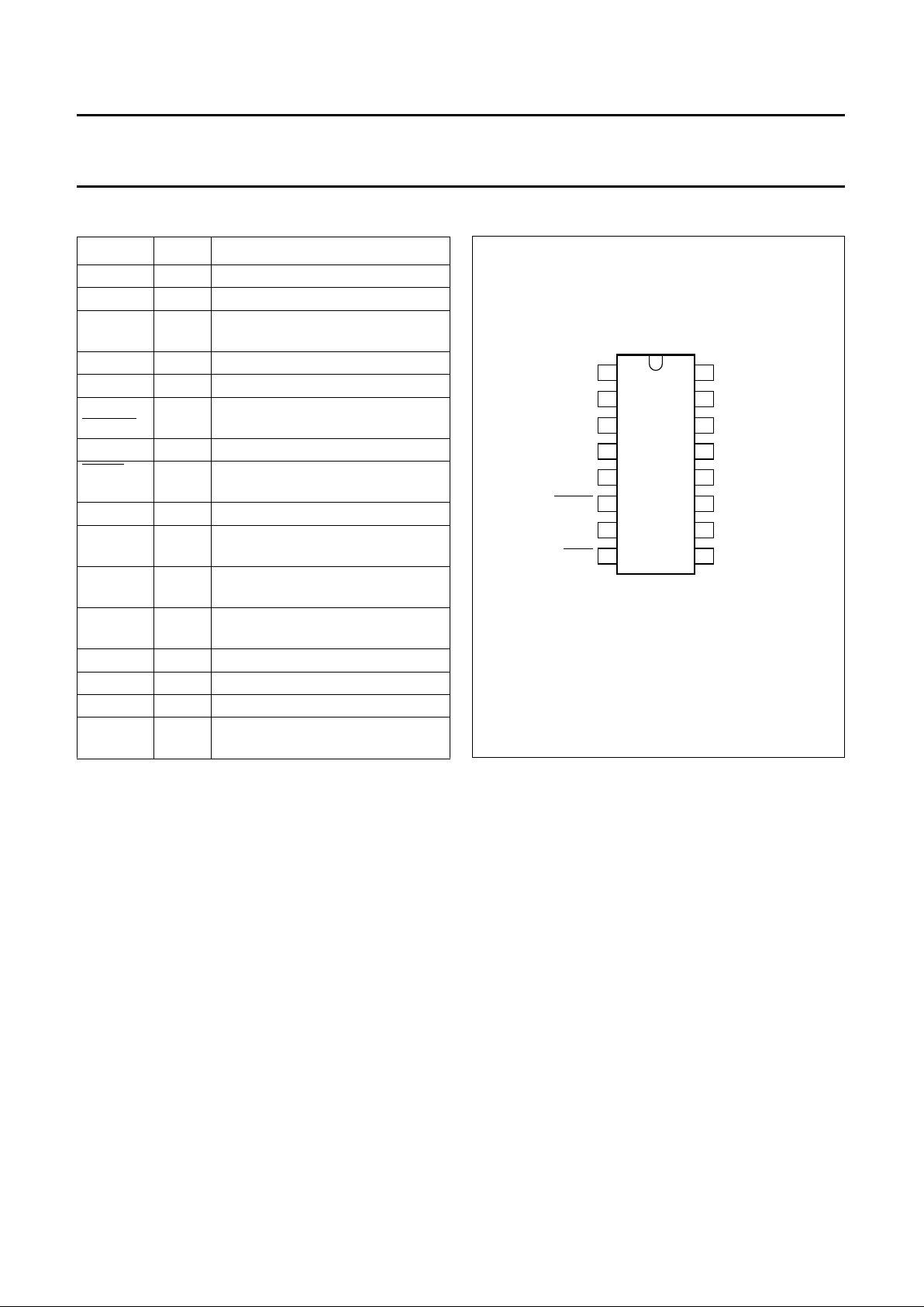
PINNING
SYMBOL PIN DESCRIPTION
LN 1 positive line terminal
SLPE 2 slope (DC resistance) adjustment
I
LED
3 available output current to drive an
LED
REG 4 line voltage regulator decoupling
GAS 5 sending gain adjustment
DLS/
MMUTE
6 dynamic limiter timing adjustment
and microphone mute input
DTMF 7 dual-tone multi-frequency input
MUTE 8 mute input to select speech or
dialling mode (active LOW)
IR 9 receiving amplifier input
AGC 10 automatic gain control - line loss
compensation
MIC− 11 inverting microphone amplifier
input
MIC+ 12 non-inverting microphone amplifier
input
V
EE
13 negative line terminal
QR 14 receiving amplifier output
GAR 15 receive gain adjustment
V
CC
16 supply voltage for speech circuit
and peripherals
Fig.2 Pin configuration.
handbook, halfpage
TEA1113
MBG015
1
2
3
4
5
6
7
8
16
15
14
13
12
11
10
9
V
CC
GAR
QR
V
EE
MIC+
MIC−
AGC
IR
LN
SLPE
I
LED
REG
GAS
DLS/MMUTE
DTMF
MUTE
FUNCTIONAL DESCRIPTION
All data given in this chapter are typical values, except
when otherwise specified.
Supply (pins LN, SLPE, V
CC
and REG)
The supply for the TEA1113 and its peripherals is obtained
from the telephone line.
The ICs generate a stabilized reference voltage (V
ref
)
between pins LN and SLPE. This reference voltage is
equal to 3.7 V, is temperature compensated and can be
adjusted by means of an external resistor (RVA). It can be
increased by connecting the RVA resistor between
pins REG and SLPE, or decreased by connecting the R
VA
resistor between pins REG and LN. The voltage at
pin REG is used by the internal regulator to generate the
stabilized reference voltage and is decoupled by a
capacitor (C
REG
) which is connected to VEE. This
capacitor, converted into an equivalent inductance (see
Section “Set impedance”), realizes the set impedance
conversion from its DC value (R
SLPE
) to its AC value
(R
CC
in the audio-frequency range). The voltage at pin
SLPE is proportional to the line current. Figure 3 illustrates
the supply configuration.
The IC regulates the line voltage at the pin LN, and it can
be calculated as follows:
I
line
: line current
ICC: current consumption of the IC
Ip: supply current for peripheral circuits
I*: current consumed between LN and V
EE
I
LED
: supply current for the LED component
Ish: the excess line current shunted to SLPE (and VEE)
via LN.
V
LN
V
refRSLPEISLPE
×+=
I
SLPEIlineICC
– Ip– I∗– I
LED
I+
sh
==
1997 Mar 27 5
Philips Semiconductors Product specification
Low voltage versatile telephone
transmission circuit with dialler interface
TEA1113
The preferred value for R
SLPE
is 20 Ω. Changing R
SLPE
will affect more than the DC characteristics; it also influences the
microphone and DTMF gains, the LED supply current characteristic, the gain control characteristics, the sidetone level
and the maximum output swing on the line.
Fig.3 Supply configuration.
handbook, full pagewidth
LED
DRIVER
I
sh
I
SLPE
REG
LN
SLPE
V
EE
V
CC
R
CC
C
VCC
I
CC
C
REG
R
SLPE
V
exch
R
exch
I
LED
I
LED
I
line
R
line
TEA1113
I
*
I
p
peripheral
circuits
100 µF
4.7 µF
20 Ω
619 Ω
MBG019
from preamp
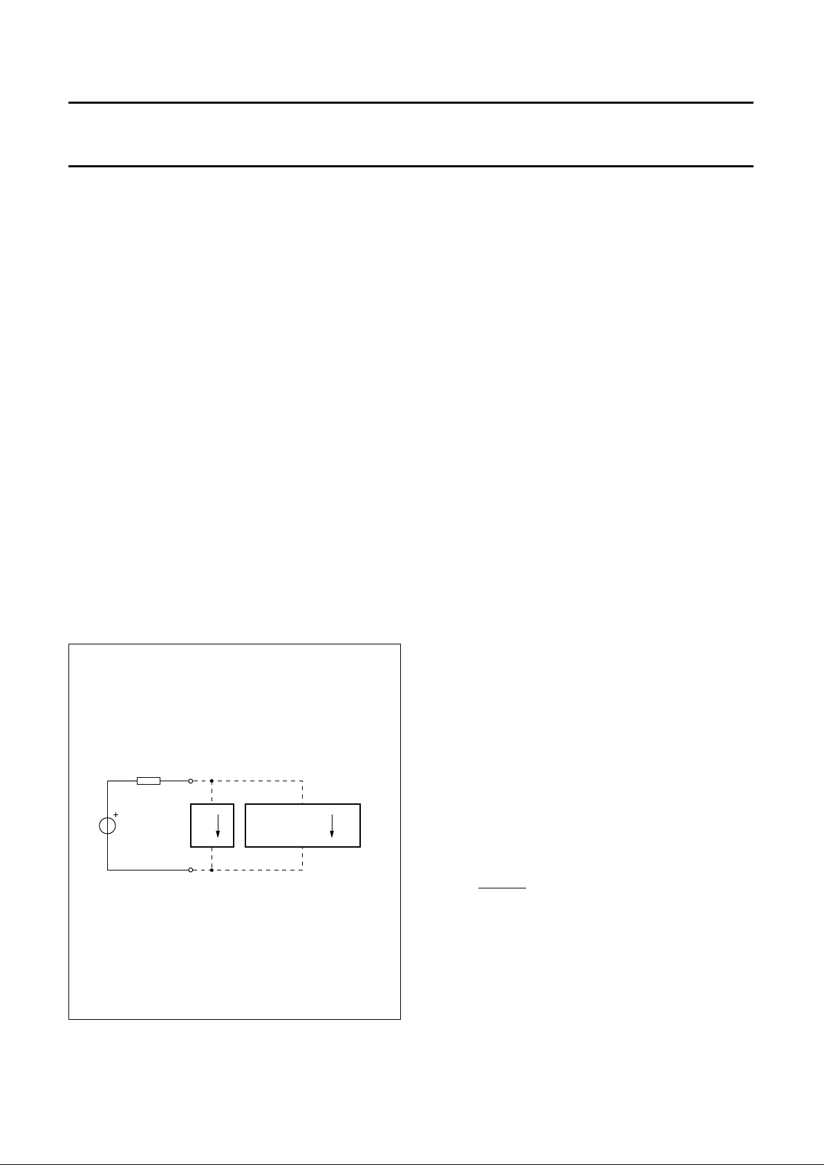
Fig.4 Reference voltage adjustment by a RVA resistor.
(1) RVA between REG and SLPE.
(2) No RVA.
(3) RVA between REG and LN.
handbook, halfpage
5.5
V
ref
(V)
2.5
3.5
4.5
RVA (Ω)
10
4
MGD188
10
5
10
6
10
7
(1)
(2)
(3)
1997 Mar 27 6
Philips Semiconductors Product specification
Low voltage versatile telephone
transmission circuit with dialler interface
TEA1113
The internal circuitry of the TEA1113 is supplied from
pin VCC. This voltage supply is derived from the line
voltage by means of a resistor (RCC) and must be
decoupled by a capacitor C
VCC
. It may also be used to
supply peripheral circuits such as dialling or control
circuits. The VCC voltage depends on the current
consumed by the IC and the peripheral circuits as shown
by the formula (see also Figs 5 and 6). R
CCint
is the internal
impedance of the voltage supply point, and I
rec
is the
current consumed by the output stage of the earpiece
amplifier.
The DC line current flowing into the set is determined by
the exchange supply voltage (V
exch
), the feeding bridge
resistance (R
exch
), the DC resistance of the telephone line
(R
line
) and the reference voltage (V
ref
). With line currents
below 8 mA, the internal reference voltage (generating
V
ref
) is automatically adjusted to a lower value. This means
that more sets can operate in parallel with DC line voltages
(excluding the polarity guard) down to an absolute
minimum voltage of 1.6 V. At currents below 8 mA, the
circuit has limited sending and receiving levels. This is
called the low voltage area.
V
CC
V
CCORCCintIpIrec
–()×–=
V
CCO
VLNR
CCICC
×–=
handbook, halfpage
PERIPHERAL
CIRCUIT
I
P
I
rec
R
CCintVCC
V
EE
V
CCO
MBE792
Fig.5 VCC voltage supply for peripherals.
Set impedance
In the audio frequency range, the dynamic impedance is
mainly determined by the RCC resistor. The equivalent
impedance of the circuits is illustrated in Fig.7.
LED supply (pin I
LED
)
The TEA1113 gives an on-hook/off-hook status indication.
This is achieved by a current made available to drive an
LED connected between pins I
LED
and LN. In the low
voltage area, which corresponds to low line current
conditions, no current is available for this LED. For line
currents higher than a threshold current, the I
LED
current
increases proportionally to the line current (with a ratio of
one third).The I
LED
current is internally limited to 19.5 mA
(see Fig.8).
For 17 mA < I
line
< 77 mA:
This LED driver is referenced to SLPE. Consequently, all
the I
LED
supply current will flow through the R
SLPE
resistor.
The AGC characteristics are not disturbed (see Fig.3 for
the supply configuration).
Microphone amplifier (pins MIC+, MIC− and GAS)
The TEA1113 has symmetrical microphone inputs.
The input impedance between pins MIC+ and MIC− is
64 kΩ (2 × 32 kΩ). The voltage gain from pins MIC+/MIC−
to pin LN is set to 51.8 dB (typ). The gain can be
decreased by connecting an external resistor R
GAS
between pins GAS and REG. The adjustment range is
13 dB. A capacitor C
GAS
connected between pins GAS
and REG can be used to provide a first-order low-pass
filter. The cut-off frequency corresponds to the time
constant C
GAS
× (R
GASint
// R
GAS
). R
GASint
is the internal
resistor which sets the gain with a typical value of 69 kΩ.
Automatic gain control is provided on this amplifier for line
loss compensation.
Dynamic limiter and microphone mute
(pin DLS/
MMUTE)
The dynamic limiter only acts on the microphone channel,
this is to prevent clipping of the line signal. To prevent
distortion, the microphone gain is rapidly reduced when
peaks on the line signal exceed an internally determined
threshold level or when the current in the transmit output
stage is insufficient. The time in which the gain reduction
is realized is very short (attack time). The microphone
channel stays in the reduced gain condition until the peaks
I
LED
I
line
17–
3
----------------------
=
 Loading...