

Philips TEA1111A User Manual
查询TEA1111A供应商
INTEGRATED CIRCUITS
DATA SH EET
TEA1111A
Speech circuit with dialler interface,
regulated supply and earpiece
volume control
Product specification
Supersedes data of 1999 Sep 28
File under Integrated Circuits, IC03
1999 Nov 22

Philips Semiconductors Product specification
Speech circuit with dialler interface, regulated
supply and earpiece volume control
FEATURES
• Low DC linevoltage; operates down to 1.5 V (excluding
voltage drop across external polarity guard)
• Line voltage regulator with adjustable DC voltage
• 3.25 V regulated strong supply point for peripheral
circuits compatible with:
– Speech mode
– Ringer mode
– Trickle mode.
• Transmit stage with:
– Microphone amplifier with symmetrical high
impedance inputs
– DTMF amplifier with confidence tone on earpiece.
• Receive stage with:
– Earpiece amplifier with adjustable gain and volume
control.
• MUTE input for pulse or DTMF dialling
• AGC line loss compensation for microphone and
earpiece
• LED control output.
APPLICATIONS
• Line powered telephone sets with LCD module
• Cordless telephones
• Fax machines
• Answering machines.
GENERAL DESCRIPTION
The TEA1111A is a bipolar integrated circuit that performs
all speech and line interface functions required in fully
electronic telephone sets. It performs electronic switching
between speech and dialling. The IC operates at a line
voltage down to 1.5 V DC (with reduced performance) to
facilitate the use of telephone sets connected in parallel.
When the line current is high enough, a fixed amount of
current is derived from the LN pin in order to create a
strong supply point at pin VDD. The voltage at pin VDD is
regulated to 3.25 V to supply peripherals such as dialler,
LCD module and microcontroller.
TEA1111A
QUICK REFERENCE DATA
I
= 15 mA; VEE=0V; V
line
according to test circuits given in Figs 14, 15 and 16; T
VCI
=0V; R
=20Ω; AGC pin connected to VEE; Z
SLPE
=25°C; unless otherwise specified.
amb
= 600 Ω; f = 1 kHz; measured
line
SYMBOL PARAMETER CONDITIONS MIN. TYP. MAX. UNIT
I
line
line current operating range normal operation 11 − 140 mA
with reduced
1 − 11 mA
performance
V
LN
I
CC
V
CC
V
DD
I
DD
G
v(TX)
G
v(QR)
∆G
v(QR)
∆G
v(trx)
∆G
v(trx)(m)
DC line voltage 3.7 4.0 4.3 V
internal current consumption VCC= 3.3 V − 1.15 1.4 mA
supply voltage for internal circuitry (unregulated) IP=0mA − 3.3 − V
regulated supply voltage for peripherals
speech mode I
ringer mode I
= −3 mA 2.95 3.25 3.55 V
DD
= 75 mA 3.0 3.3 3.6 V
DD
available supply current for peripherals −−−3mA
typical voltage gain for microphone amplifier V
= 4 mV (RMS) 43.2 44.2 45.2 dB
MIC
typical voltage gain for earpiece amplifier VIR= 4 mV (RMS) 26.4 27.4 28.4 dB
volume control range for earpiece amplifier 0 14.5 − dB
gain control range for microphone and earpiece
amplifiers with respect to I
=15mA
line
gain reduction for microphone and earpiece
I
=85mA − 6.0 − dB
line
MUTE = LOW − 80 − dB
amplifiers
1999 Nov 22 2
Philips Semiconductors Product specification
Speech circuit withdialler interface,regulated
TEA1111A
supply and earpiece volume control
ORDERING INFORMATION
TYPE
NUMBER
NAME DESCRIPTION VERSION
TEA1111AT SO16 plastic small outline package; 16 leads; body width 3.9 mm SOT109-1
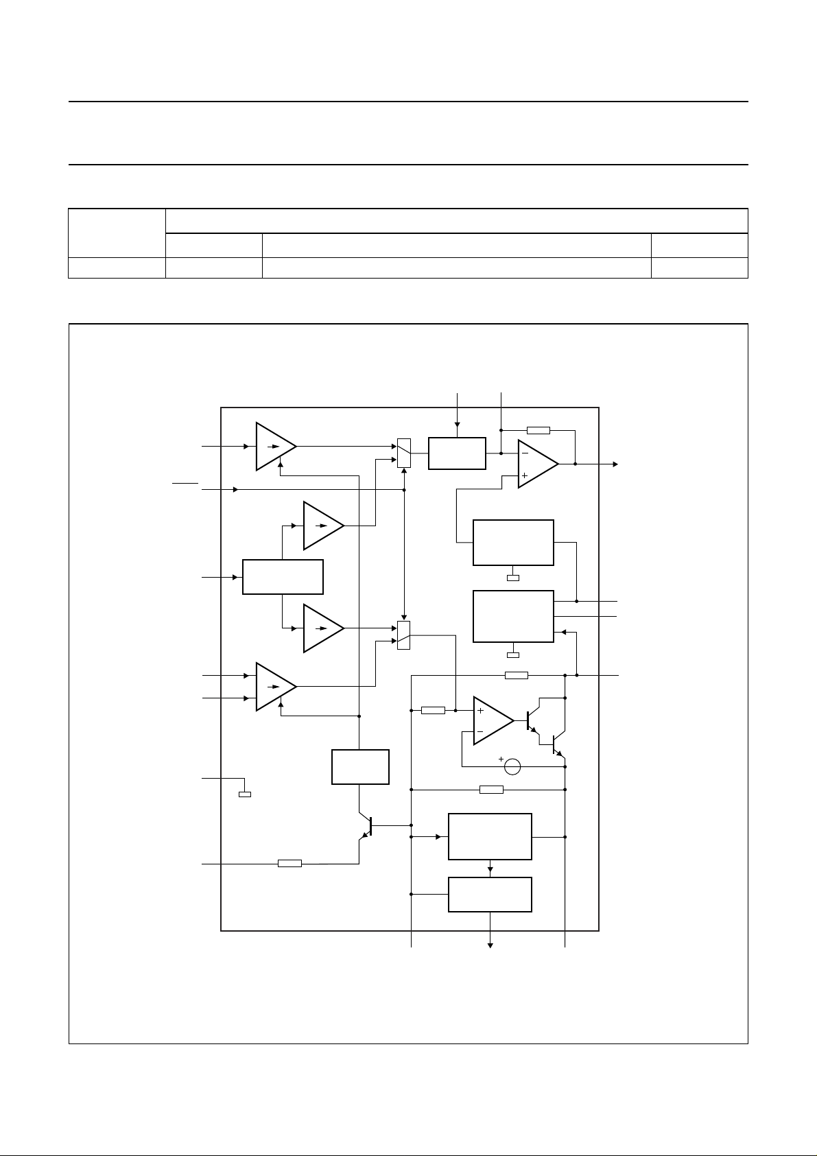
BLOCK DIAGRAM
handbook, full pagewidth
receive
amplifier
VI
MUTE
4
IR
8
PACKAGE
VOLUME
CONTROL
GARVCI
129
earpiece
amplifier
11
QR
DTMF
MIC+
MIC−
V
EE
AGC
6
ATTENUATOR
13
14
microphone
amplifier
10
5
VI
VI
VI
TEA1111A
AGC
CIRCUIT
0.5V
CC
CURRENT AND
VOLTAGE
REFERENCE
V
DD
REGULATOR
LOW VOLTAGE
CIRCUIT
LED CONTROL
153
16
V
CC
7
V
DD
1
LN
2
FCA051
Fig.1 Block diagram.
1999 Nov 22 3
SLPELEDCREG
Philips Semiconductors Product specification
Speech circuit withdialler interface,regulated
supply and earpiece volume control
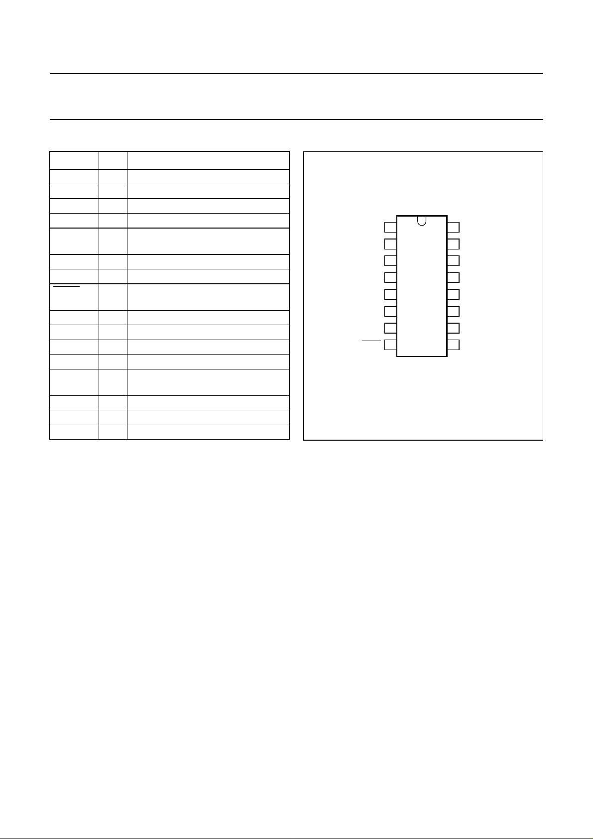
PINNING
SYMBOL PIN DESCRIPTION
LN 1 positive line terminal
SLPE 2 slope (DC resistance) adjustment
REG 3 line voltage regulator decoupling
IR 4 receive amplifier input
AGC 5 automatic gain control/
line loss compensation
DTMF 6 dual-tone multi-frequency input
V
DD
7 regulated supply for peripherals
MUTE 8 mute input to select speech or
dialling mode (active LOW)
VCI 9 volume control input
V
EE
10 negative line terminal
QR 11 earpiece amplifier output
GAR 12 earpiece amplifier gain adjustment
MIC+ 13 non-inverting microphone amplifier
input
MIC− 14 inverting microphone amplifier input
LEDC 15 LED control output
V
CC
16 supply voltage for internal circuit
handbook, halfpage
LN
1
SLPE
2
3
REG
IR
4
TEA1111A
5
AGC
DTMF
6
V
7
DD
8
MUTE
FCA052
Fig.2 Pin configuration.
TEA1111A
V
16
CC
LEDC
15
14
MIC−
13
MIC+
12
GAR
11
QR
V
10
EE
VCI
9
FUNCTIONAL DESCRIPTION
All data given in this chapter concerns typical values,
except when otherwise specified.
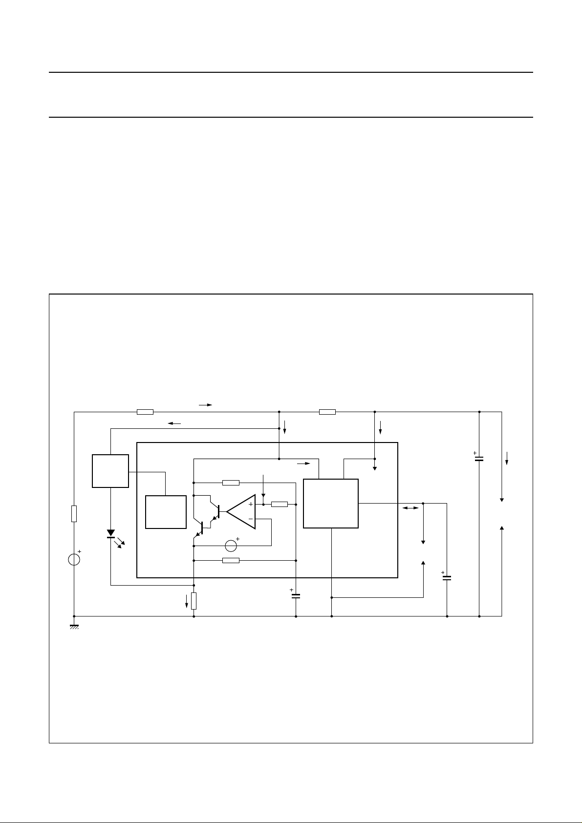
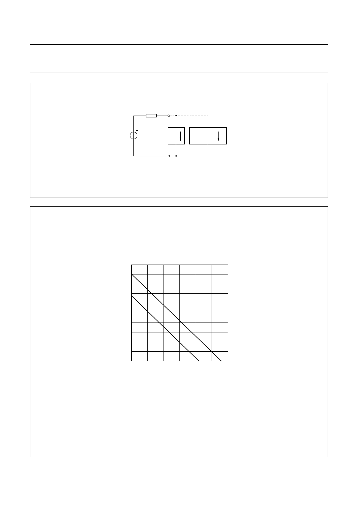
Supply (pins LN, SLPE, REG, VCCand VDD)
The supply for the TEA1111A and its peripherals is
obtained from the telephone line (see Fig.3).
HE LINE INTERFACE (PINS LN, SLPE AND REG)
T
The IC generates a stabilized reference voltage (V
across pins LN and SLPE. V
is temperature
ref
ref
)
compensated and can be adjusted by using an external
resistor (RVA). V
equals 3.8 V and can be increased by
ref
connecting RVA between pins REG and SLPE or
decreased by connecting R
between pins REG and LN.
VA
The voltage at pin REG is used by the internal regulator to
generate V
and is decoupled by C
ref
, which is
REG
connected to VEE. This capacitor, converted to an
equivalent inductance, (see Section “Set impedance”)
determines the set impedance conversion from its DC
value (R
) to its AC value (RCCin the audio-frequency
SLPE
range). The voltage at pin SLPE is proportional to the line
current.
The voltage at pin LN is:
V
LN=Vref+RSLPE
I
SLPE=Iline
− ICC− IP− I
× I
SLPE
SUP
− I
LEDC
where:
I
= line current
line
ICC= current consumption of the IC
IP= supply current for external circuits
I
= current consumed between LN and VEE by the
SUP
VDD regulator
I
= supply current for external LED circuitry.
LEDC
Thepreferredvaluefor R
is 20 Ω.ChangingR
SLPE
SLPE
will
affect more than the DC characteristics; it also influences
the microphone and DTMF gains, the gain control
characteristics, the sidetone level and the maximum
output swing on the line.
The DC line current flowing into the set is determined by
the exchange supply voltage (V
resistance (R
line (R
) and the reference voltage (V
line
currents below I
(generatingV
), the DC resistance of the telephone
EXCH
(9 mA), the internal reference voltage
low
)isautomaticallyadjusted to a lower value.
ref
), the feeding bridge
EXCH
). With line
ref
1999 Nov 22 4
Philips Semiconductors Product specification
Speech circuit withdialler interface,regulated
supply and earpiece volume control
This means that several sets can operate in parallel with
DC line voltages (excluding the polarity guard) down to an
absolute minimum voltage of 1.5 V. At line currents below
I
, the circuit has limited sending and receiving levels.
low
This is called the low voltage area.
THE INTERNAL SUPPLY POINT (PIN VCC)
The internal circuitry of the TEA1111A is supplied from
pin V
. This voltage supply is derived from the line
CC
voltage by means of a resistor (RCC) and must be
decoupled by a capacitor C
. It may also be used to
VCC
supply some external circuits.
The V
current consumed by the IC and the peripheral circuits as:
V
CC0=VLN
VCC=V
Where I
the earpiece amplifier.
TEA1111A
voltage (see also Figs 4 and 5) depends on the
CC
− RCC× I
− RCC× (IP+I
CC0
is the current consumed by the output stage of
rec
CC
rec
)
handbook, full pagewidth
LED
CIRCUIT
R
EXCH
V
EXCH
R
line
LEDC
CONTROL
LED
I
SLPE
I
LEDC
R
20 Ω
SLPE
I
line
from preamplifier
I
LN
LN
I
SUP
REGSLPE
C
4.7 µF
R
CC
V
DD
REGULATOR
V
REG
internal
circuitry
TEA1111A
EE
I
CC
V
V
CC
DD
I
DD
peripherals
C
VCC
100 µF
C
VDD
220 µF
external
circuits
FCA053
I
P
Fig.3 Supply configuration.
1999 Nov 22 5
Philips Semiconductors Product specification
Speech circuit with dialler interface, regulated
supply and earpiece volume control
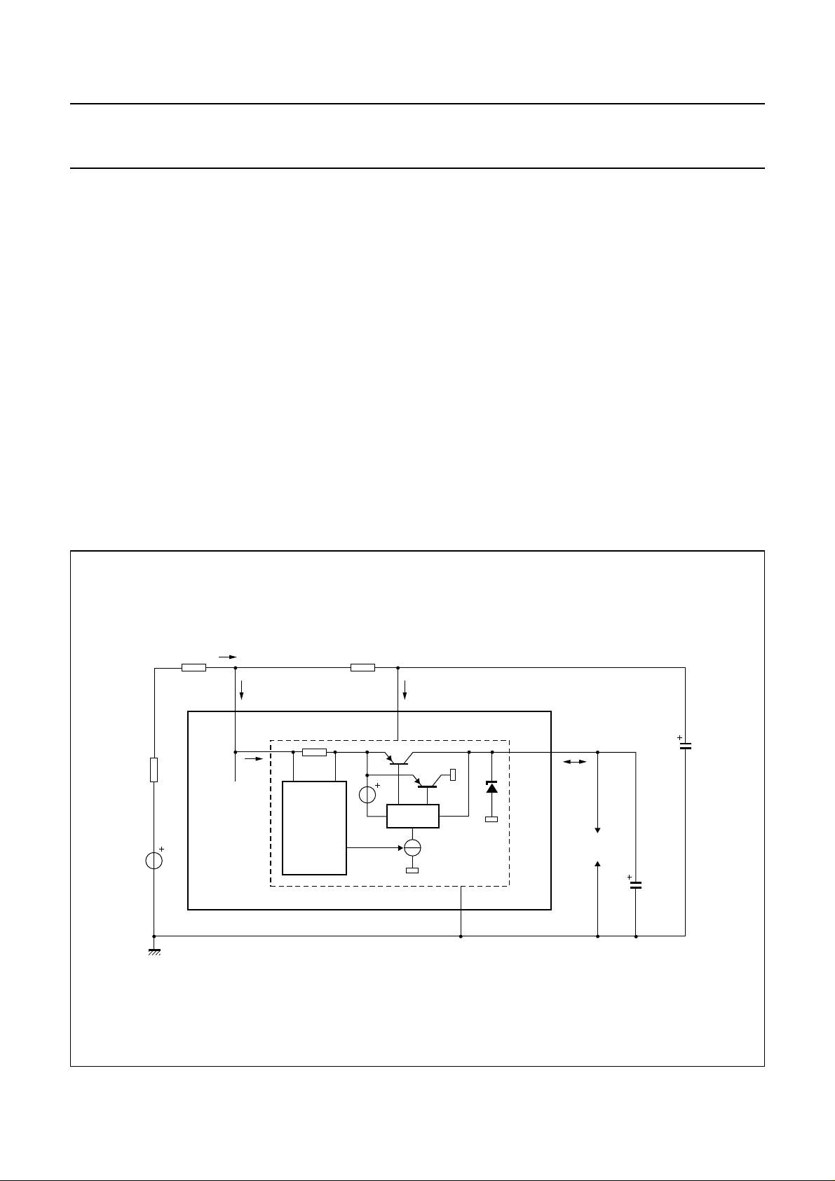
V
R
CC0
handbook, halfpage
Fig.4 VCC used as supply voltage for external circuits.
CC
V
CC
I
rec
V
EE
EXTERNAL
CIRCUITS
I
P
MGK806
TEA1111A
handbook, halfpage
VCC≥ 2.2 V; VLN= 4 V at I
(1) Curve 1 is valid when the earpiece amplifier is driven: V
(2) Curve 2 is valid when the earpiece amplifier is not loaded.
= 15 mA; RCC= 619 Ω; R
line
2
I
P
(mA)
1.6
1.2
0.8
0.4
0
2.2 2.6 3.4
SLPE
(1) (2)
=20Ω.
= 150 mV; RL= 150 Ω.
QR(rms)
3.0
FCA054
VCC (V)
Fig.5 Typical current IP available from VCC for peripheral circuitry.
1999 Nov 22 6
Philips Semiconductors Product specification
Speech circuit with dialler interface, regulated
supply and earpiece volume control
THE REGULATED SUPPLY POINT (PIN VDD)
The V
regulator delivers a stabilized voltage for the
DD
peripherals in transmission mode (nominal VLN) as well as
in ringer mode (VLN= 0 V). The regulator (see Fig.6)
consists of a sense input circuit fed by pin LN, a current
switch and a V
output stabilizer.
DD
Theregulatorfunctiondependsonthetransmission,ringer
and trickle modes as follows:
• Transmissionmode:Theregulatoroperatesasacurrent
source at the LN input; it takes a constant current of
= 4.3 mA (at nominal conditions) from pin LN.
I
SUP
The current switch reduces the distortion on the line at
large signal swings. Output V
follows the DC voltage
DD
at pin LN (with typically 0.35 V difference) up to
VDD= 3.25 V. The input current of the regulator is
constant while the output (source) current is determined
by the consumption of the peripherals. The difference
between input and output currents is shunted by the
internal VDD stabilizer.
• Ringer mode: The regulator operates as a shunt
• Trickle mode: When VDD is below 2 V, the regulator is
TEA1111A
stabilizer to keep V
VLNequals 0 V while the input current into pin VDD is
delivered by the ringingsignal. VDDhas to be decoupled
by a capacitor C
inhibited. The current consumption of the VDDregulator
in trickle mode is very low to save most of the trickle
current for memory retention of a dialler.
at 3.3 V. The input voltage
DD
.
VDD
handbook, full pagewidth
R
EXCH
V
EXCH
R
line
TEA1111A
I
line
LN
I
SUP
R
CC
I
LN
SENSE
I
CC
V
CC
SWITCH
VDD regulator
V
EE
C
V
DD
I
DD
peripherals
C
VDD
220 µF
FCA055
VCC
100 µF
Fig.6 VDD regulator configuration.
1999 Nov 22 7
Philips Semiconductors Product specification
Speech circuit with dialler interface, regulated
supply and earpiece volume control
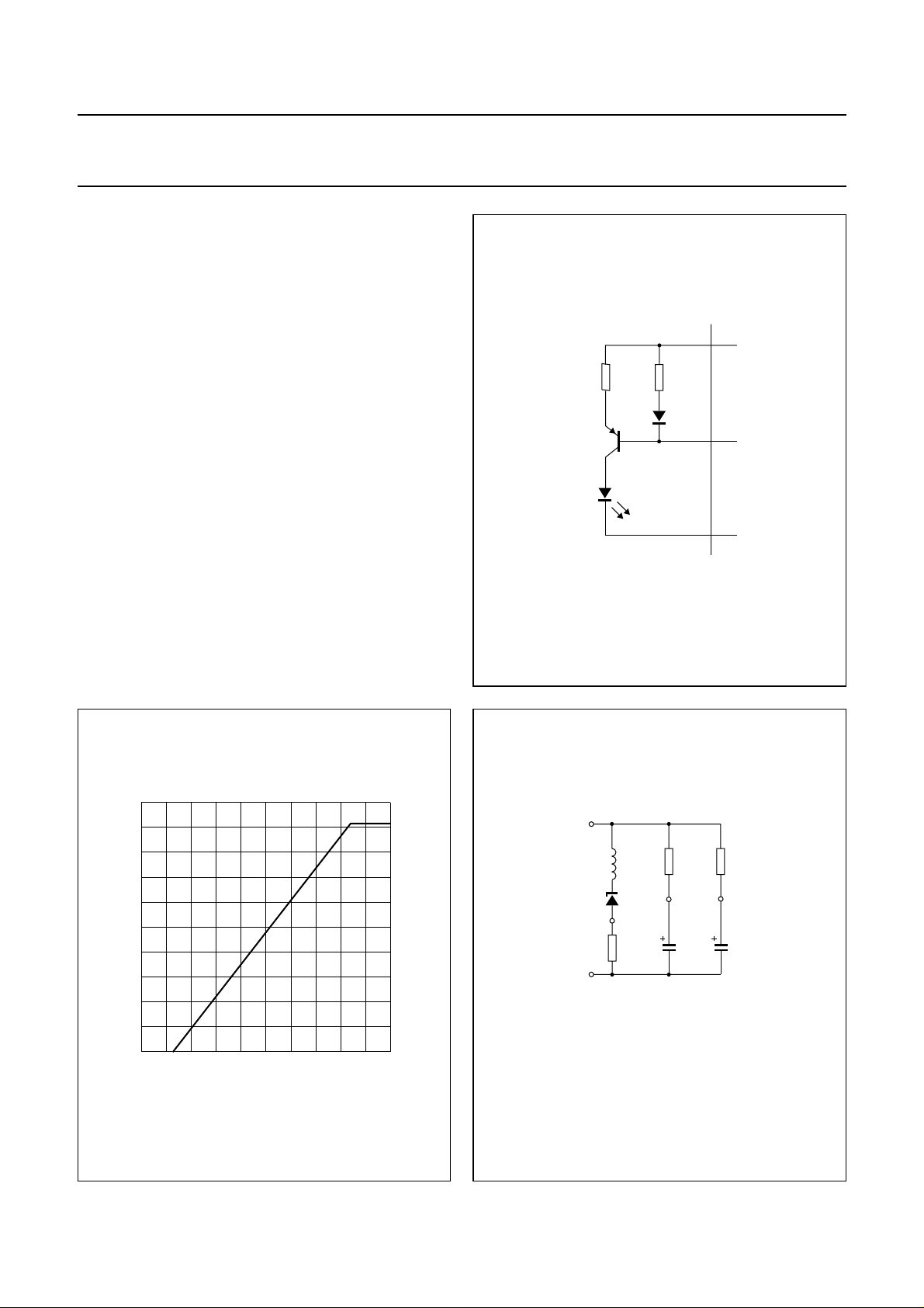
LED control (pin LEDC)
The TEA1111A gives an on-hook/off-hook status
indication. This is achieved by a current made available at
pin LEDC to drive an external LED circuit connected
between pins SLPE and LN (see Fig.7). In the low voltage
area, which corresponds to low line current conditions, no
current is available for this LED. For line currents higher
than a threshold, the LEDC current increases
proportionally to the line current (with a ratio of 1:150).
The LEDC current is internally limited to 470 µA
(see Fig.8).
I
12–
For 12 mA < I
< 82 mA:
line
I
LEDC
This LED circuit is referenced to SLPE. Consequently, all
theLEDsupply current will flow through the R
and does not affect the behaviour of the AGC.
Set impedance
line
=
--------------------150
SLPE
resistor,
BC858B
TEA1111A
LN
24
Ω
2.4
kΩ
LEDC
SLPE
FCA056
In the audio frequency range, the dynamic impedance is
mainly determined by the RCC resistor. The equivalent
impedance of the circuit is illustrated in Fig.9.
500
handbook, halfpage
I
LEDC
(µA)
400
300
200
100
FCA057
handbook, halfpage
Fig.7 LED circuit configuration.
LN
R
CC
619 Ω
CC
C
VCC
100 µF
MBE788
V
EE
SLPE
L
EQ
V
R
SLPE
20 Ω
ref
R
P
REG V
C
REG
4.7 µF
0
0 20 40 100
60 80
I
line
(mA)
Fig.8 LEDC current versus line current.
1999 Nov 22 8
LEQ=C
RP= internal resistance.
RP= 17.5 kΩ.
REG
× R
SLPE
× RP.
Fig.9 Equivalent impedance between LN and VEE.
 Loading...