

Philips tea1110a DATASHEETS

INTEGRATED CIRCUITS
DATA SH EET
TEA1110A
Low voltage versatile telephone
transmission circuit with dialler
interface
Product specification
Supersedes data of 1997 Apr 22
File under Integrated Circuits, IC03
2000 Feb 15
Philips Semiconductors Product specification
Low voltage versatile telephone
transmission circuit with dialler interface
FEATURES
• Low DCline voltage; operates down to 1.6 V (excluding
voltage drop over external polarity guard)
• Voltage regulator with adjustable DC voltage
• Provides a supply for external circuits
• Symmetrical high impedance inputs (64 kΩ) for
dynamic, magnetic or piezo-electric microphones
• Asymmetrical high impedance input (32 kΩ) for electret
microphones
• DTMF input with confidence tone
• MUTE input for pulse or DTMF dialling
• Receiving amplifier for dynamic, magnetic or
piezo-electric earpieces
• AGC line loss compensation for microphone and
earpiece amplifiers.
QUICK REFERENCE DATA
I
= 15 mA; VEE=0V; R
line
T
=25°C for TEA1110A(T); Tj = 25 °C for TEA1110AUH; unless otherwise specified.
amb
=20Ω; AGC pin connected to VEE; Z
SLPE
APPLICATION
• Line powered telephone sets, cordless telephones, fax
machines, answering machines.
GENERAL DESCRIPTION
The TEA1110A is a bipolar integrated circuit that performs
all speech and line interface functions required in fully
electronic telephone sets. It performs electronic switching
between speech and dialling. The IC operates at a line
voltage down to 1.6 V DC (with reduced performance) to
facilitate the use of telephone sets connected in parallel.
All statements and values refer to all versions unless
otherwise specified.
= 600 Ω; f = 1 kHz;
line
TEA1110A
SYMBOL PARAMETER CONDITIONS MIN. TYP. MAX. UNIT
I
line
line current operating range normal operation 11 − 140 mA
with reduced performance 1 − 11 mA
V
I
V
G
LN
CC
CC
vtrx
DC line voltage 3.35 3.65 3.95 V
internal current consumption VCC= 2.9 V − 1.1 1.4 mA
supply voltage for peripherals IP=0mA − 2.9 − V
typical voltage gain
microphone amplifier (not
V
= 4 mV (RMS) − 43.7 − dB
MIC
adjustable)
= 4 mV (RMS) 19 − 33 dB
IR
I
=85mA − 5.9 − dB
line
∆G
vtrx
receiving amplifier range V
gain control range formicrophone and
receiving amplifiers with respect to
I
=15mA
line
∆G
vtrxm
gain reduction for microphone and
MUTE = LOW − 80 − dB
receiving amplifiers
ORDERING INFORMATION
TYPE
NUMBER
NAME DESCRIPTION VERSION
PACKAGE
TEA1110A DIP14 plastic dual in-line package; 14 leads (300 mil) SOT27-1
TEA1110AT SO14 plastic small outline package; 14 leads; body width 3.9 mm SOT108-1
TEA1110AUH − bare die; on foil −
2000 Feb 15 2
Philips Semiconductors Product specification
Low voltage versatile telephone
transmission circuit with dialler interface
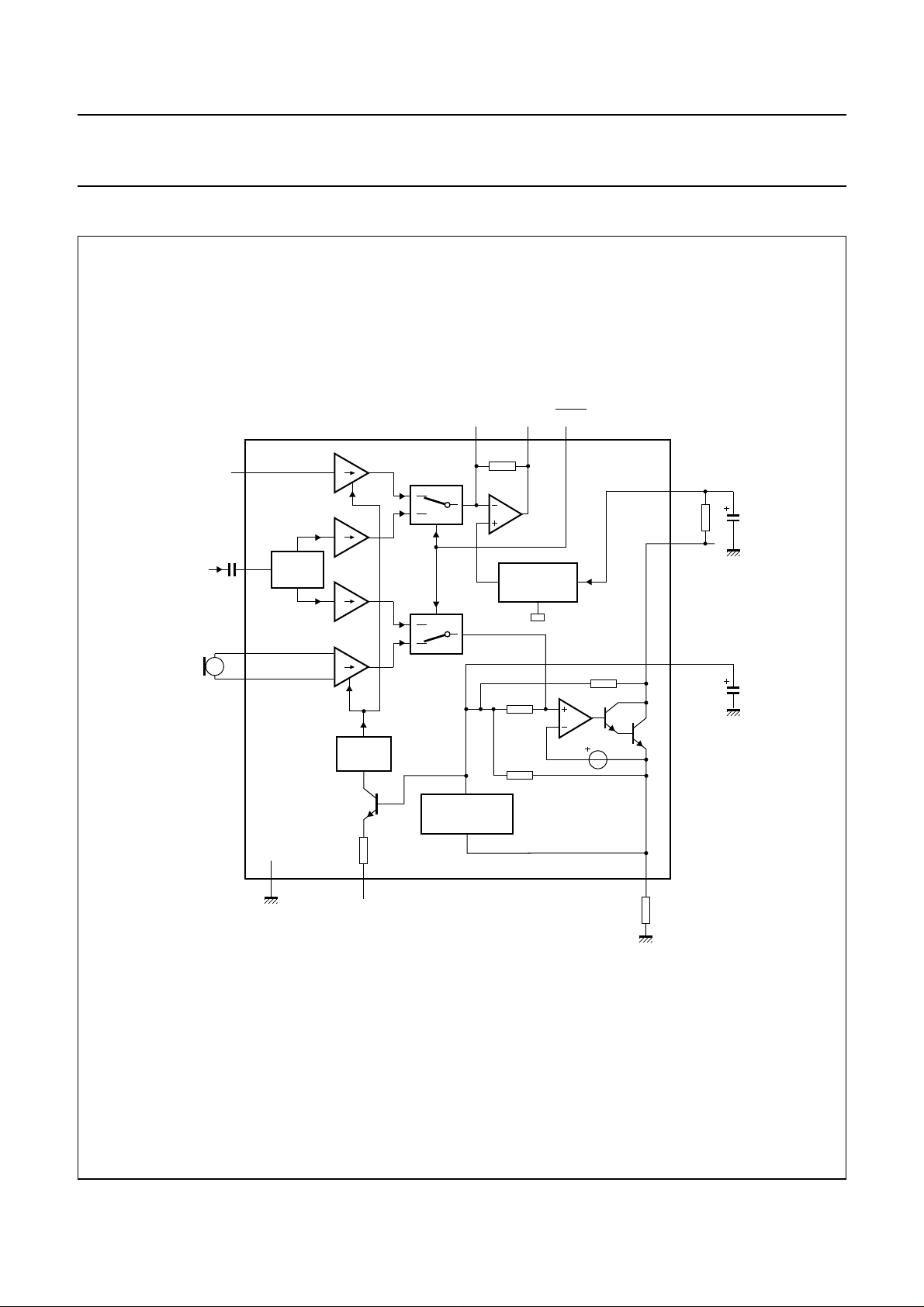
BLOCK DIAGRAM
handbook, full pagewidth
7
DTMF
IR
5
ATT.
V I
V I
V I
GAR
QR MUTE
13 12 6
CURRENT
REFERENCE
TEA1110A
V
14
CC
LN
1
MIC+
MIC−
10
9
V
EE
V I
AGC
CIRCUIT
AGC
LOW VOLTAGE
CIRCUIT
TEA1110A(T)
3
2811
SLPE
REG
MGG736
Fig.1 Block diagram.
2000 Feb 15 3
Philips Semiconductors Product specification
Low voltage versatile telephone
TEA1110A
transmission circuit with dialler interface
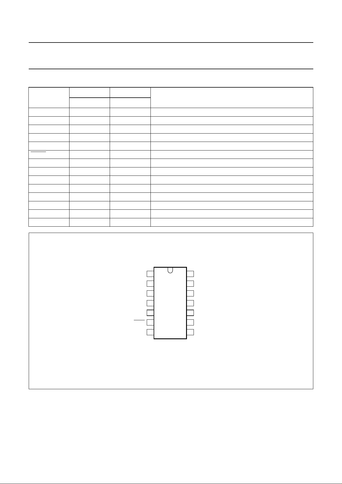
PINNING
SYMBOL
LN 1 1 positive line terminal
SLPE 2 2 slope (DC resistance) adjustment
REG 3 3 line voltage regulator decoupling
n.c. 4 4 not connected
DTMF 5 5 dual-tone multi-frequency input
MUTE 6 6 mute input to select speech or dialling mode (active LOW)
IR 7 7 receiving amplifier input
AGC 8 8 automatic gain control/ line loss compensation
MIC− 9 9 inverting microphone amplifier input
MIC+ 10 10 non-inverting microphone amplifier input
V
EE
QR 12 12 earpiece amplifier output
GAR 13 13 earpiece amplifier gain adjustment
V
CC
PIN PAD
DESCRIPTION
TEA1110A(T) TEA1110AUH
11 11 negative line terminal
14 14 supply voltage for internal circuit
handbook, halfpage
LN
1
SLPE
2
3
REG
4
n.c.
TEA1110A(T)
5
DTMF
6
MUTE
7
IR
MGG735
Fig.2 Pin configuration.
14
V
CC
13
GAR
12
QR
11
V
EE
10
MIC+
9
MIC−
8
AGC
2000 Feb 15 4
Philips Semiconductors Product specification
Low voltage versatile telephone
transmission circuit with dialler interface
FUNCTIONAL DESCRIPTION
All data given in this chapter are typical values, except
when otherwise specified.
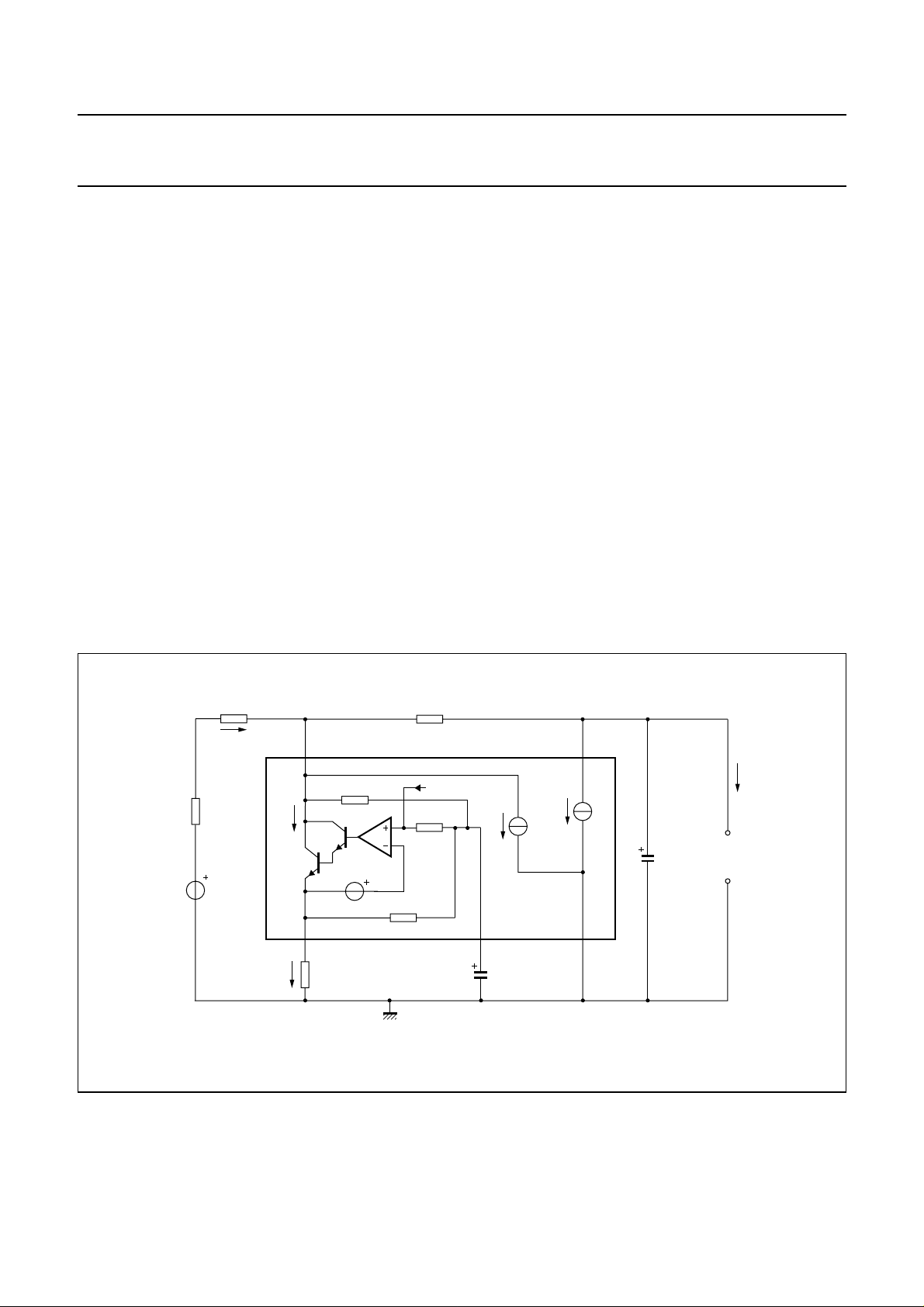
Supply (pins LN, SLPE, VCC and REG)
The supply for the TEA1110A and its peripherals is
obtained from the telephone line; see Fig.3.
The IC generates a stabilized reference voltage (V
between pins LN and SLPE. V
is temperature
ref
compensated and can be adjusted by means of an
external resistor (RVA). V
equals 3.35 V and can be
ref
increased by connecting RVA between pins REG and
SLPE (see Fig.4), or decreased by connecting R
between pins REG and LN. The voltage at pin REG is
used by the internal regulator to generate V
decoupled by C
, which is connected to VEE. This
REG
ref
capacitor, converted into an equivalent inductance
(see Section “Set impedance”), realizes the set
impedance conversion from its DC value (R
SLPE
value (RCC in the audio-frequency range). The voltage at
pin SLPE is proportional to the line current.
ref
VA
and is
) to its AC
)
TEA1110A
The voltage at pin LN is:
V
I
V
LN
SLPEIlineICC
refRSLPEISLPE
Where:
= line current
I
line
ICC= current consumption of the IC
IP= supply current for peripheral circuits
I* = current consumed between LN and VEE.
ThepreferredvalueforR
affect more than the DC characteristics; it also influences
the microphone and DTMF gains, the gain control
characteristics, the sidetone level and the maximum
output swing on the line.
×+=
– IP– I∗–=
is 20 Ω.ChangingR
SLPE
SLPE
will
handbook, full pagewidth
R
exch
V
exch
R
line
I
line
I
SLPE
LN
114
I
sh
V
d
2
SLPE
R
SLPE
20 Ω
R
CC
619 Ω
from pre amp
V
CC
I
I*
311
REG
C
REG
4.7 µF
CC
TEA1110A
C
VCC
100 µF
V
EE
peripheral
circuits
MGG737
I
P
Fig.3 Supply configuration.
2000 Feb 15 5
Philips Semiconductors Product specification
Low voltage versatile telephone
transmission circuit with dialler interface
The internal circuitry of the TEA1110A is supplied from
pin VCC. This voltage supply is derived from the line
voltage by means of a resistor (R
decoupled by a capacitor C
VCC
supply peripheral circuits such as dialling or control
circuits. The V
voltage depends on the current
CC
consumed by the IC and the peripheral circuits as shown
by the formula:
V
CC0
is the internal equivalent resistance of the voltage
R
CCint
supply, and I
V
VLNR
is the current consumed by the output
rec
CC
×–=
CCICC
V
CC0RCCintIPIrec
(see also Figs 5 and 6).
stage of the earpiece amplifier.
The DC line current flowing into the set is determined by
the exchange supply voltage (V
resistance (R
(R
) and the reference voltage (V
line
), the DC resistance of the telephone line
exch
below 7.5 mA, the internal reference voltage (generating
V
)isautomaticallyadjustedtoalowervalue.Thismeans
ref
thatmoresetscanoperateinparallelwithDClinevoltages
(excluding the polarity guard) down to an absolute
minimum voltage of 1.6 V. At currents below 7.5 mA, the
circuit has limited sending and receiving levels. This is
called the low voltage area.
6.0
handbook, halfpage
V
ref
(V)
5.0
) and must be
CC
. It may also be used to
–()×–=
), the feeding bridge
exch
). With line currents
ref
MGD176
TEA1110A
Set impedance
In the audio frequency range, the dynamic impedance is
mainly determined by the R
impedance of the circuit is illustrated in Fig.7.
Microphone amplifier (pins MIC+ and MIC−)
The TEA1110A has symmetrical microphone inputs. The
input impedance between pins MIC+ and MIC− is 64 kΩ
(2 × 32 kΩ). The voltage gain from pins MIC+/MIC− to pin
LN is set at 43.7 dB (typ).
Automatic gain control is provided on this amplifier for line
loss compensation.
Receiving amplifier (pins IR, GAR and QR)
The receiving amplifier has one input (IR) and one output
(QR). The input impedance between pin IR and pin VEEis
20 kΩ. The voltage gain from pin IR to pin QR is set at
33 dB (typ). The gain can be decreased by connecting an
external resistor R
between pins GAR and QR; the
GAR
adjustment range is 14 dB. Two external capacitors C
(connectedbetweenGAR and QR) and C
between GAR and VEE) ensure stability. The C
capacitor provides a first-order low-pass filter. The cut-off
frequency corresponds to the time constant
C
GAR
× (R
GARint
// R
GAR
which sets the gain with a typical value of 125 kΩ. The
condition C
GARS
=10×C
stability.
Theoutputvoltageofthereceivingamplifierisspecifiedfor
continuous wave drive. The maximum output swing
depends on the DC line voltage, the RCC resistor, the I
current consumption of the circuit, the IP current
consumption of the peripheral circuits and the load
impedance.
resistor. The equivalent
CC
GARS
). R
GAR
is the internal resistor
GARint
must be fulfilled to ensure
GAR
(connected
GAR
CC
4.0
(1)
(2)
3.0
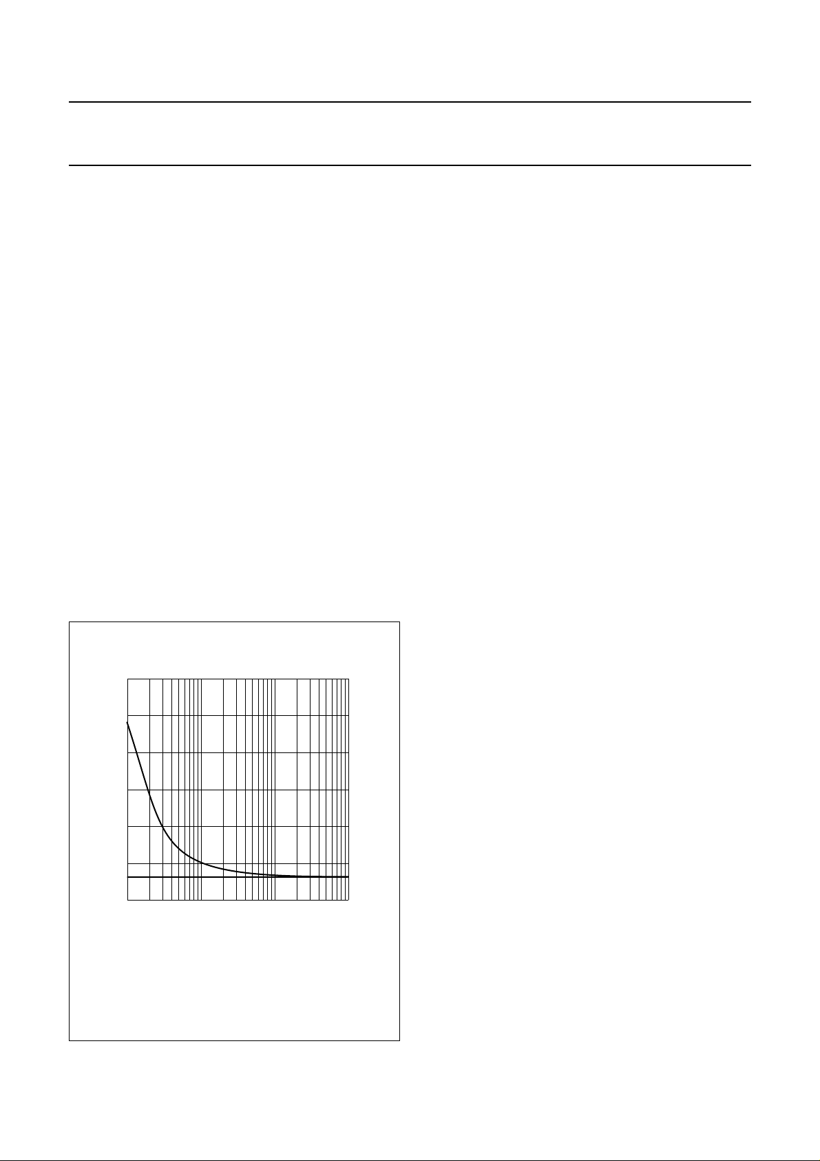
4
10
(1) Influence of RVA on V
(2) V
without influence of RVA.
ref
5
10
.
ref
6
10
RVA (Ω)
7
10
Fig.4 Reference voltage adjustment by RVA.
2000 Feb 15 6
Automatic gain control is provided on this amplifier for line
loss compensation.
Automatic gain control (pin AGC)
The TEA1110A performs automatic line loss
compensation. The automatic gain control varies the gain
of the microphone amplifier and the gain of the receiving
amplifier in accordance with the DC line current. The
control range is 5.9 dB (which corresponds approximately
to a line length of 5 km for a 0.5 mm diameter twisted-pair
copper cable with a DC resistance of 176 Ω/km and an
average attenuation of 1.2 dB/km). The IC can be used
with different configurations of feeding bridge (supply
voltage and bridge resistance) by connecting an external
resistor R
between pins AGC and VEE.
AGC
Philips Semiconductors Product specification
Low voltage versatile telephone
transmission circuit with dialler interface
This resistor enables the I
increased (the ratio between I
by the resistor). The AGC function is disabled when
pin AGC is left open-circuit.
Mute function (pin MUTE)
The mute function performs the switching between the
speechmode and the dialling mode. When MUTE is LOW,
the DTMF input is enabled and the microphone and
receiving amplifiers inputs are disabled. When MUTE is
HIGH, the microphone and receiving amplifiers inputs are
enabled while the DTMF input is disabled. A pull-up
resistor is included at the input.
DTMF amplifier (pin DTMF)
When the DTMF amplifier is enabled, dialling tones may
be sent on line. These tones can be heard in the earpiece
at a low level (confidence tone).
The TEA1110A has an asymmetrical DTMF input. The
input impedance between DTMF and VEE is 20 kΩ. The
voltage gain from pin DTMF to pin LN is 25.3 dB.
start
and I
start
line currents to be
stop
and I
is not affected
stop
2.5
andbook, halfpage
I
P
(mA)
2
1.5
1
0.5
0
01234
(1) With RVA resistor.
(2) Without RVA resistor.
TEA1110A
MBE783
(1)(2)
VCC (V)
The automatic gain control has no effect on the DTMF
amplifier.
handbook, halfpage
R
CCintVCC
V
CCO
I
rec
V
EE
PERIPHERAL
CIRCUIT
I
P
MBE792
Fig.5 Typical current IP available from VCC for
peripheral circuits at I
andbook, halfpage
V
Leq=C
RP= internal resistance.
RP= 15.5 kΩ.
REG
× R
LN
SLPE
EE
SLPE
× RP.
L
EQ
V
R
SLPE
20 Ω
ref
= 15 mA.
line
R
P
REG V
C
REG
4.7 µF
R
619 Ω
CC
C
100 µF
MBE788
CC
VCC
Fig.6 VCC supply voltage for peripherals.
2000 Feb 15 7
Fig.7 Equivalent impedance between LN and
VEE.
Philips Semiconductors Product specification
Low voltage versatile telephone
transmission circuit with dialler interface
SIDETONE SUPPRESSION
The TEA1110A anti-sidetone network comprising
RCC//Z
suppresses the transmitted signal in the earpiece.
Maximum compensation is obtained when the following
conditions are fulfilled:
R
k
Z
bal
The scale factor k is chosen to meet the compatibility with
a standard capacitor from the E6 or E12 range for Z
In practice, Z
thelinelength. Therefore, the value of Z
average line length which gives satisfactory sidetone
suppression with short and long lines. The suppression
also depends on the accuracy of the match between Z
and the impedance of the average line.
, R
, R
line
ast1
× R
SLPERast1
R
ast2Rast3RSLPE
=
------------------------------------------------------------------R
ast1RSLPE
kZ
×=
line
line
, R
ast2
CC
+()×()
×()
varies considerably with the line type and
, R
ast3
R
ast2Rast3
SLPE
+()×=
and Z
bal
shouldbefor an
bal
(see Fig.8 )
bal
.
bal
TEA1110A
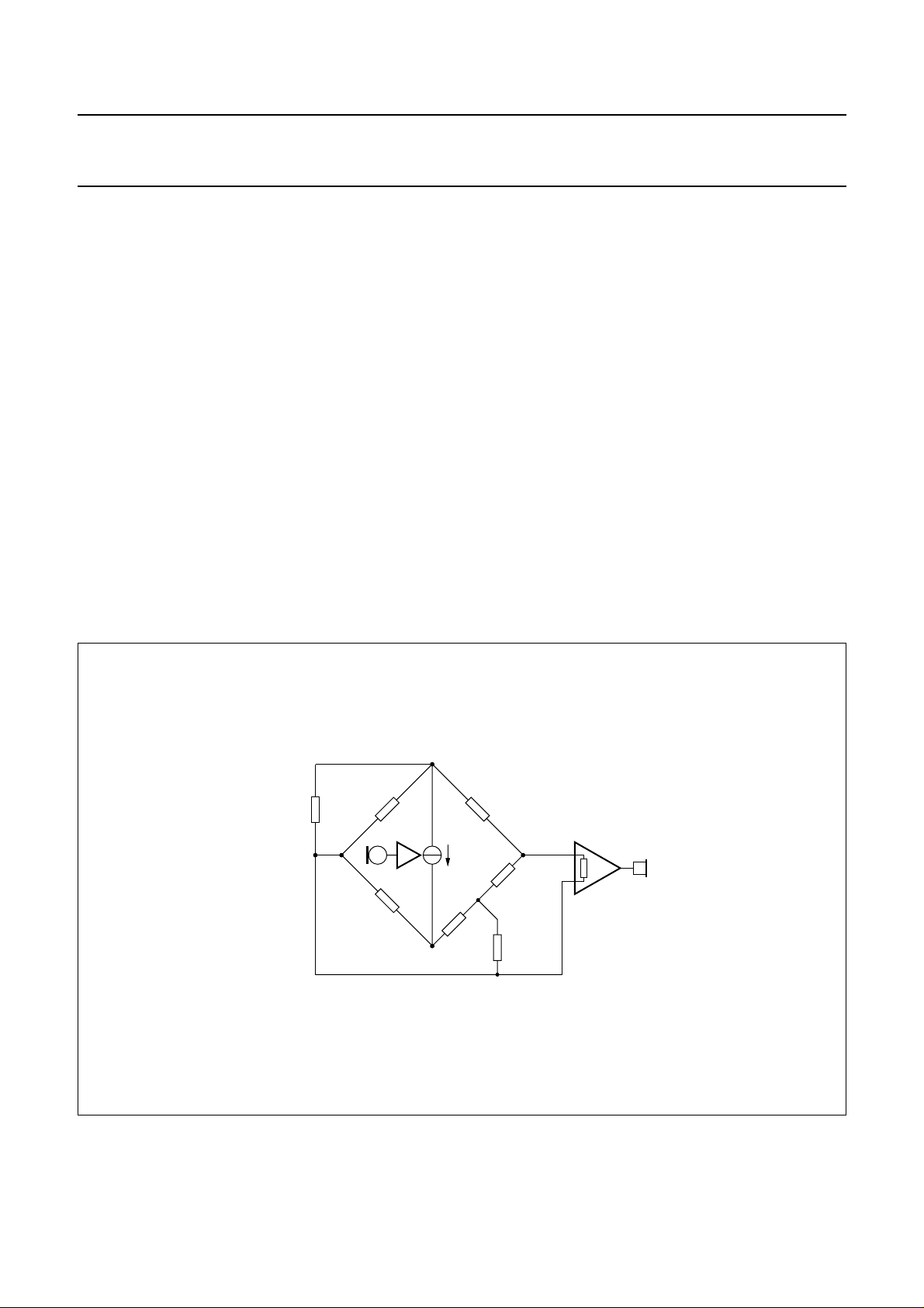
The anti-sidetone network for the TEA1110A (as shown in
Fig.13) attenuates the receiving signal from the line by
32 dB before it enters the receiving amplifier. The
attenuation is almost constant over the whole audio
frequency range.
A Wheatstone bridge configuration (see Fig.9) may also
be used.
More information on the balancing of an anti-sidetone
bridge can be obtained in our publication
Handbook for Wired Telecom Systems, IC03b”
number 9397 750 00811.
“Applications
, order
handbook, full pagewidth
LN
R
R
SLPE
CC
SLPE
Z
line
V
EE
R
ast1
I
m
R
ast3
IR
Z
R
ast2
Z
bal
ir
MBE787
Fig.8 Equivalent circuit of TEA1110A family anti-sidetone bridge.
2000 Feb 15 8
 Loading...