

Philips TEA1098TV-C2, TEA1098TV-C1, TEA1098H-C2, TEA1098H-C1 Datasheet

DATA SH EET
Product specification
Supersedes data of 1999 May 20
File under Integrated Circuits, IC03
1999 Oct 14
INTEGRATED CIRCUITS
TEA1098
Speech and handsfree IC
1999 Oct 14 2
Philips Semiconductors Product specification
Speech and handsfree IC TEA1098
FEATURES
Line interface
• Low DC line voltage
• Voltage regulator with adjustable DC voltage
• Symmetrical high impedance inputs (70 kΩ) for
dynamic, magnetic or electret microphones
• DTMF input with confidence tone on earphone and/or
loudspeaker
• Receive amplifier for dynamic, magnetic or
piezo-electric earpieces(with externally adjustable gain)
• Automatic Gain Control (AGC) for true line loss
compensation.
Supplies
• Provides a strong 3.35 V regulated supply for
microcontrollers or diallers
• Provides filtered power supply, optimized according to
line current
• Filtered 2.0 V power supply output for electret
microphone
• PD logic input for power-down.
Handsfree
• Asymmetrical high input impedance for electret
microphone
• Loudspeaker amplifier with single-ended rail-to-rail
output and externally adjustable gain
• Dynamic limiter on loudspeaker amplifier to prevent
distortion
• Logarithmic volume controlon loudspeakeramplifier via
linear potentiometer
• Duplex controller consisting of:
– Signal and noise envelope monitors for both
channels (with adjustable sensitivities and timing)
– Decision logic (with adjustable switch-over and Idle
mode timing)
– Voice switch control (with adjustable switching range
and constant sum of gain during switching).
APPLICATIONS
• Line powered telephone sets.
GENERAL DESCRIPTION
The TEA1098 is an analog bipolar circuit dedicated to
telephonyapplications. It includesa line interface,handset
(HS) microphone and earpiece amplifiers, handsfree (HF)
microphone and loudspeaker amplifiers and a duplex
controller with signal and noise monitors on both channels.
This IC provides a 3.35 V supply for a microcontroller or
dialler and a 2.0 V filtered voltage supply for an electret
microphone.
ORDERING INFORMATION
TYPE
NUMBER
PACKAGE
NAME DESCRIPTION VERSION
TEA1098TV VSO40 plastic very small outline package; 40 leads SOT158-1
TEA1098H QFP44 plastic quad flat package; 44 leads (lead length 1.3 mm);
body 10 × 10 × 1.75 mm
SOT307-2
TEA1098UH − bare die; on foil −
1999 Oct 14 3
Philips Semiconductors Product specification
Speech and handsfree IC TEA1098
QUICK REFERENCE DATA
I
line
= 15 mA; R
SLPE
=20Ω; Z
line
= 600 Ω; f = 1 kHz; T
amb
=25°C for TEA1098H and TEA1098TV; Tj=25°C for
TEA1098UH; AGC pin connected to LN;
PD = HIGH; HFC = LOW; MUTE = HIGH; measured according to test circuits;
unless otherwise specified.
SYMBOL PARAMETER CONDITIONS MIN. TYP. MAX. UNIT
I
line
line current operating range normal operation 11 − 130 mA
with reduced performance 1 − 11 mA
V
SLPE
stabilized voltage between SLPE
and GND
I
line
= 15 mA 3.4 3.7 4.0 V
I
line
= 70 mA 5.7 6.1 6.5 V
V
BB
regulated supply voltage for
internal circuitry
I
line
= 15 mA 2.75 3.0 3.25 V
I
line
= 70 mA 4.9 5.3 5.7 V
V
DD
regulated supply voltage on pin
V
DD
VBB> 3.35 V + 0.25 V (typ.) 3.1 3.35 3.6 V
otherwise − V
BB
− 0.25 − V
I
BB
current available on pin V
BB
in speech mode − 11 − mA
in handsfree mode − 9 − mA
I
BB(pd)
current consumption on V
BB
during power-down phase
PD = LOW − 460 −µA
G
v(MIC-LN)
voltage gain from pin MIC+/MIC−
to LN
V
MIC
= 5 mV (RMS) 43.3 44.3 45.3 dB
G
v(IR-RECO)
voltage gain from pin IR
(referenced to LN) to RECO
VIR= 8 mV (RMS) 28.7 29.7 30.7 dB
∆G
v(QR)
gain voltage range between pins
RECO and QR
−3 − +15 dB
G
v(TXIN-TXOUT)
voltage gain from pin TXIN to
TXOUT
V
TXIN
= 3 mV (RMS);
R
GATX
= 30.1 kΩ
12.7 15.2 17.7 dB
G
v(HFTX-LN)
voltage gain from pin HFTX to LN V
HFTX
= 15 mV (RMS) 33.5 34.7 35.9 dB
G
v(HFRX-LSAO
) voltage gain from pin HFRX
to LSAO
V
HFRX
= 30 mV (RMS);
R
GALS
= 255 kΩ; I
line
=70mA
25.5 28 30.5 dB
SWRA switching range − 40 − dB
∆SWRA switching range adjustment with R
SWR
referenced to
365 kΩ
−40 − +12 dB
∆G
v(trx)
gain control range for transmitand
receive amplifiers affected by the
AGC; with respect to I
line
=15mA
I
line
= 70 mA 5.45 6.45 7.45 dB
1999 Oct 14 4
Philips Semiconductors Product specification
Speech and handsfree IC TEA1098
BLOCK DIAGRAM
MGL317
LINE CURRENT DETECTION
LOW VOLTAGE BEHAVIOUR
SUPPLY
MANAGEMENT
SWITCH
STARTER
AGC
GND
V
BB
V
DD
MICS
PD
AGC
LN 18 (15)
21 (18)
16 (13)
39 (36)
35 (32)
34 (31)
33 (30)
31 (28)
8 (4)
7 (3)
6 (2)
9 (5)
11 (7)
10 (6)
14 (11)
15 (12)
12 (8)
38 (35)
(17) 20
(1) 5
(23) 26
(22) 25
(21) 24
(25) 28
(24) 27
(29) 32
(26) 29
(27) 30
(39) 2
(37) 40
(38) 1
(20) 23
(19) 22
(10) 13
37 (34)
36 (33)
REG
19
(16)17(14)
SLPE
Tail currents for preamps
POWER-DOWN
CURRENT SOURCES
ATTENUATOR
HFTX
MIC+
MIC−
DTMF
LOGIC
INPUTS
DECODING
HFC
MUTE
GATX
TXOUT
SWT
GNDTX
TXIN
TEA1098
TX AND RX
ENVELOPE AND NOISE
DETECTORS
TSEN
TENV
TNOI
RNOI
RENV
RSEN
LSAO
GALS
BUFFERS
AND
COMPARATORS
DUCO LOGIC
SWT STATUS
VOICE
SWITCH
VOLUME
CONTROL
IDT
STAB
SWR
VOL
HFRX
ATTENUATOR
DLC
DYNAMIC
LIMITER
IR
RECO
QR
GARX
R1
Fig.1 Block diagram.
Pin numbers in parenthesis apply to the TEA1098H. Pin numbers not in parenthesis apply to the TEA1098TV.
1999 Oct 14 5
Philips Semiconductors Product specification
Speech and handsfree IC TEA1098
PINNING
SYMBOL
PIN PAD
DESCRIPTION
TEA1098TV TEA1098H TEA1098UH
PD 1 38 41 power-down input (active LOW)
MUTE 2 39 42 logic input (active LOW)
n.c. 3 40 43 not connected
n.c. 4 41 44 not connected
n.c. − 42 45 not connected
n.c. − 43 46 not connected
n.c. − 44 47 not connected
HFRX 5 1 1 receive input for loudspeaker amplifier
TNOI 6 2 2 transmit noise envelope timing adjustment
TENV 7 3 3 transmit signal envelope timing adjustment
TSEN 8 4 4 transmit signal envelope sensitivity adjustment
RNOI 9 5 5 receive noise envelope timing adjustment
RSEN 10 6 6 receive signal envelope sensitivity adjustment
RENV 11 7 7 receive signal envelope timing adjustment
DLC 12 8 8 dynamic limiter capacitor for the loudspeaker amplifier
n.c. − 9 9 and 13 not connected
V
BB
13 10 10 stabilized supply for internal circuitry
GALS 14 11 11 loudspeaker amplifier gain adjustment
LSAO 15 12 12 loudspeaker amplifier output
GND 16 13 14 and 15 ground reference
SLPE 17 14 16 line current sense
LN 18 15 17 positive line terminal
REG 19 16 18 line voltage regulator decoupling
IR 20 17 19 receive amplifier input
AGC 21 18 20 automatic gain control/line loss compensation
V
DD
22 19 21 3.35 V regulated voltage supply for microcontrollers
MICS 23 20 22 microphone supply
STAB 24 21 23 reference current adjustment
SWR 25 22 24 switching range adjustment
VOL 26 23 25 loudspeaker volume adjustment
SWT 27 24 26 switch-over timing adjustment
IDT 28 25 27 Idle mode timing adjustment
TXOUT 29 26 28 HF microphone amplifier output
GATX 30 27 29 HF microphone amplifier gain adjustment
TXIN 31 28 30 HF microphone amplifier input
GNDTX 32 29 31 to 32 ground reference for microphone amplifiers
MIC− 33 30 33 negative HS microphone amplifier input
MIC+ 34 31 34 positive HS microphone amplifier input
1999 Oct 14 6
Philips Semiconductors Product specification
Speech and handsfree IC TEA1098
DTMF 35 32 35 dual tone multi-frequency input
QR 36 33 36 earpiece amplifier output
GARX 37 34 37 earpiece amplifier gain adjustment
RECO 38 35 38 receive amplifier output
HFTX 39 36 39 transmit input for line amplifier
HFC 40 37 40 logic input
SYMBOL
PIN PAD
DESCRIPTION
TEA1098TV TEA1098H TEA1098UH
handbook, halfpage
TEA1098TV
MGL341
1
2
3
4
5
6
7
8
9
10
11
12
13
14
15
16
17
18
19
20
40
39
38
37
36
35
34
33
32
31
30
29
28
27
26
25
24
23
22
21
HFC
HFTX
RECO
GARX
QR
DTMF
MIC+
MIC−
GNDTX
TXIN
GATX
TXOUT
IDT
SWT
VOL
SWR
STAB
MICS
V
DD
AGC
PD
MUTE
n.c.
n.c.
HFRX
TNOI
TENV
TSEN
RNOI
RSEN
RENV
DLC
V
BB
GALS
LSAO
GND
SLPE
LN
REG
IR
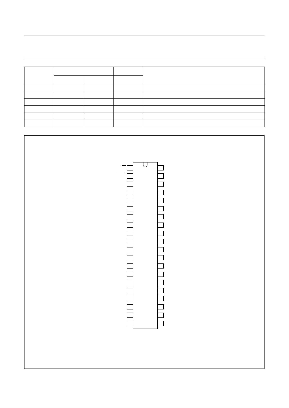
Fig.2 Pin configuration (TEA1098TV).
1999 Oct 14 7
Philips Semiconductors Product specification
Speech and handsfree IC TEA1098
handbook, full pagewidth
1
2
3
4
5
6
7
8
9
10
11
33
32
31
30
29
28
27
26
25
24
23
12
13
14
15
16
17
18
19
20
21
22
44
43
42
41
40
39
38
37
36
35
34
TEA1098H
FCA020
QR
DTMF
MIC+
MIC−
TXIN
GATX
TXOUT
IDT
SWT
VOL
HFRX
TNOI
TENV
TSEN
RNOI
RSEN
DLC
n.c.
GALS
GNDTX
n.c.
n.c.
n.c.
n.c.
MUTE
PD
HFTX
RECO
GARX
n.c.
HFC
GND
SLPE
LN
REG
IR
AGC
MICS
STAB
SWR
LSAO
V
DD
RENV
V
BB
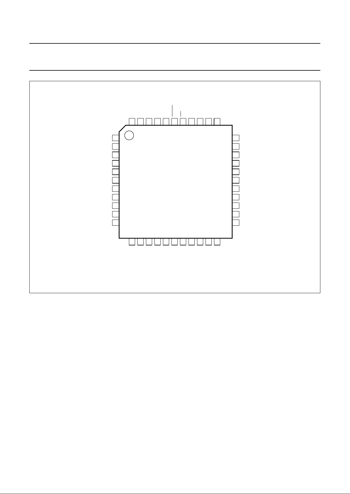
Fig.3 Pin configuration (TEA1098H).
FUNCTIONAL DESCRIPTION
All data values given in this chapter are typical, except
when otherwise specified.
Supplies
LINE INTERFACE AND INTERNAL SUPPLY (PINS LN, SLPE,
REG AND VBB)
Thesupply for theTEA1098 and itsperipheralsis obtained
from the line. The IC generates a stabilized reference
voltage (V
ref
) between pins SLPE and GND.
This reference voltage is equal to 3.7 V for line currents
below 18 mA. When the line current rises above 45 mA,
the reference voltage rises linearly to 6.1 V. For line
currents below 9 mA, V
ref
is automatically adjusted to a
lower value. The performance of the TEA1098 in this
so-called low voltage area is limited (see Section “Low
voltage behaviour”). The reference voltage is temperature
compensated.
The voltage between pins SLPE and REG is used by the
internal regulator to generate the stabilized reference
voltage and is decoupled by a capacitor connected
between pins LN and REG. This capacitor, converted into
an equivalent inductance realizes the set impedance
conversionfrom its DC value(R
SLPE
)to its AC value(done
by an external impedance).
The IC regulates the line voltage at pin LN which can be
calculated as follows:
where:
I
line
= line current.
Ix= current consumed on pin LN (approximately a
few µA).
I
SLPE
= current flowing through the R
SLPE
resistor.
V
LN
V
refRSLPEISLPE
×+=
I
SLPEIline
Ix–=
1999 Oct 14 8
Philips Semiconductors Product specification
Speech and handsfree IC TEA1098
The preferred value for R
SLPE
is 20 Ω. Changing this value
not only affects the DC characteristics, it also influences
the transmit gains to the line, the gain control
characteristic,the sidetonelevel, and themaximum output
swing on the line.
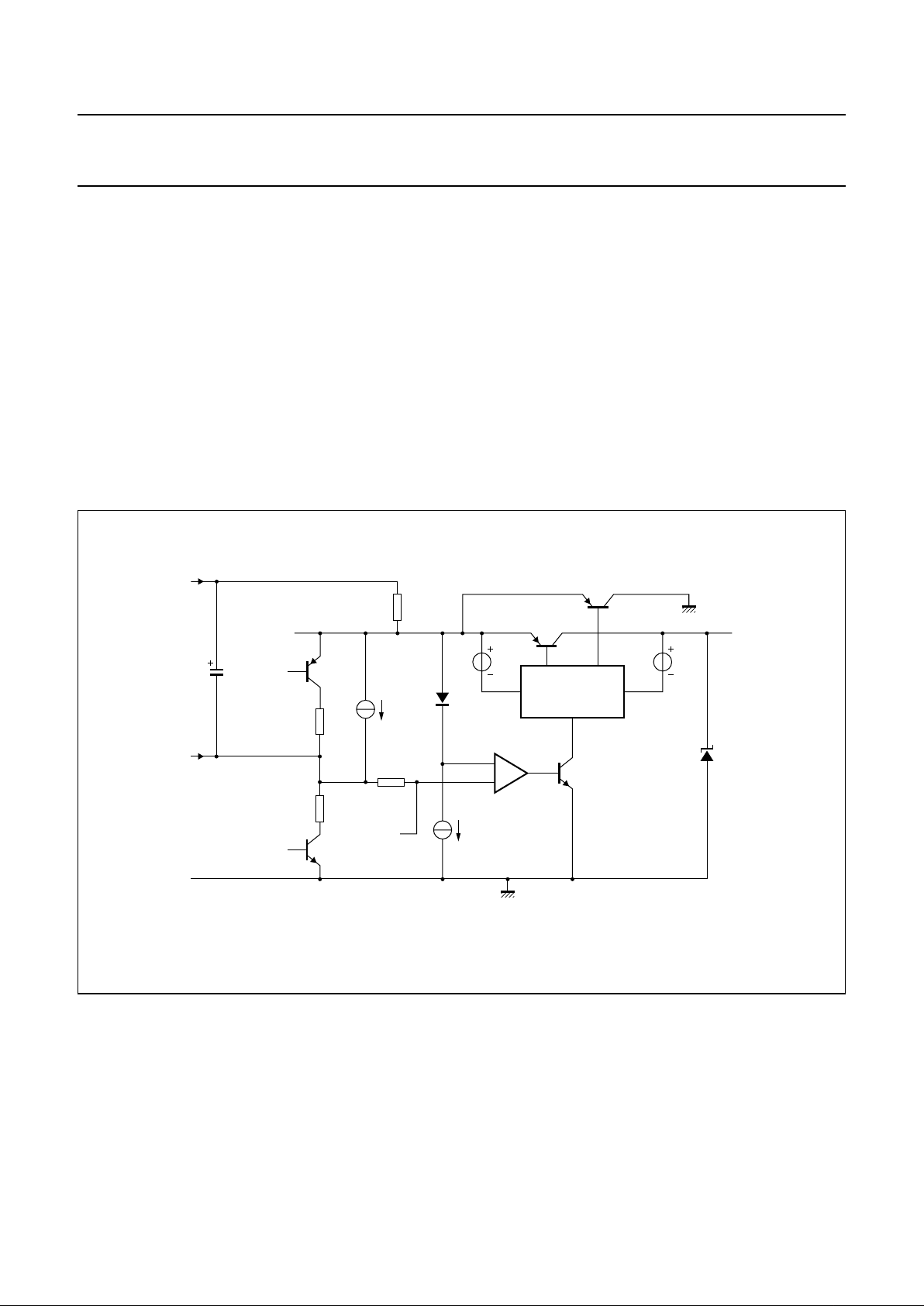
Figure 4 shows that the internal circuit is supplied by pin
VBB, which combined with the line interface is a strong
supply point.
The line current through resistor R
SLPE
is sunk by the V
BB
voltage stabilizer, and is suitable for supplying a
loudspeaker amplifier or any peripheral IC. Voltage VBBis
3.0 V at line currents below 18 mA and rises linearly to
5.3 V when the line current rises above 45 mA. It is
temperature compensated.
The current switch TR1-TR2 is intended to reduce
distortionof large AC linesignals. Current I
SLPE
issupplied
to VBB via TR1 when the voltage on pin SLPE is above
VBB+ 0.25 V. Whenthe voltage on pin SLPE is below this
value, I
SLPE
is shunted to GND via TR2.
Voltage V
ref
can be increased by connecting an external
resistor between pins REG and SLPE. For large line
currents, this increase can slightly affect some dynamic
performances such as maximumsignal level on the line at
2% Total Harmonic Distortion(THD). Theexternal resistor
does not affect the voltage on pin VBB; see Fig.5 for the
main DC voltages.
handbook, full pagewidth
MGM298
TN2
TR2
TR1
E2
D1
D1
R3
R2
R1
TN1
TP1
J2
J1
E1
GND
GND
V
BB
from
preamp
GND
REG
LN
SLPE
C
REG
4.7 µF
R
SLPE
20 Ω
Fig.4 Line interface principle.
1999 Oct 14 9
Philips Semiconductors Product specification
Speech and handsfree IC TEA1098
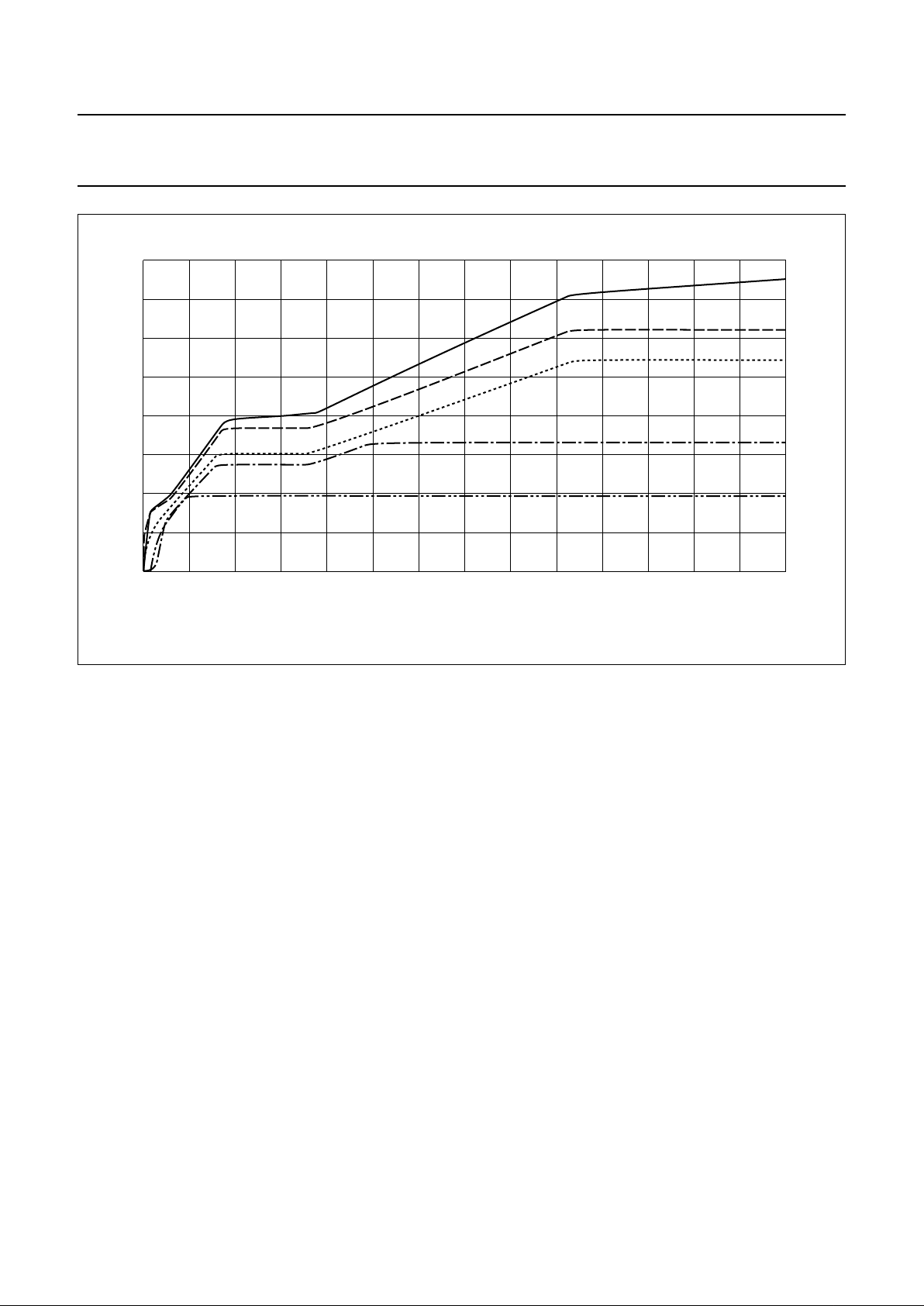
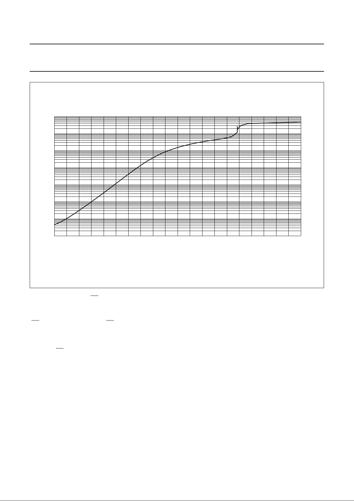
handbook, full pagewidth
0.070.06
8
6
2
0
0 0.01
voltages
(V)
0.02 0.05
MICS
V
DD
V
BB
SLPE
LN
I
line
(A)
0.040.03
4
FCA049
Fig.5 Main DC voltages.
V
DD
SUPPLY FOR MICROCONTROLLERS (PIN V
DD
)
The voltage on the V
DD
supply point follows the voltage on
VBBwith a difference typically of 250 mV, internallylimited
to 3.35 V. This voltage is temperature compensated.
This supply point can provide a current of up to typically
3 mA. Its internal consumption stays low (a few 10 nA) as
long as VDD does not exceed 1.5 V (see Fig.6).
An external voltage can be connected to VDD with limited
extra consumptionon VDD(typically 100 µA).This voltage
source should not be below 3.5 V or above 6 V.
VBBand VDDcan supply current to external circuits within
the line limits, taking into account the internal current
consumption.
S
UPPLY FOR MICROPHONE (PINS MICS AND GNDTX)
The MICS output can be used as a supply for an electret
microphone. Its voltage is equal to 2.0 V; it can source a
current of up to 1 mA and has an output impedance equal
to 200 Ω.
L
OW VOLTAGE BEHAVIOUR
For line currents below 9 mA, the reference voltage is
automatically adjusted to a lower value; the VBB voltage
follows the SLPE voltage with a difference of 250 mV.
Any excess current available, other than for the purposes
of DC biasing the IC, will be small. At low reference
voltage, the IC has limited performance.
When voltage VBB falls below 2.7 V, it is detected by the
receive dynamic limiter circuit connected to pin LSAOand
is continuously activated, discharging the capacitor
connected to pin DLC. In the DC condition, the
loudspeaker is then automatically disabled below this
voltage.
When VBBfalls below 2.5 V, the TEA1098 is forced into a
lowvoltage mode irrespectiveof the logicinput levels. This
is a speech mode with reduced performance which only
enables the microphone channel (between the MICinputs
and pin LN) and the earpiece amplifier. These two
channels are able to deliver signals for line currents as
small as 3 mA. The HFC input is tied to GND sinking a
current of typically 300 µA.
1999 Oct 14 10
Philips Semiconductors Product specification
Speech and handsfree IC TEA1098
handbook, full pagewidth
1.0
I
DD
(pA)
1.5 2.5 3.0
VDD (V)
2.0
10
8
10
7
10
6
10
5
10
4
10
3
10
2
10
FCA050
Fig.6 Current consumption on VDD.
POWER-DOWN MODE (PIN PD)
To reduce consumption during dialling or register recall
(flash), the TEA1098 is provided with a power-down input
(PD). When the voltage on pin PD is LOW, the current
consumption from VBB and VDD is reduced to typically
460 µA. Therefore a capacitor of 470 µF on VBB is
sufficient to power the TEA1098 during pulse dialling or
flash. The PD input has a pull-up structure. In this mode,
the capacitor C
REG
is internally disconnected.
Transmit channels (pins MIC+, MIC−, DTMF,
HFTX and LN)
HANDSET MICROPHONE AMPLIFIER (PINS MIC+, MIC−
AND LN)
The TEA1098 has symmetrical microphone inputs.
The input impedance between pins MIC+ and MIC− is
typically70 kΩ.The voltage gainbetweenpinsMIC+/MIC−
and LN is set to 44.3 dB. Without output limitation, the
microphone input stage can accept signals of up to
18 mV (RMS) at 2% THD (room temperature).
The microphone inputs are biased at a voltage of one
diode.
Automatic gain control is provided for line loss
compensation.
DTMF AMPLIFIER (PINS DTMF, LN AND RECO)
TheTEA1098 has anasymmetrical DTMF input.The input
impedance between DTMF and GND is typically 20 kΩ.
The voltage gain between pins DTMF and LN is set to
25.35 dB. Without output limitation, the input stage can
accept signals of up to 180 mV (RMS) at 2% THD (room
temperature).
When the DTMF amplifier is enabled, dialling tones may
be sent on the line. These tones can be heard in the
earpiece or in the loudspeaker ata lowlevel. This is called
theconfidence tone. Thevoltageattenuation between pins
DTMF and RECO is typically −16.5 dB. This input is
DC biased at 0 V.
The automatic gain control has no effect on these
channels.

1999 Oct 14 11
Philips Semiconductors Product specification
Speech and handsfree IC TEA1098
HANDSFREE TRANSMIT AMPLIFIER (PINS HFTX AND LN)
The TEA1098 has an asymmetrical HFTX input, which is
mainly intended for use in combination with the TXOUT
output. The input impedance between HFTX and GND is
typically 20 kΩ. The voltage gain between
pins HFTX and LN is set to 34.7 dB. Without output
limitation, the input stage can accept signals of up to
95 mV (RMS) at 2% THD (room temperature). The HFTX
input is biased at a voltage of two diodes.
Automatic gain control is provided for line loss
compensation.
Receive channels (pins IR, RECO, GARX and QR)
RX AMPLIFIER (PINS IR AND RECO)
The receive amplifier has one input (IR) which is
referenced to the line. The input impedance between pins
IR and LN is typically 20 kΩ and the DC bias between
these pins is equal to the voltage of one diode. The gain
between pins IR(referenced to LN) and RECO is typically
29.7 dB. Without output limitation, the input stage can
accept signals of up to 50 mV (RMS) at 2% THD (room
temperature).
The receive amplifier has a rail-to-rail output (RECO),
which is designed for use with high ohmic (real) loads of
more than 5 kΩ. This output is biased at a voltage of two
diodes.
Automatic gain control is provided for line loss
compensation.
EARPIECE AMPLIFIER (PINS GARX AND QR)
The earpiece amplifier is an operational amplifier which
has an output (QR) and an inverting input (GARX).
Its input signal is fed by a decoupling capacitor from the
receive amplifier output (RECO) to two resistorswhich set
the required gain or attenuation from −3 to +15 dB
compared to the receive gain.
Two external capacitors C
GAR
(connected between GAR
and QR) and C
GARS
(connected between GAR and GND)
ensure stability. The C
GAR
capacitor provides a first-order
low-pass filter. The cut-off frequency corresponds to the
time constant C
GAR
× Re2. The relationship
C
GARS
≥ 10 × C
GAR
must be satisfied.
The earpiece amplifierhas arail-to-rail output(QR) biased
at a voltage of two diodes. It is designed for use with low
ohmic (real) loads of 150 Ω, or capacitive loads of 100 nF
in series with 100 Ω.
AGC (pin AGC)
The TEA1098 performsautomatic lineloss compensation,
which fits well with the true line attenuation. The automatic
gain control varies the gain of some transmit and receive
amplifiers in accordance with the DC line current.
The controlrange is6.45 dB for G
v(MIC-LN)
andG
v(IR-RECO),
and 6.8 dB for G
v(HFTX-LN)
, which corresponds
approximately to a line length of 5.5 km for a 0.5 mm
twisted-pair copper cable.
To enable this gain control, the pin AGC must be shorted
to pin LN. The start current forcompensation corresponds
to a line current of typically 23 mA and a stop current of
57 mA. The start current can be increased by connecting
an external resistor between pins AGC and LN. It can be
increased by up to 40 mA (using a resistor of typically
80 kΩ). The start and stop current will be maintained at a
ratio of 2.5. By leaving the AGC pin open, the gain control
is disabled and no line loss compensation occurs.
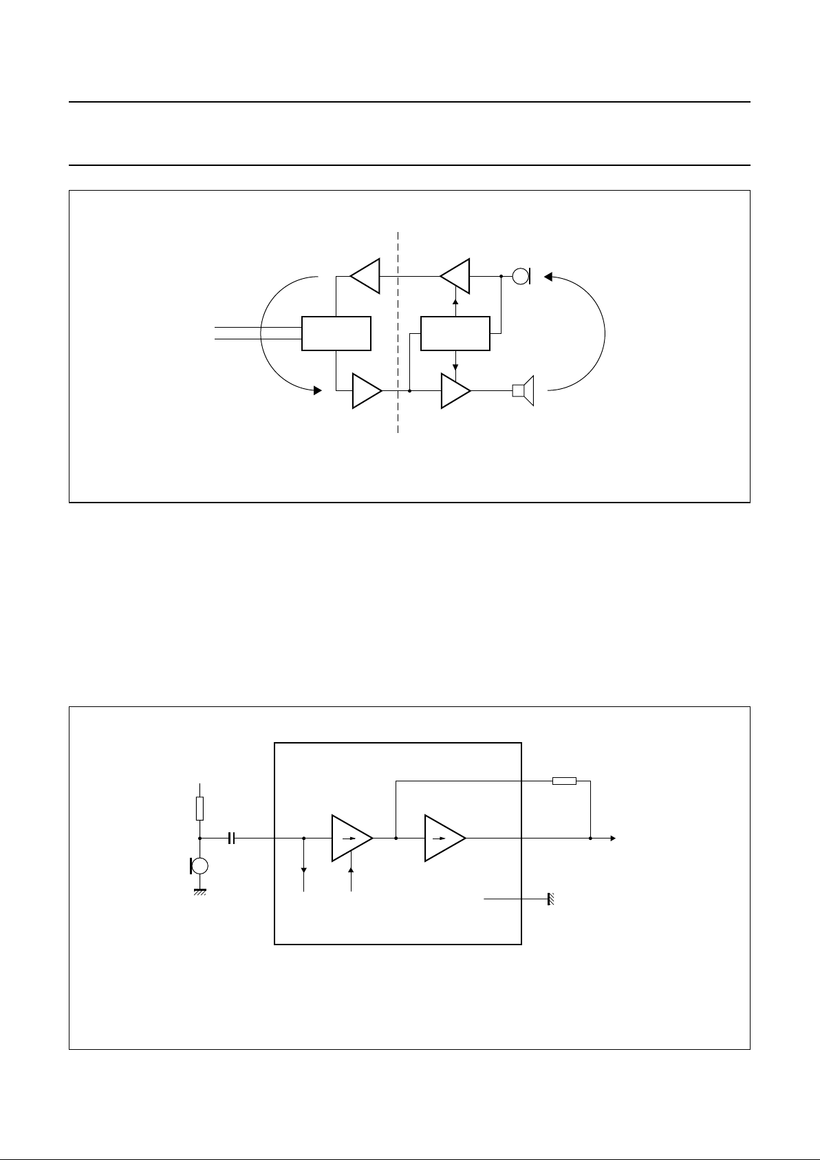
Handsfree application
Figure 7 shows a loop is formed by the sidetone network
in the line interface section, and by the acoustic coupling
between loudspeaker and microphone in the handsfree
section. A loop-gain of greater than 1 causes howl.
To prevent howl in full duplex applications, the loop-gain
must be set much lower than 1. This is achieved by the
duplex controller which detects the channel with the
‘largest’ signal and controls the gains of the microphone
and the loudspeaker amplifiers so that the sum of their
gains remains constant.
Thereforein the handsfreeapplication,thecircuit can have
three stable modes:
1. Transmit mode (Tx mode).
The microphone amplifieris atmaximum gain, andthe
loudspeaker amplifier is at minimum gain.
2. Receive mode (Rx mode).
The microphoneamplifier is at minimum gain, and the
loudspeaker amplifier is at maximum gain.
3. Idle mode.
The microphone amplifier and the loudspeaker
amplifier are both midway between maximum and
minimum gain.
The difference between the maximum and minimum gain
is called the switching range.
1999 Oct 14 12
Philips Semiconductors Product specification
Speech and handsfree IC TEA1098
handbook, full pagewidth
MGM299
DUPLEX
CONTROL
HYBRID
telephone
line
sidetone
acoustic
coupling
Fig.7 Handsfree telephone set principles.
HANDSFREE MICROPHONE CHANNEL: PINS TXIN, GATX,
TXOUT AND GNDTX (see Fig.8)
TheTEA1098 has an asymmetricalhandsfreemicrophone
input (TXIN) with an input resistance of 20 kΩ.
The input DCbias is 0 V.Thegain oftheinput stage varies
according to the TEA1098 mode. In Tx mode, it has
maximum gain; in Rx mode, it has minimum gain, and in
Idle mode, it is midway between maximum and minimum
gain.
Switch-over from one mode to the other is smooth and
click-free. The output (TXOUT) is biased at a voltage of
two diodes and has a current capability of 20 µA (RMS).
In Tx mode, the overall gain of the microphone amplifier
(from pins TXIN to TXOUT) can be adjusted from
0 up to 31 dB to suit specific application requirements.
The gain is proportional to the value of R
GATX
and equals
15.2 dB whenR
GATX
is 30.1 kΩ. Withoutoutput limitation,
the microphone input stage can accept signals of up to
18 mV (RMS) at 2% THD (room temperature).
handbook, full pagewidth
MGL342
V I I V
C
MIC
V
BB
R
MIC
TXIN
from
voice
switch
to
envelope
detector
GNDTX
TXOUT
GATX
31
(28)
30
(27)
29
(26)
32
(29)
R
GATX
Fig.8 Handsfree microphone channel.
Pin numbers in parenthesis apply to the TEA1098H. Pin numbers not in parenthesis apply to the TEA1098TV.
 Loading...