

Philips TEA1098A Datasheet

INTEGRATED CIRCUITS
DATA SH EET
TEA1098A
Speech and handsfree IC
Preliminary specification
File under Integrated Circuits, IC03
2000 Mar 21

Philips Semiconductors Preliminary specification
Speech and handsfree IC TEA1098A
FEATURES
Line interface
• Low DC line voltage
• Voltage regulator with adjustable DC voltage
• Symmetrical high impedance inputs (70 kΩ) for
dynamic, magnetic or electret microphones
• DTMF input with confidence tone on earphone and/or
loudspeaker
• Earphone amplifier for dynamic, magnetic or
piezo-electric earpieces(with externally adjustable gain)
• Digital volume control on earphone amplifier (4 steps)
• Automatic Gain Control (AGC) for true line loss
compensation
• Microphone mute
• Key tone mode.
Supplies
• Provides a strong 3.35 V regulated supply for
microcontroller or dialler
• Provides filtered power supply, optimized according to
line current
• Filtered 2.0 V power supply output for electret
microphone
• PD logic input for power-down.
• Duplex controller consisting of:
– signaland noise envelopemonitorsfor bothchannels
(with adjustable sensitivities and timing)
– decision logic (with adjustable switch-over and Idle
mode timing)
– voice switch control (with adjustable switching range
and constant sum of gain during switching).
APPLICATIONS
• Line powered telephone sets.
GENERAL DESCRIPTION
The TEA1098A is an analog bipolar circuit dedicated for
telephonyapplications. It includesa line interface,handset
(HS) microphone and earpiece amplifiers, handsfree (HF)
microphone and loudspeaker amplifiers and a duplex
controllerwith signal andnoisemonitors onbothchannels.
Digital volume control is available both on earphone and
loudspeaker amplifiers.
This IC provides a 3.35 V strong supply for a
microcontroller and a 2.0 V filtered voltage supply for an
electret microphone.
Handsfree
• Asymmetrical high input impedance for electret
microphone
• Loudspeaker amplifier with single-ended rail-to-rail
output and externally adjustable gain
• Dynamic limiter on loudspeaker amplifier to prevent
distortion
• Digitalvolume controlon loudspeakeramplifier (8 steps)
ORDERING INFORMATION
TYPE NUMBER
NAME DESCRIPTION VERSION
TEA1098ATV VSO40 plastic very small outline package; 40 leads SOT158-1
TEA1098AH QFP44 plastic quad flat package; 44 leads (lead length 1.3 mm);
body 10 × 10× 1.75 mm
2000 Mar 21 2
PACKAGE
SOT307-2
Philips Semiconductors Preliminary specification
Speech and handsfree IC TEA1098A
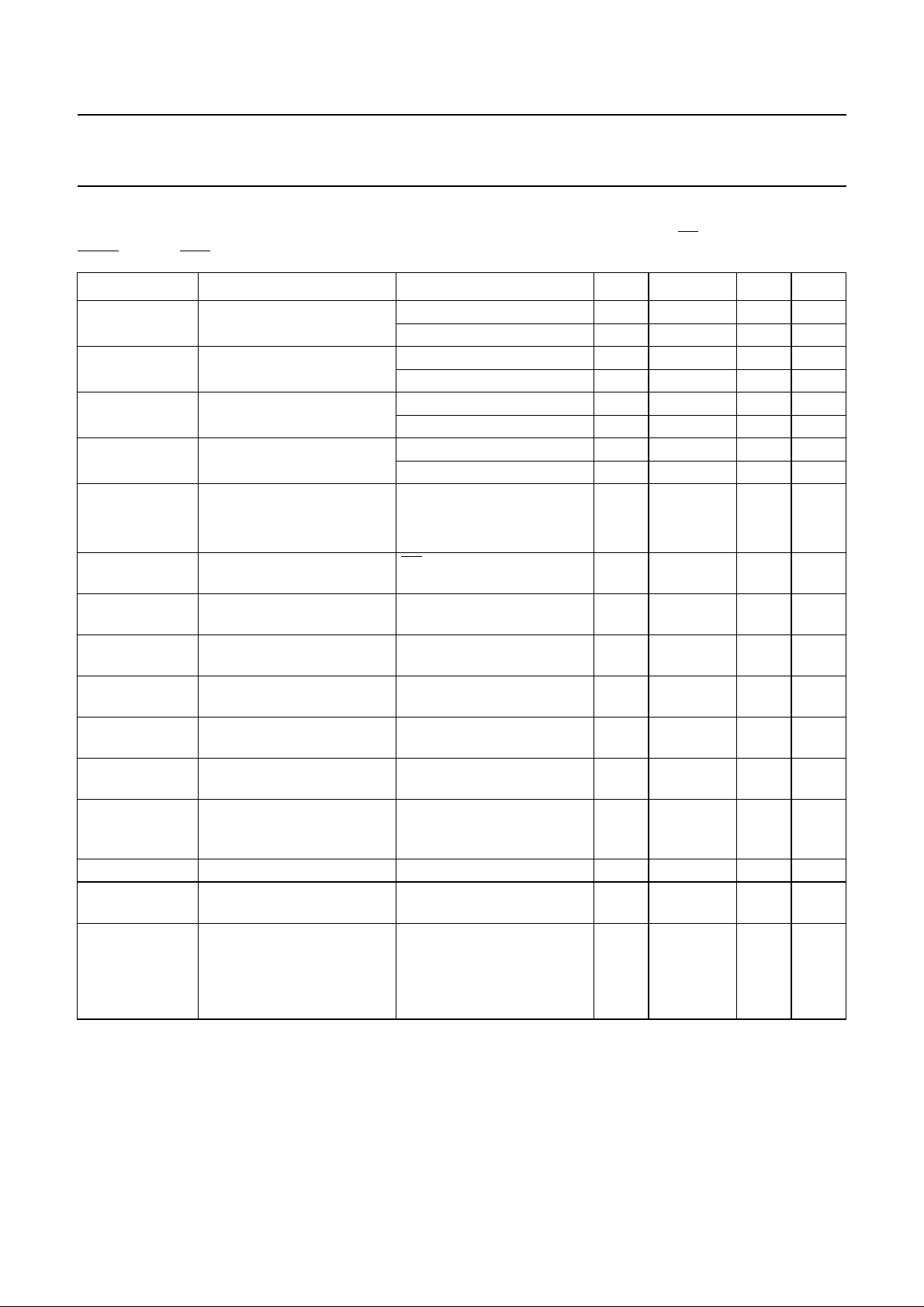
QUICK REFERENCE DATA
I
= 15 mA; R
line
MUTE = HIGH; BPC = HIGH; measured according to test circuits; unless otherwise specified.
SYMBOL PARAMETER CONDITIONS MIN. TYP. MAX. UNIT
I
line
V
SLPE
V
BB
V
DD
I
BB
I
BB(PD)
G
v(MIC-LN)
G
v(IR-RECO)
∆G
v(RECO-EARO)
G
v(TXI-TXO)
G
v(HFTX-LN)
G
v(HFRX-LSAO
SWR switching range − 40 − dB
∆SWR switching range adjustment with R
∆G
v(trx)
SLPE
=20Ω;Z
= 600 Ω; f = 1 kHz;T
line
=25°C; AGCpin connected to LN; PD = HIGH;HFC = LOW;
amb
line current operating range normal operation 11 − 130 mA
with reduced performance 1 − 11 mA
stabilized voltage between
SLPE and GND
regulated supply voltage for
internal circuitry
regulated supply voltage on
pin V
DD
current available on pin V
I
= 15 mA 3.4 3.7 4.0 V
line
I
= 70 mA 5.7 6.1 6.5 V
line
I
= 15 mA 2.75 3.0 3.25 V
line
I
= 70 mA 4.9 5.3 5.7 V
line
VBB> 3.35 V + 0.25 V (typ.) 3.1 3.35 3.6 V
otherwise − V
BB
− 0.25 − V
BB
in speech mode − 11 − mA
in handsfree mode − 9 − mA
current consumption on V
PD = LOW − 460 −µA
BB
during power-down phase
voltage gain from pin
V
= 5 mV (RMS) 43.3 44.3 45.3 dB
MIC
MIC+/MIC− to LN
voltage gain from pin IR
(referenced to LN) to RECO
gain voltage range between
VIR= 15 mV (RMS);
HFC = HIGH
28.7 29.7 30.7 dB
−3 − +15 dB
pins RECO and EARO
voltage gain from pin TXI to
TXO
voltage gain from pin HFTX
V
= 3 mV (RMS);
TXI
R
= 30.1 kΩ
GATX
V
= 15 mV (RMS) 33.5 34.7 35.9 dB
HFTX
12.7 15.2 17.7 dB
to LN
) voltage gain from pin HFRX
to LSAO
V
= 30 mV (RMS);
HFRX
R
= 255 kΩ;
GALS
I
=70mA
line
SWR
referenced to
25.5 28 30.5 dB
−40 − +12 dB
365 kΩ
gain control range for
I
= 70 mA 5.45 6.45 7.45 dB
line
transmit and receive
amplifiers affected by the
AGC; with respect to
I
=15mA
line
2000 Mar 21 3
Philips Semiconductors Preliminary specification
Speech and handsfree IC TEA1098A
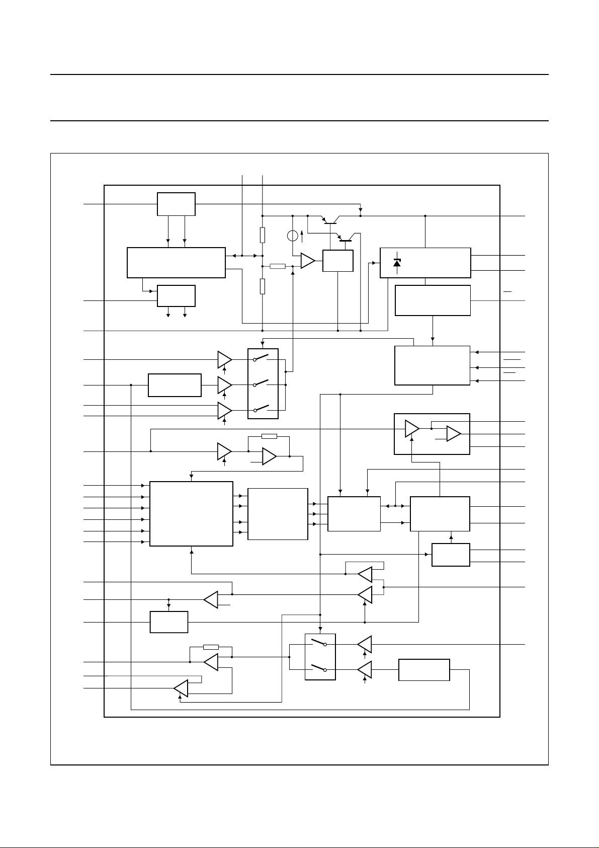
BLOCK DIAGRAM
REG
handbook, full pagewidth
LN 19 (15)
STARTER
LINE CURRENT DETECTION
LOW VOLTAGE BEHAVIOUR
SLPE
20
(16)18(14)
R1
SWITCH
SUPPLY
MANAGEMENT
(10) 14
(19) 23
(20) 24
V
BB
V
DD
MICS
AGC
GND
HFTX
DTMF
MIC+
MIC−
TXI
TSEN
TENV
TNOI
RNOI
RENV
RSEN
GALS
LSAO
22 (18)
17 (13)
39 (36)
35 (32)
34 (31)
33 (30)
31 (28)
9 (4)
8 (3)
7 (2)
10 (5)
12 (7)
11 (6)
15 (11)
16 (12)
AGC
tail currents for preamps
ATTENUATOR
TX AND RX
ENVELOPE AND NOISE
DETECTORS
BUFFERS
AND
COMPARATORS
TEA1098A
DUCO LOGIC
SWT STATUS
POWER-DOWN
CURRENT SOURCES
LOGIC
INPUTS
DECODING
VOICE
SWITCH
VOLUME
CONTROL
(38) 1
(37) 40
(39) 2
(40) 3
(27) 30
(26) 29
(29) 32
(24) 27
(25) 28
(21) 25
(22) 26
(41) 4
(42) 5
(1) 6
PD
HFC
MUTE
BPC
GATX
TXO
GNDTX
SWT
IDT
STAB
SWR
EVCI
LVCI
HFRX
13 (8)
DLC
RECO
GARX
EARO
38 (35)
37 (34)
36 (33)
DYNAMIC
LIMITER
Fig.1 Block diagram.
2000 Mar 21 4
ATTENUATOR
(17) 21
FCA140
IR
Philips Semiconductors Preliminary specification
Speech and handsfree IC TEA1098A
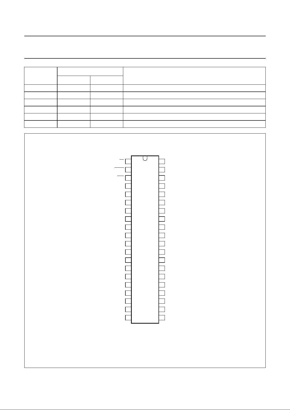
PINNING
SYMBOL
PD 1 38 power-down input (active LOW)
MUTE 2 39 logic input (active LOW)
BPC 3 40 logic input (active LOW)
EVCI 4 41 logic input for digital volume control (earpiece and loudspeaker LSB)
LVCI 5 42 logic input for digital volume control (loudspeaker MSB)
n.c. − 43 not connected
n.c. − 44 not connected
HFRX 6 1 receive input for loudspeaker amplifier
TNOI 7 2 transmit noise envelope timing adjustment
TENV 8 3 transmit signal envelope timing adjustment
TSEN 9 4 transmit signal envelope sensitivity adjustment
RNOI 10 5 receive noise envelope timing adjustment
RSEN 11 6 receive signal envelope sensitivity adjustment
RENV 12 7 receive signal envelope timing adjustment
DLC 13 8 dynamic limiter capacitor for the loudspeaker amplifier
n.c. − 9 not connected
V
BB
GALS 15 11 loudspeaker amplifier gain adjustment
LSAO 16 12 loudspeaker amplifier output
GND 17 13 ground reference
SLPE 18 14 line current sense
LN 19 15 positive line terminal
REG 20 16 line voltage regulator decoupling
IR 21 17 receive amplifier input
AGC 22 18 automatic gain control/line loss compensation
V
DD
MICS 24 20 microphone supply
STAB 25 21 reference current adjustment
SWR 26 22 switching range adjustment
n.c. − 23 not connected
SWT 27 24 switch-over timing adjustment
IDT 28 25 Idle mode timing adjustment
TXO 29 26 handsfree microphone amplifier output
GATX 30 27 handsfree microphone amplifier gain adjustment
TXI 31 28 handsfree microphone amplifier input
GNDTX 32 29 ground reference for microphone amplifiers
MIC− 33 30 negative handset microphone amplifier input
MIC+ 34 31 positive handset microphone amplifier input
TEA1098ATV TEA1098AH
14 10 stabilized supply for internal circuitry
23 19 3.35 V regulated voltage supply for microcontrollers
PIN
DESCRIPTION
2000 Mar 21 5
Philips Semiconductors Preliminary specification
Speech and handsfree IC TEA1098A
SYMBOL
DESCRIPTION
TEA1098ATV TEA1098AH
DTMF 35 32 dual tone multi-frequency input
EARO 36 33 earpiece amplifier output
GARX 37 34 earpiece amplifier gain adjustment
RECO 38 35 receive amplifier output
HFTX 39 36 transmit input for line amplifier
HFC 40 37 logic input
PIN
handbook, halfpage
PD
MUTE
BPC
EVCI
LVCI
HFRX
TNOI
TENV
TSEN
RNOI
RSEN
RENV
DLC
V
BB
GALS
LSAO
GND
SLPE
LN
REG
1
2
3
4
5
6
7
8
9
10
TEA1098ATV
11
12
13
14
15
16
17
18
19
20
FCA141
40
39
38
37
36
35
34
33
32
31
30
29
28
27
26
25
24
23
22
21
HFC
HFTX
RECO
GARX
EARO
DTMF
MIC+
MIC−
GNDTX
TXI
GATX
TXO
IDT
SWT
SWR
STAB
MICS
V
DD
AGC
IR
Fig.2 Pin configuration (TEA1098ATV).
2000 Mar 21 6

Philips Semiconductors Preliminary specification
Speech and handsfree IC TEA1098A
handbook, full pagewidth
n.c.
LVCI
EVCI
BPC
MUTE
PD
HFTX
RECO
n.c.
44
HFC
43
42
41
40
39
38
37
GARX
36
35
34
1
HFRX
2
TNOI
3
TENV
4
TSEN
5
RNOI
6
RSEN
RENV
7
DLC
8
n.c.
9
V
10
BB
GALS
11
12
13
14
15
LN
GND
SLPE
LSAO
Fig.3 Pin configuration (TEA1098AH).
FUNCTIONAL DESCRIPTION
All data given in this chapter are typical values, except
when otherwise specified.
Supplies
TEA1098AH
16
17
REGIRAGC
This capacitor converted into an equivalent inductance
realizes the set impedance conversion from its DC value
(R
The IC regulates the line voltage at pin LN and can be
calculated as follows:
33
EARO
DTMF
32
31
MIC+
30
MIC−
GNDTX
29
28
TXI
GATX
27
TXO
26
IDT
25
24
SWT
n.c.
23
21
22
20
18
19
DD
V
MICS
STAB
) to its AC value (done by an external impedance).
SLPE
FCA142
SWR
LINE INTERFACE AND INTERNAL SUPPLY (PINS LN, SLPE,
REG AND VBB)
The supply for the TEA1098A and its peripherals is
obtained from the line. The IC generates a stabilized
reference voltage (V
) between pins SLPE and GND.
ref
This reference voltage is equal to 3.7 V for line currents
lower than 18 mA. It than increases linearly with the line
current and reaches the value of 6.1 V for line currents
higher than 45 mA. For line currents below 9 mA, the
internal reference voltage generating V
is automatically
ref
adjusted to a lowervalue. This is the so-calledlow voltage
area and the TEA1098A has limited performances in this
area (see Section “Low voltage behaviour”). This
reference voltage is temperature compensated.
The voltage between pins SLPE and REG is used by the
internal regulator to generate the stabilized reference
voltageand is decoupledby means ofacapacitor between
pins LN and REG.
2000 Mar 21 7
V
I
V
=
LN
SLPEIline
refRSLPE
I×+
SLPE
Ix–=
where:
I
= line current
line
Ix= current consumed on pin LN (approximately a few µA)
I
= current flowing through the R
SLPE
The preferred value for R
is 20 Ω. Changing this value
SLPE
SLPE
resistor
will affect more than the DC characteristics; it also
influences the transmit gains to the line, the gain control
characteristic, thesidetone level and the maximum output
swing on the line.
Philips Semiconductors Preliminary specification
Speech and handsfree IC TEA1098A
handbook, full pagewidth
LN
REG
GND
C
REG
4.7 µF
SLPE
TP1
R3
R2
TN1
R1
from
preamp
R
SLPE
20 Ω
J1
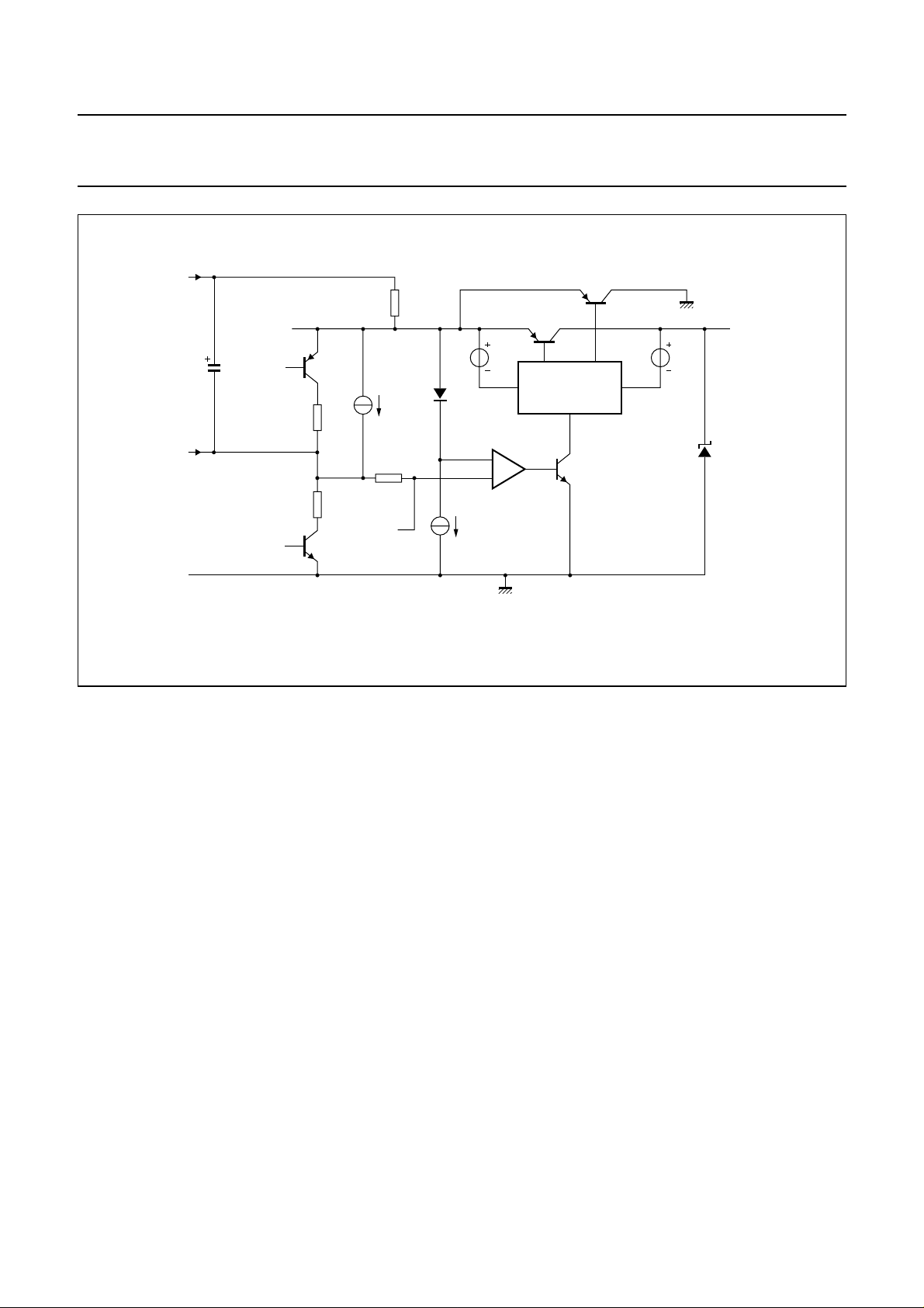
Fig.4 Line interface principle.
As can beseen fromFig.4, theinternal circuitryis supplied
by pin VBB, which is a strong supply point combined with
the line interface. The line current is flowing through the
R
resistor and is sunk by the VBB voltage stabilizer,
SLPE
thusbecoming availablefor a loudspeakeramplifier orany
peripheral IC. Its voltage is equal to 3.0 V for line currents
lower than 18 mA. It than increases linearly with the line
current and reaches the value of 5.3 V for line currents
greater than 45 mA. It is temperature compensated.
TR2
GND
TR1
E1
D1
J2
GND
Thereference voltageV
TN2
E2
MGM298
canbe increasedbyconnecting
ref
D1
V
BB
an external resistor between pins REG and SLPE. For
large line currents, this increase can slightly affect some
dynamic performances such as maximum signal level on
the line for 2% THD. The voltage on pin VBBis not affected
by this external resistor; see Fig.5 for the main DC
voltages.
The aim of the current switch TR1 and TR2 is to reduce
distortionof largeAC line signals.Current I
SLPE
issupplied
to VBBvia TR1 when the voltage on SLPE is greater than
VBB+ 0.25 V.When thevoltageon SLPE islower than this
value, the current I
is shunted to GND via TR2.
SLPE
2000 Mar 21 8

Philips Semiconductors Preliminary specification
Speech and handsfree IC TEA1098A
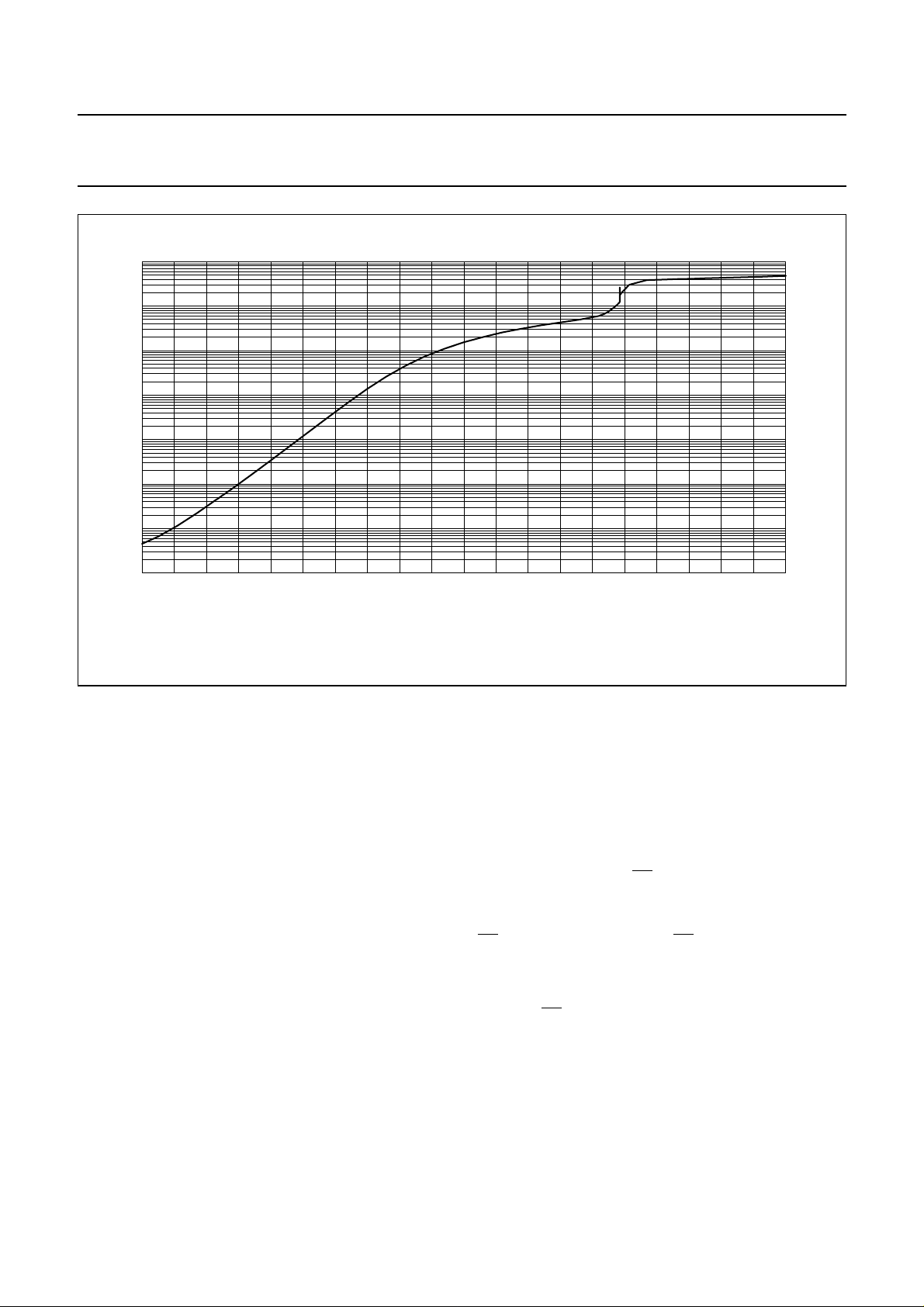
handbook, full pagewidth
8
Voltages
(V)
6
4
2
0
0.00 0.01
0.02 0.05
0.040.03
Fig.5 Main DC voltages.
MGL439
LN
SLPE
VBB
VDD
MICS
0.070.06
Line current (A)
V
SUPPLY FOR MICROCONTROLLER (PIN V
DD
Thevoltage on theV
supplypoint follows thevoltage on VBBwitha difference typicallyequal to 250 mVand is internally
DD
DD
)
limited to 3.35 V. This voltage is temperature compensated. This supplypoint can provide a current up to 3 mAtypically.
Its internal consumption stays low (a few 10 nA) as long as VDD does not exceed 1.5 V.
VDD can also be used as an input; in this case the voltage will be stabilised to 3.35 V up to 75 mA input current.
VBB and VDDcan supply external circuits in the limit of currents provided from the line, taking into account the internal
current consumption.
2000 Mar 21 9
Philips Semiconductors Preliminary specification
Speech and handsfree IC TEA1098A
100.0u
handbook, full pagewidth
I
(A)
DD
10.0u
1.0u
100.0n
10.0n
1.0n
100.0p
10.0p
1.0
MGL438
1.5 2.5 3.0
2.0
VDD (V)
Fig.6 Current consumption on VDD.
SUPPLY FOR MICROPHONE (PINS MICS AND GNDTX)
The MICS output can be used as a supply for an electret
microphone. Its voltage is equal to 2.0 V; it can source a
current up to 1 mA and has an output impedance equal to
200 Ω.
LOW VOLTAGE BEHAVIOUR
For line currents below 9 mA, the reference voltage is
automatically adjusted to a lower value; the VBB voltage
follows the SLPE voltage with 250 mV difference. The
excess current available for other purposes than DC
biasing of the IC becomes small. In this low voltage area,
the IC has limited performances.
When the VBBvoltage becomes lower than 2.7 V, the V
BB
detector of the receive dynamic limiter on pin LSAO acts
continuously, discharging the capacitor connected to
pin DLC. In the DC condition, the loudspeaker is then
automatically disabled below this voltage.
When VBBgoes below 2.5 V, the TEA1098A is forced into
a low voltage mode whatever thelevels onthe logic inputs
are. It is a speech mode with reduced performances only
enablingthe microphone channel(between the MICinputs
and LN) and the earpiece amplifier. These two channels
are able to deliver signals for line currents as small as
3 mA. The HFC input is tied to GND sinking a current
typically equal to 300 µA.
POWER-DOWN MODE (PIN PD)
To reduce consumption during dialling or register recall
(flash),the TEA1098A isprovided withapower-down input
(PD). When the voltage on pin PD is LOW, the current
consumption from VBB and VDD is reduced to 460 µA
typically. Therefore a capacitor of 470 µF on VBB is
sufficient to power the TEA1098A during pulse dialling or
flash. The PD input has a pull-up structure. In this mode,
the capacitor C
is internally disconnected.
REG
2000 Mar 21 10

Philips Semiconductors Preliminary specification
Speech and handsfree IC TEA1098A
Transmit channels (pins MIC+, MIC−, DTMF, HFTX
and LN)
HANDSET MICROPHONE AMPLIFIER (PINS MIC+, MIC−
AND LN)
The TEA1098A has symmetrical microphone inputs. The
input impedance between pinsMIC+ and MIC− is typically
70 kΩ. The voltage gainbetween pins MIC+/MIC− and LN
is set to 44.3 dB. Without limitation from the output, the
microphone input stage can accommodate signals up to
18 mV (RMS) at room temperature for 2% of Total
Harmonic Distortion (THD). The microphone inputs are
biased at one diode voltage.
Automatic gain control is provided for line loss
compensation.
DTMF AMPLIFIER (PINS DTMF, LN AND RECO)
The TEA1098A has an asymmetrical DTMF input. The
inputimpedance betweenpins DTMF andGND istypically
20 kΩ. The voltagegain betweenpins DTMF andLN isset
to 25.35 dB. Without limitation from the output, the input
stage can accommodate signals up to 180 mV (RMS) at
room temperature for 2% of THD.
When the DTMF amplifier is enabled, dialling tones may
be sent on the line. These tones can be heard in the
earpiece or in the loudspeaker ata lowlevel. This is called
theconfidence tone. Thevoltageattenuation between pins
DTMF andRECO is typically−16.5 dB in handsfreemode
(HFC HIGH), and −28.2 dB in handset mode (HFC LOW).
The DC biasing of this input is 0 V.
The automatic gain control has no effect on these
channels.
HANDSFREE TRANSMIT AMPLIFIER (PINS HFTX AND LN)
The TEA1098A has an asymmetrical HFTX input, which is
mainly intended for use in combination with the TXO
output. The input impedance between pins HFTX and
GND is typically 20 kΩ. The voltage gain between pins
HFTX andLN is set to 34.7 dB. Without limitation fromthe
output, the input stage can accommodate signals up to
95 mV (RMS) at room temperature for 2% of THD. The
HFTX input is biased at two diodes voltage.
Automatic gain control is provided for line loss
compensation.
Receive channels (pins IR, RECO, GARX, EARO
and EVCI)
RX AMPLIFIER (PINS IR, RECO AND EVCI)
The receive amplifier has one inputIR which is referred to
the line. The input impedance between pins IR and LN is
typically 20 kΩ and the DC biasing between these pins is
equal to one diode voltage.
When HFC = 0, the gain between pins IR (referred to LN)
and RECO is typically 17.0 dB which compensates
typically 15 dB lower than attenuation of the anti-sidetone
network. The receive amplifier gain can be digitally
increased with the 4-level logic input EVCI, providing
4 steps of 4.85 dB which apply in all handset receive
modes. Without limitation from the output, the input stage
can accommodate signals up to 50 mV (RMS) at room
temperature for 2% of THD.
When HFC = 1, the gain is set automatically to 29.7 dB
which compensate the anti-sidetone network attenuation
minus 2.3 dB.
Thisreceive amplifier hasarail-to-rail outputRECO,which
is designed for use with high ohmic (real) loads (larger
than 5 kΩ). This output is biased at two diodes voltage.
Automatic gain control is provided for line loss
compensation.
EARPIECE AMPLIFIER (PINS GARX AND EARO)
The earpiece amplifier is an operational amplifier having
itsoutput (EARO)and its invertinginput (GARX)available.
Its inputsignal comes, viaadecoupling capacitor,from the
receive output RECO. It is used in combination with two
resistors to get the required gain or attenuation compared
to the receive gain. The typical resistor ratio is 4, which
gives a 12 dB gain. The gain range can be chosen
between 0 dB and 20 dB.
Two external capacitors C
GAR and EARO) and C
GAR and GND) ensure stability. The C
(connected between pins
GAR
(connected between pins
GARS
capacitor
GAR
provides a first-order low-pass filter. The cut-offfrequency
corresponds to the time constant C
relationship C
GARS
>=10×C
GAR
× RE2. The
GAR
must be fulfilled.
The earpiece amplifier has a rail-to-rail output EARO,
biasedat two diodesvoltage.It is designedforuse with low
ohmic (real) loads (150 Ω) or capacitive loads (100 nF in
series with 100 Ω).
2000 Mar 21 11
Philips Semiconductors Preliminary specification
Speech and handsfree IC TEA1098A
AGC (pin AGC)
The TEA1098A performs automatic line loss
compensation,which fits wellwiththe trueline attenuation.
The automatic gain control varies the gain of some
transmit and receive amplifiers in accordance with the DC
linecurrent. Thecontrolrange is6.45 dBfor G
G
v(IR-RECO)
and 6.8 dB for G
v(HFTX-LN)
, which corresponds
v(MIC-LN)
and
approximately to a line length of 5.5 km for a 0.5 mm
twisted-pair copper cable.
To enable this gain control, pin AGC must be shorted to
pin LN. The start currentfor compensationcorresponds to
a line current of typically 23 mA and the stop current to
57 mA. The start current can be increased by connecting
an external resistor between pins AGC and LN. It can be
increased up to 40 mA (using a resistor typically 80 kΩ).
The start and stop current will be maintained in a ratio
equal to 2.5. By leavingthe AGC pin open-circuit, thegain
control is disabled and no line loss compensation is
performed.
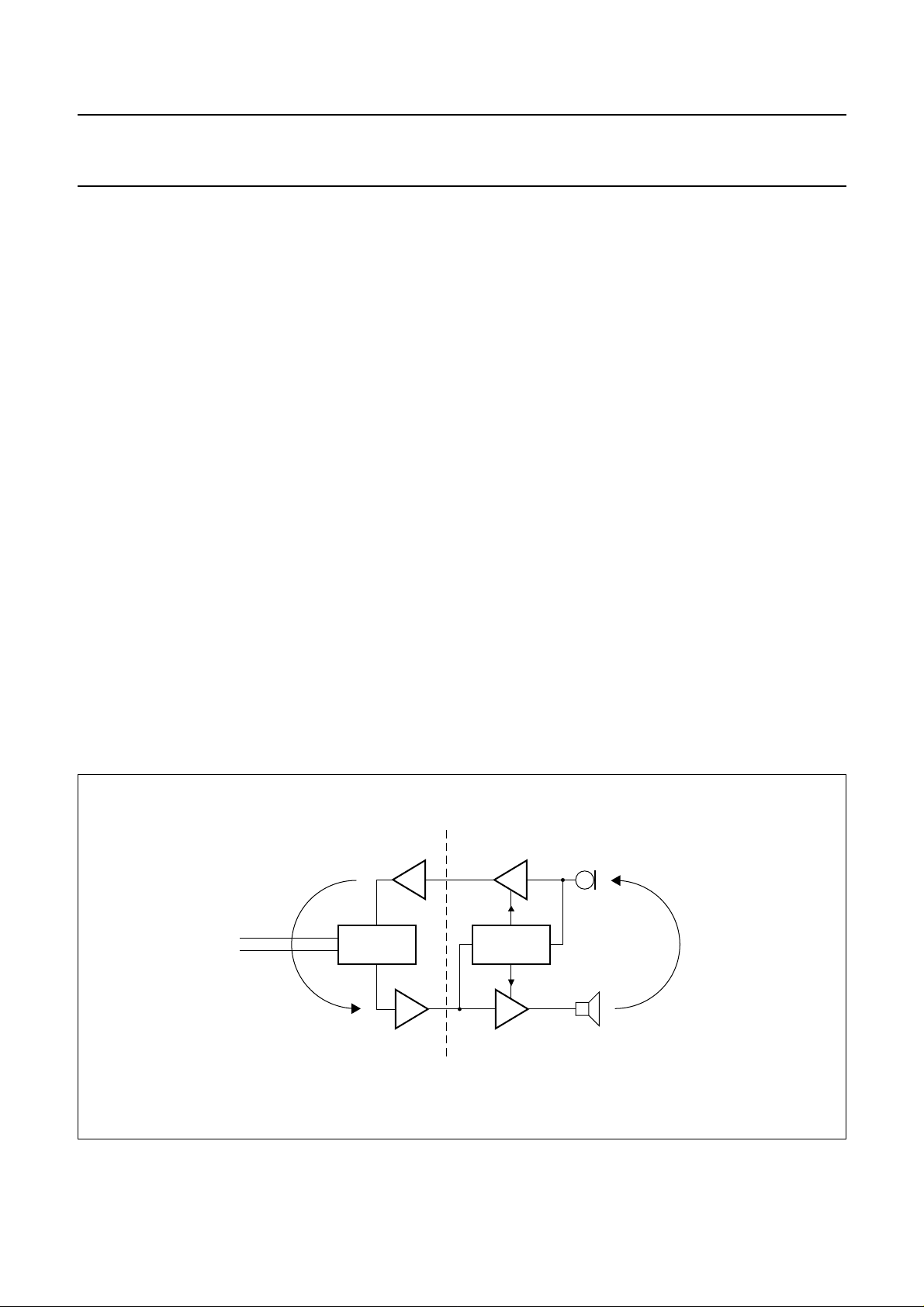
Handsfree application
As can be seen from Fig.4, a loop is formed via the
sidetone network in the line interface part and the acoustic
coupling between loudspeaker and microphone of the
handsfree part. When this loop gain is greater than 1,
howling occurs. In a full duplex application this would be
the case. The loop-gain has to be much lower than 1 and
therefore has to be decreased to avoid howling.
This is achieved by the duplex controller. The duplex
controller of the TEA1098Adetects whichchannel has the
‘largest’ signal and then controls the gains of the
microphone and loudspeaker amplifiersso thatthe sum of
the gains remains constant.
As a result, in handsfree application, the circuit can be in
three stable modes:
1. Transmit mode (TX mode).
Thegain ofthemicrophone amplifier isat its maximum
and the gain of the loudspeaker amplifier is at its
minimum.
2. Receive mode (RX mode).
The gain of the loudspeaker amplifier is at its
maximum and the gain of the microphone amplifier is
at its minimum.
3. Idle mode.
The gain of the amplifiers is halfway between their
maximum and minimum value.
The difference between the maximum gain and minimum
gain is called the switching range.
handbook, full pagewidth
telephone
line
sidetone
HYBRID
Fig.7 Handsfree telephone set principles.
2000 Mar 21 12
acoustic
coupling
DUPLEX
CONTROL
MGM299
 Loading...