

Philips TEA1097TV, TEA1097H Datasheet

INTEGRATED CIRCUITS
DATA SH EET
TEA1097
Speech and loudspeaker amplifier
IC with auxiliary inputs/outputs and
analog multiplexer
Product specification
Supersedes data of 1998 Jun 11
File under Integrated Circuits, IC03
1999 Apr 08

Philips Semiconductors Product specification
Speech and loudspeaker amplifier IC with
auxiliary inputs/outputs and analog multiplexer
FEATURES
Line interface
• Low DC line voltage
• Voltage regulator with adjustable DC voltage
• Symmetrical high-impedance inputs (70 kΩ) for
dynamic, magnetic or electric microphones
• Dual Tone Multi-Frequency (DTMF) input with
confidence tone on earphone and/or loudspeaker
• Receive amplifier for dynamic, magnetic or
piezo-electric earpieces (with externally adjustable gain)
• Automatic Gain Control (AGC) for true line loss
compensation.
Supplies
• Provides a strong 3.35 V regulated supply for
microcontroller or dialler
• Provides filtered power supply, optimized according to
line current and compatible with external voltage or
current sources
• Filtered 2 V power supply output for electret microphone
• Compatible with a ringer mode
• Power-Down (
Loudspeaker amplifier
• Single-ended rail-to-rail output
• Externally adjustable gain
• Dynamic limiter to prevent distortion
• Logarithmic volume control via linear potentiometer.
Auxiliary interfaces
• Asymmetrical high-impedance input for electret
microphone.
PD) logic input for power-down.
• General purpose auxiliary output for transmit and
receive
• Auxiliary transmit input with high signal level capability
dedicated to line transmission
• Auxiliary receive input with high signal level capability
• Integrated multiplexer for channels selection.
APPLICATIONS
• Telephone answering machines
• Telephones with digital handsfree
• Line powered telephone sets
• Cordless telephones
• Fax machines.
GENERAL DESCRIPTION
The TEA1097 is an analog bipolar circuit dedicated for
telephone applications. It includes a line interface, handset
microphone and earpiece amplifiers, base microphone
and loudspeaker amplifiers, some specific auxiliary
Inputs/Outputs (I/Os) and an analog multiplexer to enable
the right transmit and/or receive channels. The multiplexer
is controlled by a logic circuitry decoding four logic inputs
provided by a microcontroller. Twelve different application
modes have been defined and can be accessed by
selecting the right logic inputs.
This IC can be supplied by the line and/or by the mains if
available (in a cordless telephone or a telephone
answering machine for example). It provides a 3.35 V
supply for a microcontroller or dialler and a 2 V filtered
voltage supply for electret microphones. The IC is
designed to facilitate the use of the loudspeaker amplifier
during ringing phase.
TEA1097
ORDERING INFORMATION
TYPE
NUMBER
TEA1097TV VSO40 plastic very small outline package; 40 leads SOT158-1
TEA1097H QFP44 plastic quad flat package; 44 leads (lead length 1.3 mm);
1999 Apr 08 2
NAME DESCRIPTION VERSION
body 10 × 10 × 1.75 mm
PACKAGE
SOT307-2
Philips Semiconductors Product specification
Speech and loudspeaker amplifier IC with
TEA1097
auxiliary inputs/outputs and analog multiplexer
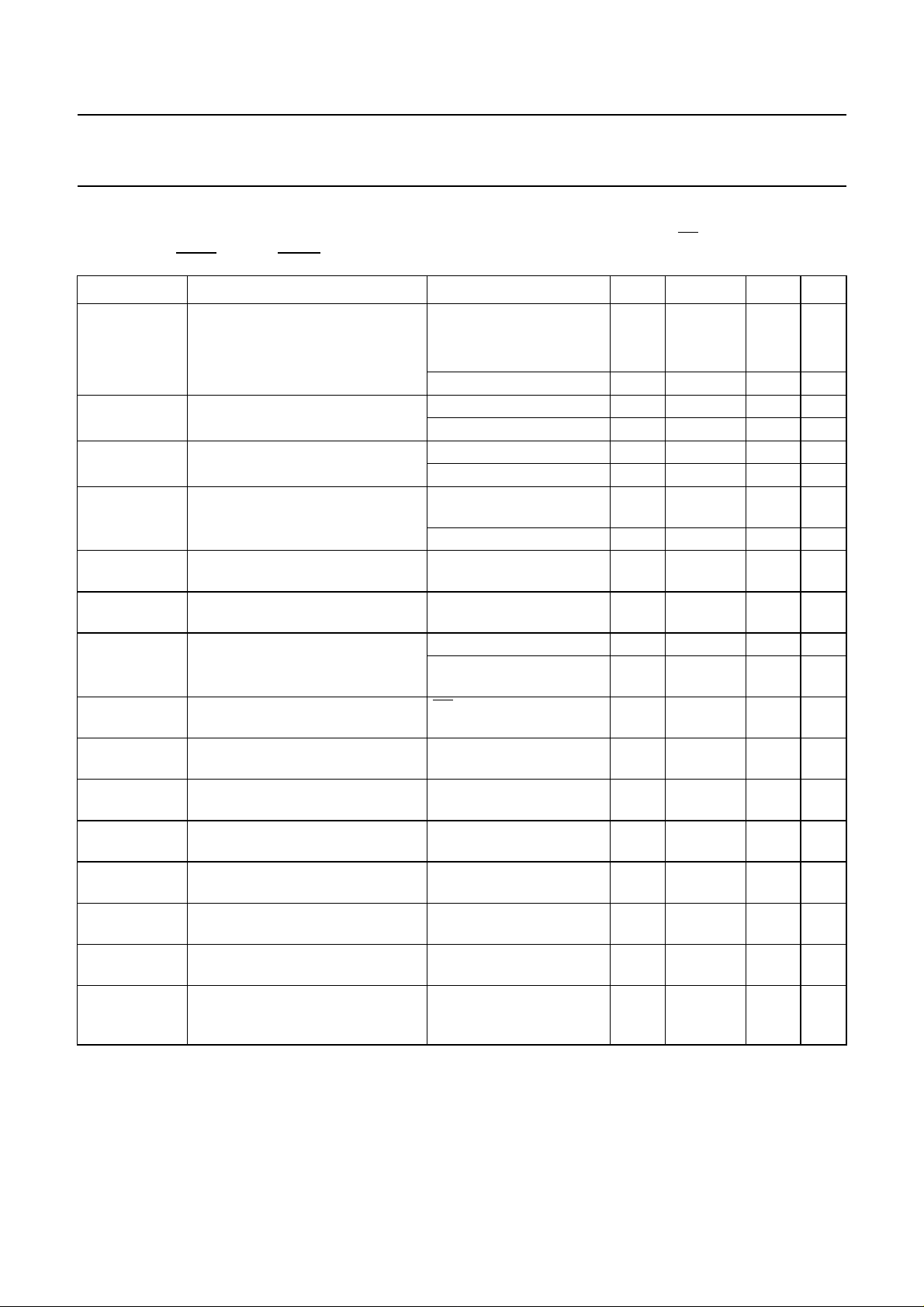
QUICK REFERENCE DATA
I
= 15 mA; R
line
AUXC = LOW;
SYMBOL PARAMETER CONDITIONS MIN. TYP. MAX. UNIT
I
line
V
SLPE
V
BB
V
DD
V
ESI(ext)
I
ESI(ext)
I
BB
I
BB(pd)
G
v(MIC-LN)
G
v(IR-RECO)
∆G
v(QR)
G
v(TXIN-TXOUT)
G
v(TXAUX-LN)
G
v(HFRX-LSAO)
∆G
v(trx)
SLPE
=20Ω; Z
= 600 Ω; f = 1 kHz; T
line
=25°C; AGC pin connected to LN;PD = HIGH; HFC = LOW;
amb
MUTT = HIGH; MUTR = HIGH; measured according to test circuits; unless otherwise specified.
line current operating range normal operation
TEA1097H 11 − 140 mA
TEA1097TV 11 − 130 mA
with reduced performance 1 − 11 mA
stabilized voltage between SLPE
and GND (V
ref
)
regulated supply voltage for
internal circuitry
regulated supply voltage on
pin V
DD
external voltage supply allowed on
I
= 15 mA 3.4 3.7 4.0 V
line
I
= 70 mA 5.7 6.1 6.5 V
line
I
= 15 mA 2.75 3.0 3.25 V
line
I
= 70 mA 4.9 5.3 5.7 V
line
VBB> 3.35 V + 0.25 V
3.1 3.35 3.6 V
(typ.)
otherwise − V
− 0.25 − V
BB
−− 6V
pin ESI
external current supply allowed on
−− 140 mA
pin ESI
current available on pin V
BB
speech mode − 11 − mA
handsfree mode;
− 9.5 − mA
HFC = HIGH
current consumption on VBB during
PD = LOW − 460 −µA
power-down phase
voltage gain from pin
V
= 5 mV (RMS) 43.3 44.3 45.3 dB
MIC
MIC+/MIC− to LN
voltage gain from pin IR
VIR= 15 mV (RMS) 28.7 29.7 30.7 dB
(referenced to LN) to RECO
gain voltage range between pins
−3 − +15 dB
RECO and QR
voltage gain from pin TXIN to
TXOUT
voltage gain from pin TXAUX to LN V
V
= 3 mV (RMS);
TXIN
R
= 30.1 kΩ; note 1
GATX
= 0.1 V (RMS);
TXAUX
13.15 14.85 16.55 dB
11.5 12.5 13.5 dB
note 1
voltage gain from pin HFRX to
LSAO
gain control range for transmit and
receive amplifiers affected by the
AGC; with respect to I
=15mA
line
V
= 20 mV (RMS);
HFRX
R
= 255 kΩ; note 1
GALS
I
= 70 mA; on
line
G
v(MIC-LN)
and G
v(IR-AUXO)
, G
v(IR-RECO)
25.5 28 30.5 dB
5.45 6.45 7.45 dB
Note
1. When the channel is enabled according to Table 1.
1999 Apr 08 3
Philips Semiconductors Product specification
Speech and loudspeaker amplifier IC with
auxiliary inputs/outputs and analog multiplexer
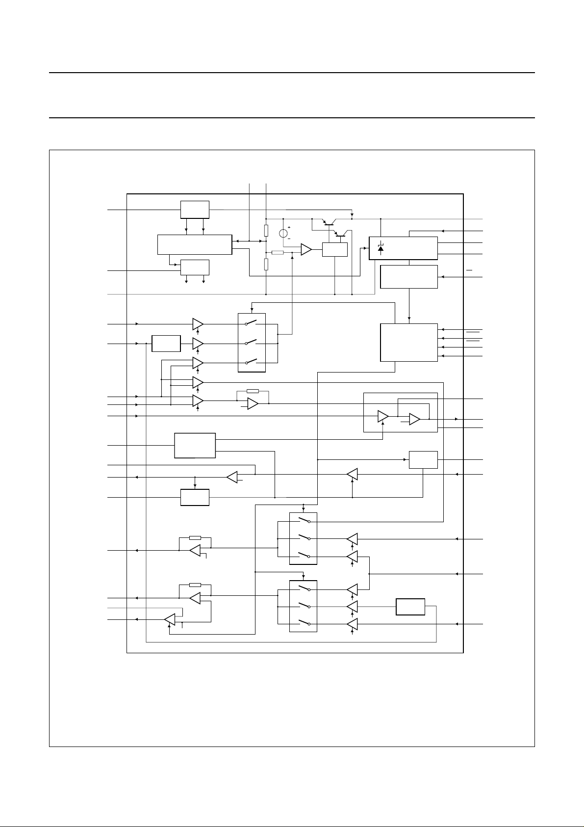
BLOCK DIAGRAM
handbook, full pagewidth
REG SLPE
20
(16)18(14)
AGC
GND
TXAUX
DTMF
19 (15)
LN
22 (18)
17 (13)
5 (43)
34 (32)
STARTER
LINE CURRENT DETECTION
LOW VOLTAGE BEHAVIOUR
AGC
Tail currents for preamps
ATT.
SWITCH
TEA1097TV
SUPPLY
D6
MANAGEMENT
POWER-DOWN
CURRENT SOURCES
ANALOG
MULTIPLEXER
CONTROL
TEA1097
V
(10) 13
BB
(9) 12
ESI
V
(19) 23
DD
(20) 24
MICS
(38) 40
PD
HFC(37) 39
MUTT(39) 1
MUTR(40) 2
AUXC(41) 3
33 (31)
MIC+
32 (30)
MIC−
30 (28)
TXIN
STAB 25 (21)
GALS 14 (11)
16 (12)
LSAO
DLC 11 (8)
6 (44)
AUXO
37 (35)
RECO
36 (34)
GARX
35 (33)
QR
TAIL
CURRENTS
DYNAMIC
LIMITER
VOLUME
CONTROL
ATT.
(26) 28
(1) 7
(36) 38
(17) 21
(42) 4
MGL392
GATX(27) 29
TXOUT
GNDTX(29) 31
VOL(23) 27
HFRX
HFTX
IR
RAUX
The pin numbers given in parenthesis refer to the TEA1097H.
Fig.1 Block diagram.
1999 Apr 08 4
Philips Semiconductors Product specification
Speech and loudspeaker amplifier IC with
auxiliary inputs/outputs and analog multiplexer
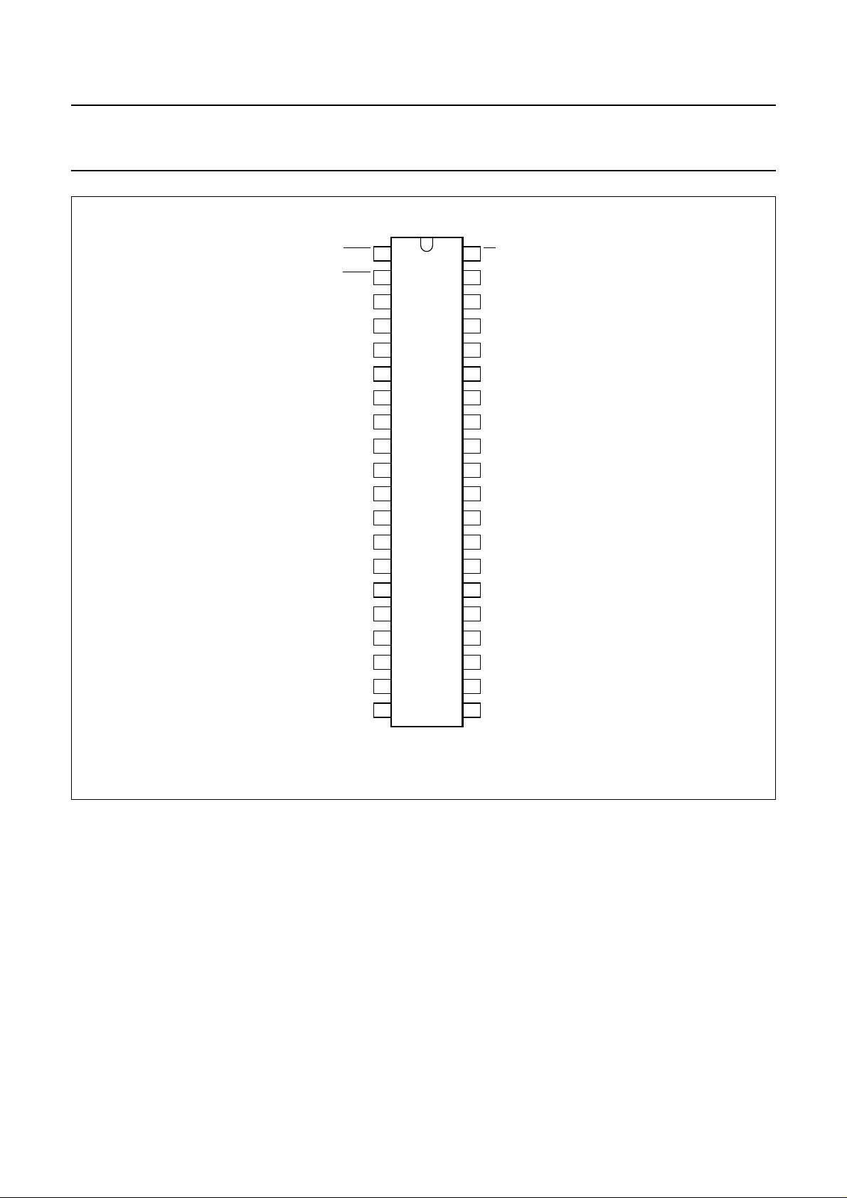
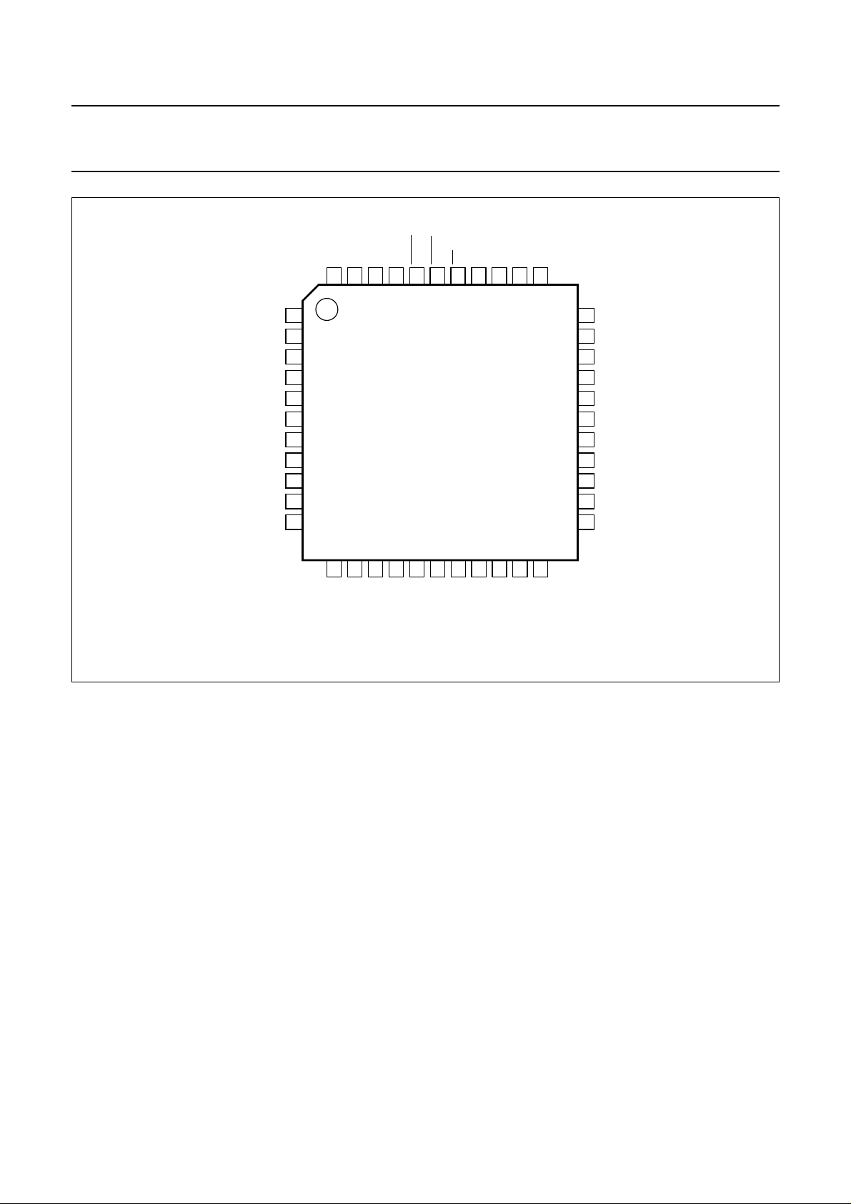
PINNING
SYMBOL
MUTT 1 39 logic input (active LOW)
MUTR 2 40 logic input (active LOW)
AUXC 3 41 logic input
RAUX 4 42 auxiliary receive amplifier input
TXAUX 5 43 auxiliary transmit amplifier input
AUXO 6 44 auxiliary amplifier output
HFRX 7 1 receive input for loudspeaker amplifier
n.c. 8 to 10,
DLC 11 8 dynamic limiter capacitor for the loudspeaker amplifier
ESI 12 9 external supply input
V
BB
GALS 14 11 loudspeaker amplifier gain adjustment
LSAO 16 12 loudspeaker amplifier output
GND 17 13 ground reference
SLPE 18 14 line current sense
LN 19 15 positive line terminal
REG 20 16 line voltage regulator decoupling
IR 21 17 receive amplifier input
AGC 22 18 automatic gain control/line loss compensation
V
DD
MICS 24 20 microphone supply output
STAB 25 21 reference current adjustment
VOL 27 23 loudspeaker volume adjustment
TXOUT 28 26 base microphone amplifier output
GATX 29 27 base microphone amplifier gain adjustment
TXIN 30 28 base microphone amplifier input
GNDTX 31 29 ground reference for microphone amplifiers
MIC− 32 30 negative handset microphone amplifier input
MIC+ 33 31 positive handset microphone amplifier input
DTMF 34 32 dual tone multi-frequency input
QR 35 33 earpiece amplifier output
GARX 36 34 earpiece amplifier gain adjustment
RECO 37 35 receive amplifier output
HFTX 38 36 transmit input for auxiliary receive amplifier
HFC 39 37 logic input
PD 40 38 power-down input (active LOW)
VSO40 QFP44
15 and 26
PIN
2 to 7, 22,
24 and 25
13 10 stabilized supply for internal circuitry
23 19 3.35 V regulated voltage supply for microcontroller
not connected
DESCRIPTION
TEA1097
1999 Apr 08 5
Philips Semiconductors Product specification
Speech and loudspeaker amplifier IC with
auxiliary inputs/outputs and analog multiplexer
handbook, halfpage
MUTT
MUTR
AUXC
RAUX
TXAUX
AUXO
HFRX
n.c.
n.c.
n.c.
DLC
ESI
V
BB
GALS
n.c.
LSAO
GND
SLPE
LN
REG
1
2
3
4
5
6
7
8
9
10
TEA1097TV
11
12
13
14
15
16
17
18
19
20
MGL393
40
39
38
37
36
35
34
33
32
31
30
29
28
27
26
25
24
23
22
21
PD
HFC
HFTX
RECO
GARX
QR
DTMF
MIC+
MIC−
GNDTX
TXIN
GATX
TXOUT
VOL
n.c.
STAB
MICS
V
AGC
IR
TEA1097
DD
Fig.2 Pin configuration (VSO40).
1999 Apr 08 6
Philips Semiconductors Product specification
Speech and loudspeaker amplifier IC with
auxiliary inputs/outputs and analog multiplexer
handbook, full pagewidth
HFRX
n.c.
n.c.
n.c
n.c
n.c
n.c
DLC
ESI
V
BB
GALS
TXAUX
43
RAUX
42
AUXC
41
TEA1097H
AUXO
44
1
2
3
4
5
6
7
8
9
10
11
MUTR
40
MUTT
39
PD
38
HFC
37
HFTX
36
RECO
35
GARX
34
33
32
31
30
29
28
27
26
25
24
23
TEA1097
QR
DTMF
MIC+
MIC−
GNDTX
TXIN
GATX
TXOUT
n.c.
n.c.
VOL
12
13
14
15
LN
GND
SLPE
LSAO
Fig.3 Pin configuration (QFP44).
FUNCTIONAL DESCRIPTION
All data given in this chapter are typical values, except
when otherwise specified.
Supplies
L
INE INTERFACE AND INTERNAL SUPPLY (PINS LN, SLPE,
REG
AND V
BB
)
The supply for the TEA1097 and its peripherals is obtained
from the line. The IC generates a stabilized reference
voltage (V
) between pins SLPE and GND. This
ref
reference voltage is equal to 3.7 V for line currents lower
than 18 mA. It than increases linearly with the line current
and reaches the value of 6.1 V for line currents higher than
45 mA. For line currents below 9 mA, the internal
reference voltage generating V
is automatically adjusted
ref
to a lower value. This is the so-called low voltage area and
the TEA1097 has limited performances in this area
(see Section “Low voltage behaviour”). This reference
voltage is temperature compensated.
21
16
REG
17
18
19
IR
DD
V
AGC
20
MICS
STAB
22
n.c
FCA019
The voltage between pins SLPE and REG is used by the
internal regulator to generate the stabilized reference
voltage and is decoupled by means of a capacitor between
pins LN and REG.
This capacitor converted into an equivalent inductance
realizes the set impedance conversion from its DC value
) to its AC value (done by an external impedance).
(R
SLPE
The IC regulates the line voltage at pin LN and it can be
calculated as follows:
V
I
V
=
LN
SLPEIline
refRSLPE
I×+
SLPE
Ix–=
where:
I
= line current
line
Ix= current consumed on pin LN (approximately a
few µA)
I
= current flowing through the R
SLPE
SLPE
resistor.
1999 Apr 08 7
Philips Semiconductors Product specification
Speech and loudspeaker amplifier IC with
auxiliary inputs/outputs and analog multiplexer
The preferred value for R
will affect more than the DC characteristics; it also
influences the transmit gains to the line, the gain control
characteristic, the sidetone level and the maximum output
swing on the line.
As can be seen from Fig.4, the internal circuitry is supplied
by pin VBB, which is a strong supply point combined with
the line interface. The line current is flowing through the
R
resistor and is sunk by the VBB voltage stabilizer,
SLPE
becoming available for a loudspeaker amplifier or any
peripheral IC. Its voltage is equal to 3.0 V for line currents
lower than 18 mA. It than increases linearly with the line
current and reaches the value of 5.3 V for line currents
greater than 45 mA. It is temperature compensated.
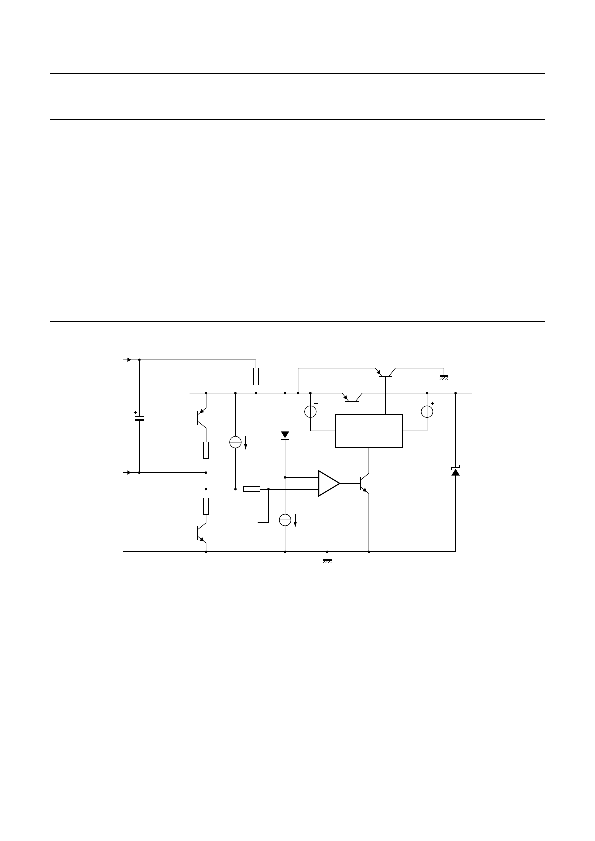
handbook, full pagewidth
LN
is 20 Ω. Changing this value
SLPE
SLPE
R
SLPE
20 Ω
The aim of the current switch TR1 and TR2 is to reduce
distortion of large AC line signals. Current I
to VBB via TR1 when the voltage on SLPE is greater than
VBB+ 0.25 V. When the voltage on SLPE is lower than this
value, the current I
The reference voltage V
an external resistor between pins REG and SLPE.
For large line currents, this increase can slightly affect
some dynamic performances such as maximum signal
level on the line for 2% THD. The voltage on pin VBB is not
affected by this external resistor. See Fig.5 for the main
DC voltages.
TR1
is shunted to GND via TR2.
SLPE
can be increased by connecting
ref
TR2
GND
TEA1097
is supplied
SLPE
V
BB
REG
GND
C
REG
4.7 µF
TP1
D1
R3
R2
TN1
R1
from
preamp
J1
Fig.4 Line interface principle.
E1
TN2
J2
GND
E2
D1
MGM298
1999 Apr 08 8
Philips Semiconductors Product specification
Speech and loudspeaker amplifier IC with
auxiliary inputs/outputs and analog multiplexer
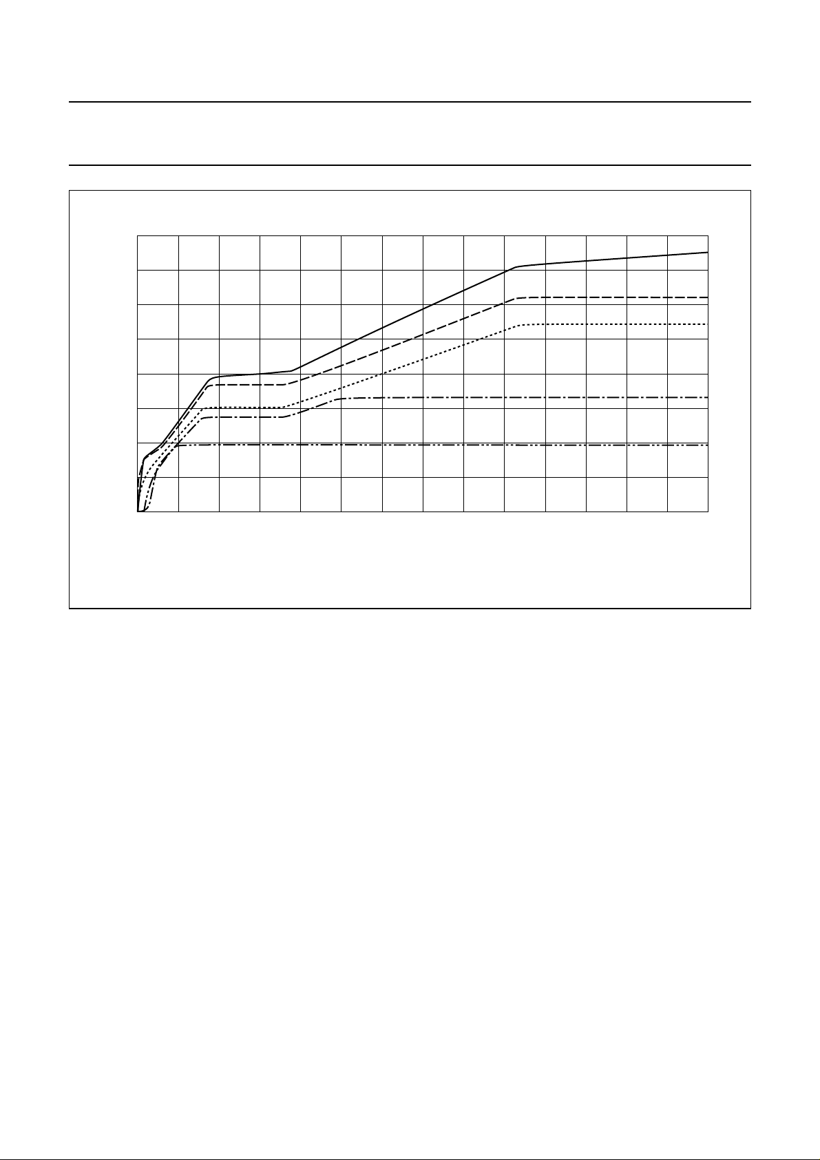
handbook, full pagewidth
8
voltages
(V)
6
4
2
0
0 0.01
0.02 0.05
0.040.03
TEA1097
FCA049
LN
SLPE
V
BB
V
DD
MICS
(A)
0.070.06
I
line
Fig.5 Main DC voltages as a function of line current.
EXTERNAL SUPPLY (PINS ESI AND VBB)
The TEA1097 can be supplied by the line as well as by
external power sources (voltage or current sources) that
must be connected to pin ESI.
The IC will choose which supply to use according to the
voltage it can provide. A voltage supply on ESI is efficient
only if its value is greater than the working voltage of the
internal V
voltage stabilizer. Otherwise the IC continues
BB
to be line powered. The current consumed on this source
is at least equal to the internal consumption. It depends on
the voltage difference between the value forced on ESI
and the working voltage of the internal stabilizer.
The current required increases with the voltage difference
to manage. The excess current compared to the internal
consumption becomes then available for other purposes
such as supplying a loudspeaker amplifier. The voltage
source should not exceed 6 V. If the value of the external
voltage source can be lower than the working voltage of
the internal stabilizer, an external diode is required to avoid
reverse current flowing into the external power supply.
SUPPLY FOR MICROCONTROLLERS (PIN V
V
DD
The voltage on V
supply point follows the voltage on V
DD
DD
)
BB
with a difference equal to 250 mV (typ.) and is internally
limited to 3.35 V. This voltage is temperature
compensated. This supply point can provide a current up
to 3 mA (typ.). Its internal consumption stays low (a few
10 nA) as long as VDD does not exceed 1.5 V (see Fig.6).
An external voltage can be connected on VDD with limited
extra consumption on VDD (typically 100 µA). This voltage
source should not be lower than 3.5 V and higher than 6 V.
VBB and VDD can supply external circuits in the limits of
currents provided either from the line or from pin ESI,
taking into account the internal current consumption.
In case of current source, the voltage on VBB and ESI
depends on the current available. It is internally limited to
6.6 V. The current source should not exceed 140 mA.
1999 Apr 08 9
Philips Semiconductors Product specification
Speech and loudspeaker amplifier IC with
auxiliary inputs/outputs and analog multiplexer
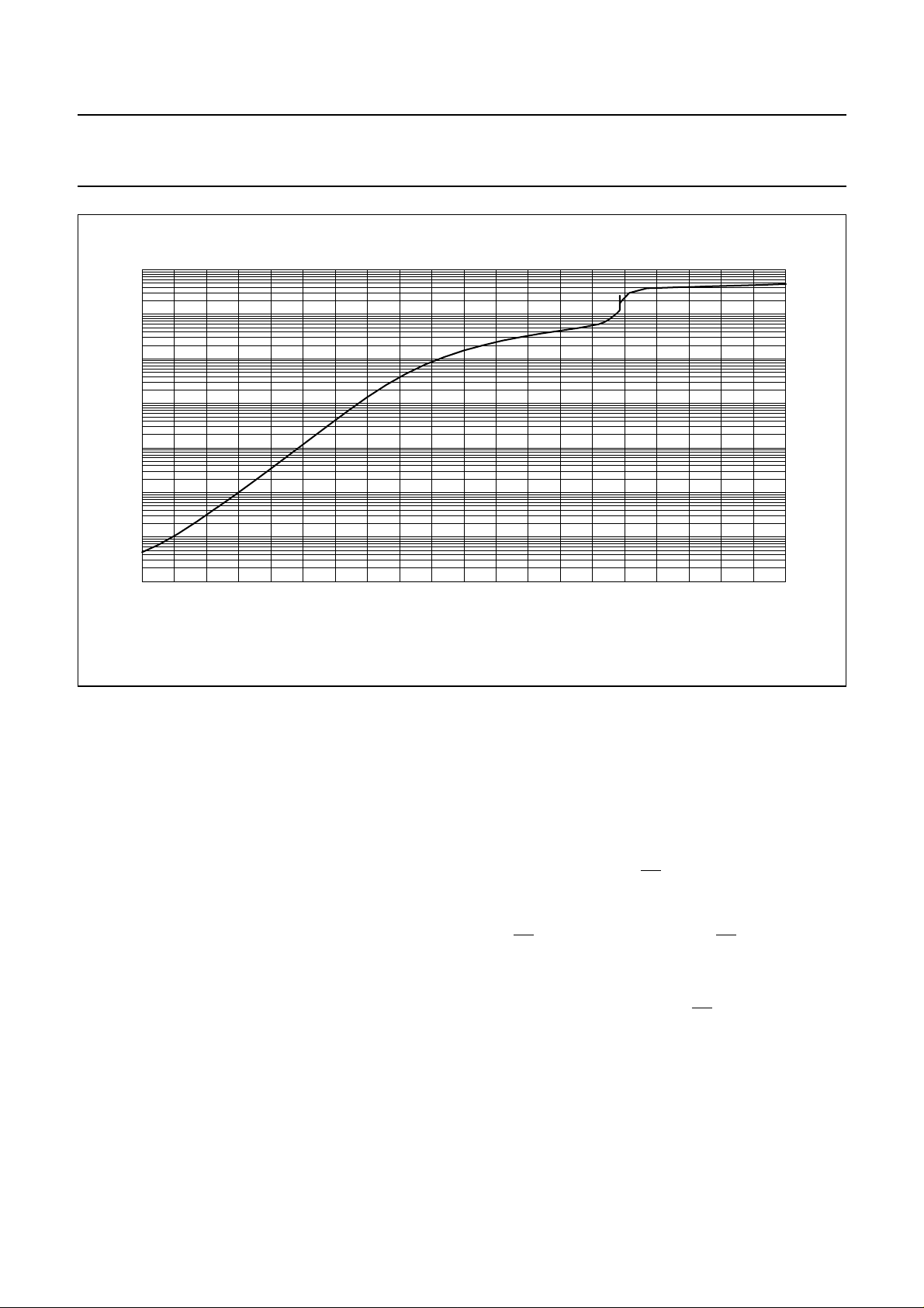
8
10
handbook, full pagewidth
I
DD
(pA)
7
10
6
10
5
10
4
10
3
10
2
10
10
1.0
1.5 2.5 3.0
2.0
TEA1097
FCA050
VDD (V)
Fig.6 Current consumption on VDD.
SUPPLY FOR MICROPHONE (PINS MICS AND GNDTX)
The MICS output can be used as a supply for an electret
microphone. Its voltage is equal to 2 V; it can source
current up to 1 mA and has an output impedance equal to
200 Ω.
L
OW VOLTAGE BEHAVIOUR
For line currents below 9 mA, the reference voltage is
automatically adjusted to a lower value; the VBB voltage
follows the SLPE voltage with 250 mV difference.
The excess current available for other purposes than DC
biasing of the IC becomes small. In this low voltage area,
the IC has limited performances.
When the VBB voltage reaches 2.7 V, the VBB detector of
the receive dynamic limiter on pin LSAO acts continuously,
discharging the capacitor at pin DLC. In the DC condition,
the loudspeaker is automatically disabled below this
voltage.
When V
becomes lower than 2.5 V, the TEA1097 is
BB
forced in a low voltage mode whatever the levels on the
logic inputs are. It is a speech mode with reduced
performances only enabling the microphone channel
(between the MIC inputs and LN) and the earpiece
amplifier. These two channels are able to deliver signals
for line currents as small as 3 mA. The HFC input is tied to
GND sinking a current equal to 300 µA (typ.).
P
OWER-DOWN MODE (PINS PD AND AUXC)
To reduce current consumption during dialling or register
recall (flash), the TEA1097 is provided with a power-down
PD). When the voltage on pins PD and AUXC is
input (
LOW, the current consumption from VBB and VDD is
reduced to 460 µA (typ.). Therefore a capacitor of 470 µF
connected to pin VBB is sufficient to power the TEA1097
during pulse dialling or flash. The PD input has a pull-up
structure, while AUXC has a pull-down structure. In this
mode, the capacitor C
is internally disconnected.
REG
1999 Apr 08 10

Philips Semiconductors Product specification
Speech and loudspeaker amplifier IC with
auxiliary inputs/outputs and analog multiplexer
RINGER MODE (PINS ESI, VBB, AUXC AND PD)
The TEA1097 is designed to be activated during the
ringing phase. The loudspeaker amplifier can be used for
the melody signal. The IC must be powered by an external
supply on pin ESI, while applying a HIGH level on the logic
input AUXC and a LOW level on the
HFRX input and the LSAO output are activated, in order to
limit the current consumption. Some dynamic limiting is
provided to prevent VBB from being discharged below
2.7 V.
Transmit channels (pins MIC+, MIC−, DTMF, TXAUX
and LN)
H
ANDSET MICROPHONE AMPLIFIER (PINS MIC+, MIC− AND
LN)
The TEA1097 has symmetrical microphone inputs.
The input impedance between MIC+ and MIC− is 70 kΩ
(typ.). The voltage gain between pins MIC+, MIC− and LN
is set to 44.3 dB. Without limitation from the output, the
microphone input stage can accommodate signals up to
18 mV (RMS) at room temperature for 2% of THD.
The microphone inputs are biased at one diode voltage.
Automatic gain control is provided for line loss
compensation.
DTMF
AMPLIFIER (PINS DTMF, LN AND RECO)
The TEA1097 has an asymmetrical DTMF input. The input
impedance between pin DTMF and GND is 20 kΩ (typ.).
The voltage gain between pins DTMF and LN is set to
25.35 dB. Without limitation from the output, the input
stage can accommodate signals up to 180 mV (RMS) at
room temperature for 2% of THD.
When the DTMF amplifier is enabled, dialling tones may
be sent on the line. These tones can be heard in the
earpiece or in the loudspeaker at a low level. This is called
the confidence tone. The voltage attenuation between pins
DTMF and RECO is typically equal to −16.5 dB.
The DC biasing of this input is 0 V.
The automatic gain control has no effect on these
channels.
PD input. Only the
A
UXILIARY TRANSMIT AMPLIFIER (PINS TXAUX AND LN)
The TEA1097 has an asymmetrical auxiliary input TXAUX.
The input impedance between pins TXAUX and GND is
20 kΩ (typ.). The voltage gain between pins TXAUX and
LN is set to 12.5 dB. Without limitation from the output, the
input stage can accommodate signals up to 1.2 V (RMS)
at room temperature for 2% of THD. The TXAUX input is
biased at two diodes voltage.
Automatic gain control is provided for line loss
compensation.
M
ICROPHONE MONITORING ON TXOUT (PINS MIC+, MIC−
AND TXOUT)
The voltage gain between the microphone inputs MIC+,
MIC− and the output TXOUT is set to 49.8 dB. This
channel gives an image of the signal sent on the line while
speaking in the handset microphone. Using external
circuitry, this signal can be used for several purposes such
as sending dynamic limiting or anti-howling in a listening-in
application. The TXOUT output is biased at two diodes
voltage.
The automatic gain control has no effect on these
channels.
Receive channels (pins IR, RAUX, RECO, GARX and
QR)
RX
AMPLIFIER (PINS IR AND RECO)
The receive amplifier has one input IR which is referred to
the line. The input impedance between pins IR and LN is
20 kΩ (typ.) and the DC biasing between these pins is
equal to one diode voltage. The gain between pins IR
(referenced to LN) and RECO is typically equal to 29.7 dB.
Without limitation from the output, the input stage can
accommodate signals up to 50 mV (RMS) at room
temperature for 2% of THD.
This receive amplifier has a rail-to-rail output RECO, which
is designed for use with high-ohmic (real) loads (larger
than 5 kΩ). This output is biased at two diodes voltage.
Automatic gain control is provided for line loss
compensation.
TEA1097
1999 Apr 08 11
 Loading...