


INTEGRATED CIRCUITS
DATA SH EET
TEA1096; TEA1096A
Speech and listening-in IC
Product Specification
File under Integrated Circuits, IC03
Philips Semiconductors
November 1994

Philips Semiconductors Product Specification
Speech and listening-in IC TEA1096; TEA1096A
FEATURES
• Line Interface with:
– active set impedance (adjustable)
– voltage regulator with adjustable DC voltage
– low voltage circuit for parallel operation
• Interface to peripheral circuits with:
– supply VDD for microcontroller
– stabilized supply voltage (VBB) which is:
available for peripheral circuits
adjustable (TEA1096 only)
– Dual-Tone MultiFrequency (DTMF) signal input
– power-down function for pulse dialling/flash
– mute function to disable speech during dialling
• Microphone amplifier with:
– symmetrical high impedance inputs
– externally adjustable gain
– AGC; line-loss compensation
– dynamic limiter
– microphone mute function
• Receiving amplifier with:
– externally adjustable gain
– confidence tone during dialling
– double anti-sidetone circuit for long and short lines
– AGC; line-loss compensation
– earpiece protection by soft clipping.
• Listening-in circuit with:
– loudspeaker amplifier
– dynamic limiter to prevent distortion at any supply
condition
– volume control via a potentiometer
– fixed gain of 35.5 dB
– disable function
– gain control input (TEA1096A only).
APPLICATIONS
• Line-powered telephone sets with listening-in/line
monitoring function.
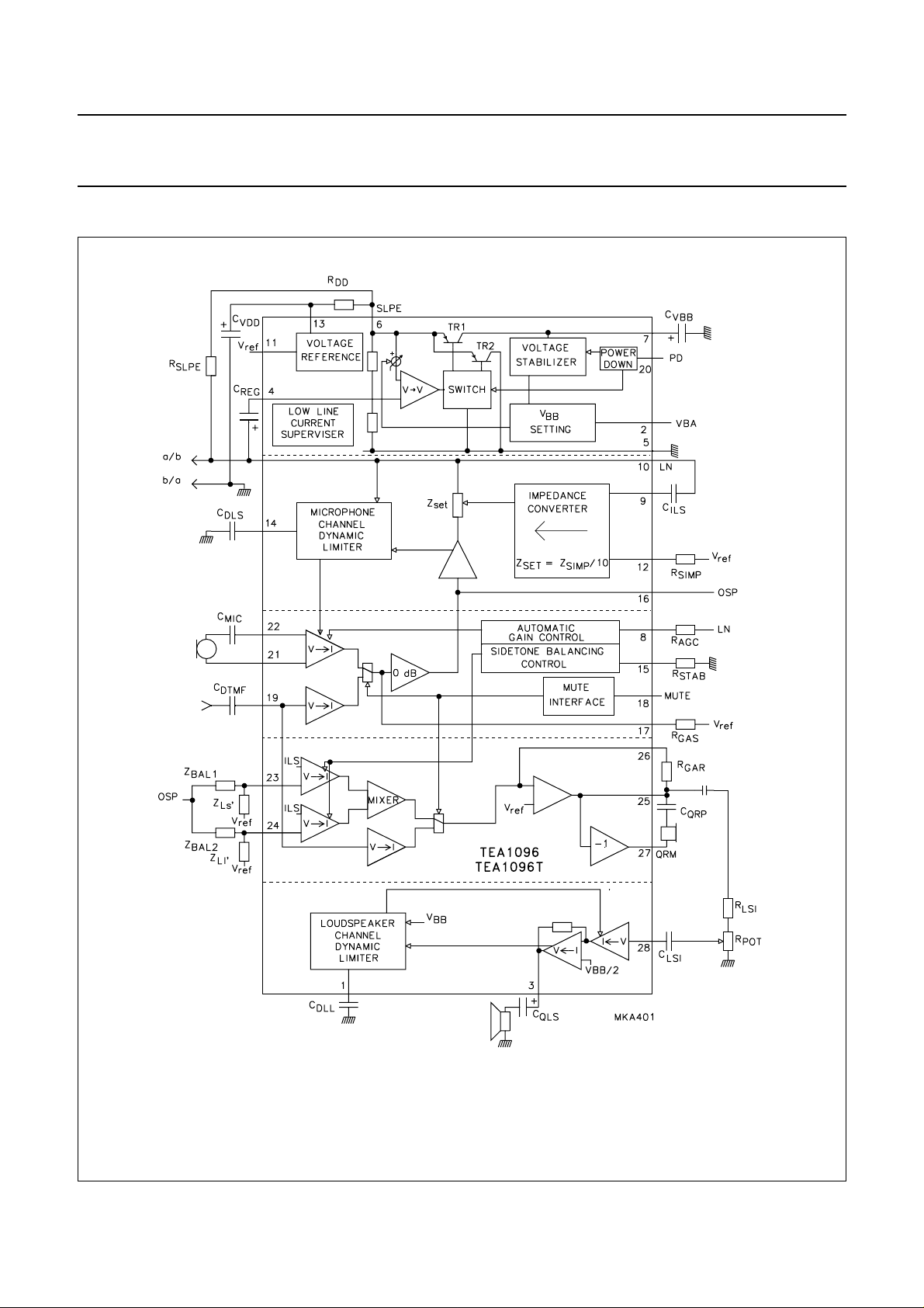
DIFFERENCES BETWEEN TEA1096 AND TEA1096A
The TEA1096 offers via input VBA an adjustable stabilized
supply voltage V
stabilized voltage VBB.
The TEA1096A offers a DC gain control input VCI to set
the loudspeaker volume, whereas the TEA1096 offers
volume control via a potentiometer.
GENERAL DESCRIPTION
The TEA1096 and TEA1096A are bipolar ICs intended for
use in line powered telephone sets. They offer a
speech/transmission function, listening-in and line
monitoring facilities of the received line signal via the
loudspeaker.
The devices incorporate a line interface block, a
microphone and DTMF amplifier, a receiving amplifier, a
supply function, a loudspeaker amplifier, and a dynamic
limiter in the transmission channel and the listening-in
channel.
, whereas the TEA1096A offers a fixed
BB
ORDERING INFORMATION
TYPE NUMBER
NAME DESCRIPTION VERSION
TEA1096 DIP28 plastic dual in-line package; 28 leads (600 mil) SOT117-1
TEA1096A DIP28 plastic dual in-line package; 28 leads (600 mil) SOT117-1
TEA1096T SO28 plastic small outline package; 28 leads; body width 7.5 mm SOT136-1
TEA1096AT SO28 plastic small outline package; 28 leads; body width 7.5 mm SOT136-1
November 1994 2
PACKAGE
Philips Semiconductors Product Specification
Speech and listening-in IC TEA1096; TEA1096A
QUICK REFERENCE DATA
SYMBOL PARAMETER CONDITIONS MIN. TYP. MAX. UNIT
I
line
I
DD
I
DD(PD)
I
BB(PD)
V
SLPE
V
DD
V
BB
G
vtx
∆G
vtxr
G
vrx
∆G
vrxr
∆G
trx
G
vlx
V
LN(p-p)
V
QLS(p-p)
T
amb
line current normal condition 15 − 140 mA
with reduced performance −−15 mA
current consumption from pin V
PD = LOW − 2.4 2.9 mA
DD
during normal operation
current consumption from
capacitor C
VDD
during
PD = HIGH − 100 150 µA
power-down
current consumption from
capacitor C
VBB
during
PD = HIGH − 350 500 µA
power-down
stabilized voltage (line interface) 4.2 4.45 4.7 V
supply voltage for microcontroller RDD= 390 Ω;
− 3.5 − V
IP=0mA
R
= 390 Ω;
DD
− 3.1 − V
IP=1mA
stabilized supply voltage 3.4 3.6 3.8 V
voltage gain from pin MICP or
MICM to LN
voltage gain adjustment with
R
GAS
voltage gain from pin LN to QRP
or QRM
voltage gain adjustment with
R
GAR
line-loss compensation R
voltage gain from pin LSI to QLS V
maximum output voltage swing
V
= 2 mV (RMS);
MIC
R
= 90.9 kΩ;
GAS
I
=20mA
line
51 52 53 dB
−19 − 0dB
V
= 50 mV (RMS);
line
R
= 90.9 kΩ;
GAR
I
= 20 mA
line
−3.5 −2.5 −1.5 dB
−12 − 8dB
= 100 kΩ 567dB
AGC
= 10 mV (RMS) 34 35.5 37 dB
LSI
− 3.65 4.3 V
on pin LN (peak-to-peak value)
output voltage between pins QLS
V
LSI
=18mV; I
= 20 mA 2.5 2.9 − mA
line
and VEE (peak-to-peak value)
operating ambient temperature −25 − +75 °C
November 1994 3
Philips Semiconductors Product Specification
Speech and listening-in IC TEA1096; TEA1096A
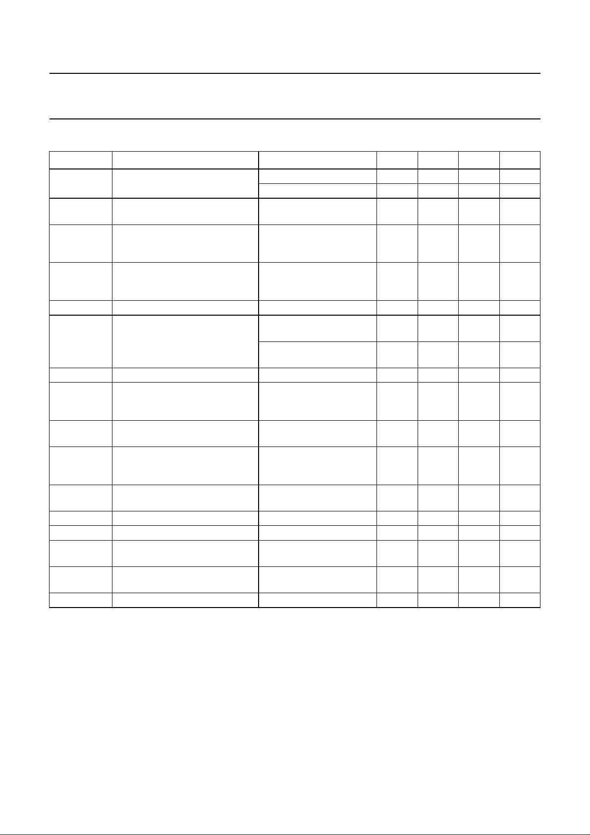
BLOCK DIAGRAMS
Fig.1 Block diagram (TEA1096).
November 1994 4
Philips Semiconductors Product Specification
Speech and listening-in IC TEA1096; TEA1096A
Fig.2 Block diagram (TEA1096A).
November 1994 5
Philips Semiconductors Product Specification
Speech and listening-in IC TEA1096; TEA1096A
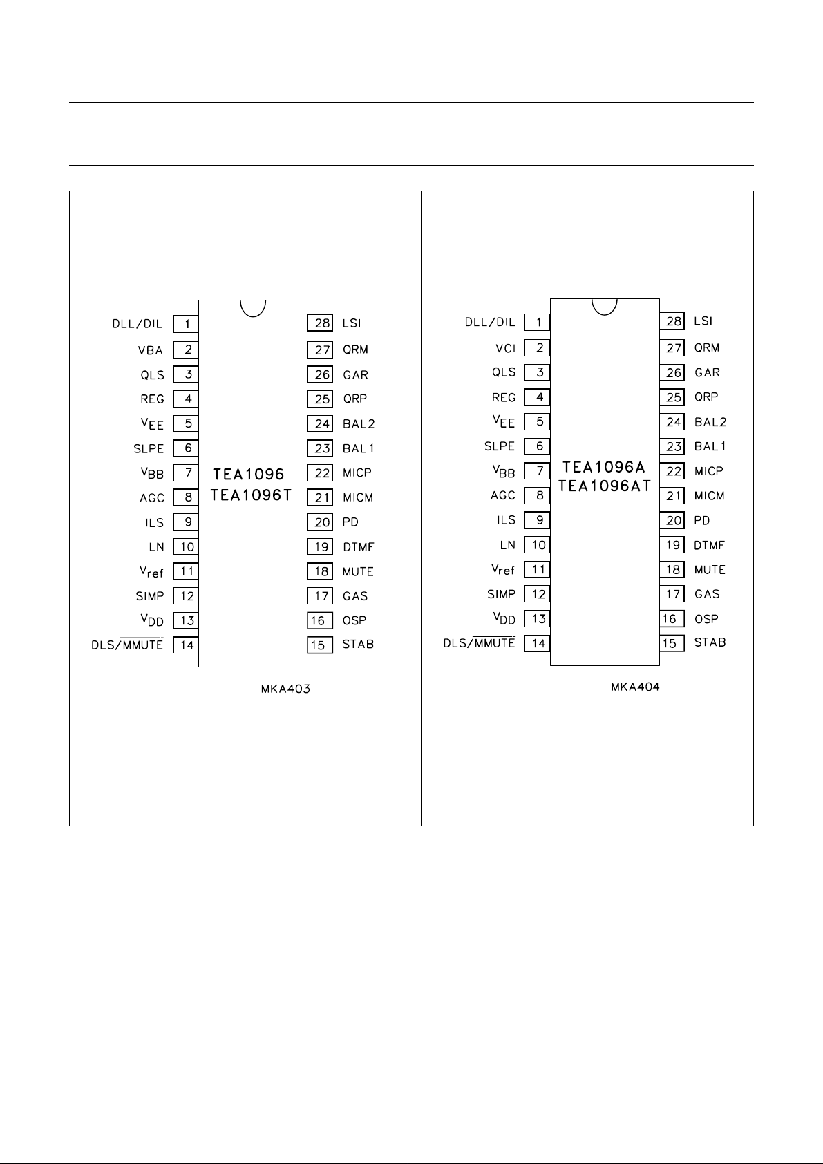
PINNING
SYMBOL
DESCRIPTION
TEA1096 TEA1096A
DLL/DIL 1 1 dynamic limiter and disable input for loudspeaker amplifier
VBA 2 − VBB voltage adjustment
VCI − 2 volume control input for loudspeaker amplifier
QLS 3 3 loudspeaker amplifier output
REG 4 4 decoupling line voltage stabilizer
PINS
V
EE
5 5 negative line terminal (ground reference)
SLPE 6 6 stabilized voltage, connection for slope resistor
V
BB
7 7 stabilized supply voltage for listening-in circuitry
AGC 8 8 automatic gain control
ILS 9 9 input line signal
LN 10 10 positive line terminal
V
ref
11 11 reference voltage output
SIMP 12 12 set impedance input
V
DD
DLS/
MMUTE 14 14 dynamic limiter for sending and microphone mute
13 13 supply voltage for speech circuitry/peripherals
STAB 15 15 reference current adjustment
OSP 16 16 sending preamplifier output
GAS 17 17 sending gain adjustment
MUTE 18 18 mute input to select speech or DTMF dialling
DTMF 19 19 dual-tone multi-frequency (DTMF) input
PD 20 20 power-down input
MICM 21 21 inverting microphone amplifier input
MICP 22 22 non-inverting microphone amplifier input
BAL1 23 23 connection for balance network 1
BAL2 24 24 connection for balance network 2
QRP 25 25 non-inverting receiving amplifier output
GAR 26 26 receiving gain adjustment
QRM 27 27 inverting receiving amplifier output
LSI 28 28 loudspeaker amplifier input
November 1994 6
Philips Semiconductors Product Specification
Speech and listening-in IC TEA1096; TEA1096A
Fig.3 Pin configuration (TEA1096).
November 1994 7
Fig.4 Pin configuration (TEA1096A).
Philips Semiconductors Product Specification
Speech and listening-in IC TEA1096; TEA1096A
FUNCTIONAL DESCRIPTION
Remark: all data given in this chapter are typical values
except when otherwise specified.
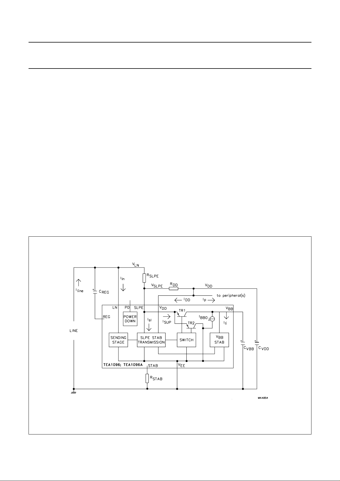
Supply pins SLPE, LN, V
, VBB, VDD, REG and PD
EE
The supply for the TEA1096/TEA1096A and its
peripherals is obtained from the telephone line. The
circuits regulate the line voltage and generate their own
supply voltages V
and VBB to power the transmission
DD
part and the loudspeaker amplifier respectively.
As can be seen from Fig.5, the line current (I
) is split
line
between the sending output stage (Iln), the circuitry
connected to SLPE (Isl), the transmission circuit (IDD), the
peripheral circuits (Ip) and the current switch (I
SUP
). It can
be shown that:
I
SUP=Iline
− (Iln+Isl+IDD+IP)
With nominal conditions where:
Iln= 5 mA, Isl= 0.3 mA and IDD= 2.4 mA
it therefore follows that I
SUP
≈ I
− 7.7 mA − IP.
line
The remaining current I
part. The current consumption I
is available for the listening-in
SUP
of the listening-in
BB0
circuitry is 2.5 mA. To power the loudspeaker, the line
current has to be more than 10 mA.
The voltage at SLPE is stabilized at 4.45 V nominal. The
DC line voltage is regulated at:
VLN=V
SLPE+RSLPE
× (I
line
− Iln).
The supply voltage for the transmission part and
peripheral circuits (VDD) is generated from V
equal to VDD=V
− RDD× (IDD+Ip).
SLPE
SLPE
and is
VBB supplies the listening-in circuitry and is stabilized at
3.6 V nominal.
A resistor connected between pin REG and VEE can be
used to decrease the SLPE voltage while maintaining V
BB
at its nominal value, whereas a resistor connected
between pin REG and pin SLPE will increase the SLPE
voltage while maintaining VBB at its nominal value. When
adjusting the SLPE voltage to a lower value, care should
be taken that the V
is at least 0.4 V higher than V
SLPE
BB
(VBB supply efficiency).
Fig.5 Supply arrangement.
November 1994 8
Philips Semiconductors Product Specification
Speech and listening-in IC TEA1096; TEA1096A
The function of the current switch TR1-TR2 is to reduce
distortion of large line signals. Current I
VBB via TR1, when V
V
is lower, this current is shunted to VEE via TR2. All
SLPE
is higher than VBB+ 0.4 V. When
SLPE
is supplied to
SUP
excess line current, not used for internal supply is
consumed in the VBB stabilizer or directly shunted to VEE.
To reduce the current consumption during pulse dialling,
the TEA1096/TEA1096A are provided with a power-down
(PD) input. The PD input has a pull-down structure. When
the voltage on PD is HIGH, the current consumption from
VDD capacitor C
point 350 µA. The capacitors C
is 100 µA and from the VBB supply
VDD
(100 µF) and C
VDD
VBB
(470 µF) are sufficient to power theTEA1096/TEA1096A
during pulse dialling/flash.
V
voltage adjustment: pin VBA (TEA1096 only)
BB
A resistor connected between pins VBA and V
can be
EE
used to increase the VBB voltage, whereas a resistor
connected between pins VBA and VBB will decrease the
VBB voltage. When adjusting the VBB voltage to a higher
value, care should be taken that V
is at least 0.4 V
SLPE
higher than VBB (VBB supply efficiency).
Sending channel: pins MICP, MICM, DTMF, GAS, OSP, LN, MUTE, DLS and AGC
The TEA1096/TEA1096A has symmetrical microphone
inputs MICP, MICM with an input resistance of 64 kΩ
between MICP and MICM (2 × 32 kΩ). In the speech mode
(MUTE = LOW), the overall gain from MICP-MICM to LN
can be adjusted from 33 dB to 52 dB to suit specific
requirements. The gain is proportional to the value of R
and equals 52 dB with R
capacitor C
connected in parallel with R
GAS
= 90.9 kΩ and I
GAS
= 20 mA. A
line
GAS
GAS
can be
used to provide a first-order low-pass filter.
Automatic gain control (AGC) is provided for line-loss
compensation as well as dynamic limitation for reduction
of the distortion of the transmitted signal on the line. The
microphone amplifier can be disabled by short-circuiting
pin DLS to VEE (secret function) and can be muted into
DTMF mode by applying a HIGH level on pin MUTE.
The TEA1096/TEA1096A has an asymmetrical DTMF
input with an input resistance of 20 kΩ. In the DTMF mode,
the overall gain from DTMF to LN is proportional to R
GAS
and is 26.5 dB less than the microphone amplifier gain.
Switch-over from one mode to the other is click-free.
,
Fig.6 Sending channel.
November 1994 9
Philips Semiconductors Product Specification
Speech and listening-in IC TEA1096; TEA1096A
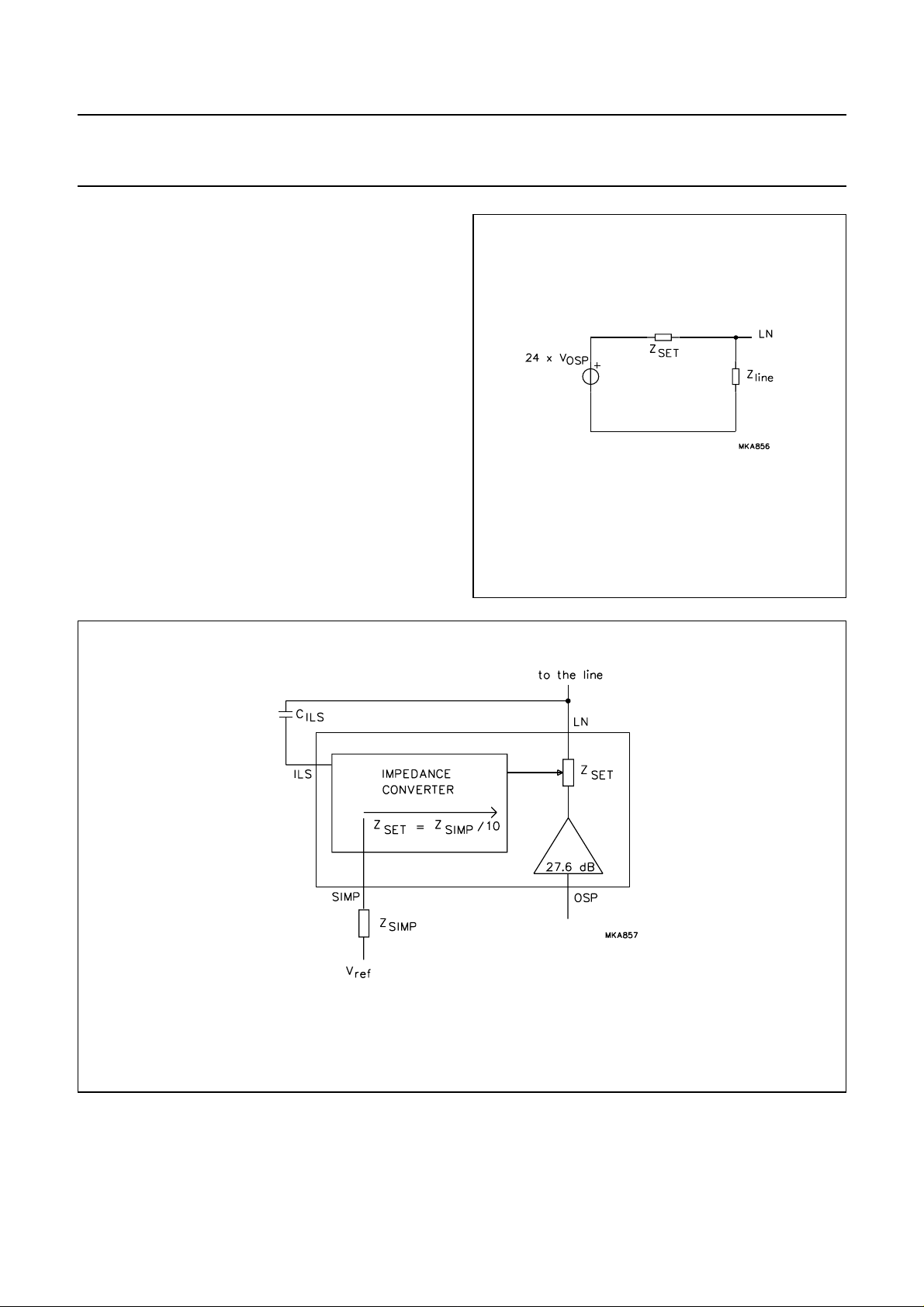
It can be calculated from Fig.7 that the AC modulator gain
can be written:
V
LN
• providing
-------------V
OSP
Z
SET=Zline
-----------------------------------------------------( Z
Z
line
Z
line
SET
) 24×+
12==
• Gv (LN to OSP) = 21.6 dB.
The frequency response for audio frequencies of the
sending channel is flat in this case for a complex line
termination.
Set impedance: pins ILS, SIMP and LN
The TEA1096/TEA1096A provides an active set
impedance in both the receiving and sending conditions,
thus allowing a flat frequency response for a complex line
impedance, without the need for any extra compensation
network.
As can be derived from Fig.8 the set impedance Z
10 times lower than Z
SIMP
.
SET
is
Fig.7 AC modulator equivalent model.
Fig.8 Set impedance.
November 1994 10
 Loading...