

Philips TEA1095T-C1, TEA1095-C1, TEA1095TS-C1 Datasheet

DATA SH EET
Product specification
Supersedes data of 1996 Mar 22
File under Integrated Circuits, IC03
1997 Nov 25
INTEGRATED CIRCUITS
TEA1095
Voice switched speakerphone IC
1997 Nov 25 2
Philips Semiconductors Product specification
Voice switched speakerphone IC TEA1095
FEATURES
• External power supply with power-down function
• Transmit channel with:
– externally adjustable gain
– transmit mute function
• Receive channel with:
– externally adjustable gain
– logarithmic volume control via a linear potentiometer
– receive mute function
• Duplex controller consisting of:
– signal envelope and noise envelope monitors for both
channels with:
externally adjustable sensitivity
externally adjustable signal envelope time constant
externally adjustable noise envelope time constant
– decision logic with:
externally adjustable switch-over timing
externally adjustable idle mode timing
externally adjustable dial tone detector in receive
channel
– voice switch control with:
adjustable switching range
constant sum of gain during switching
constant sum of gain at different volume settings.
APPLICATIONS
• Mains, battery or line-powered telephone sets
• Cordless telephones
• Answering machines
• Fax machines
• Hands-free car kits.
GENERAL DESCRIPTION
The TEA1095 is a bipolar circuit, that in conjunction with a
member of the TEA106X, TEA111X families of
transmission or TEA1096 transmission/listening-in circuits
offers a hands-free function. It incorporates a transmit
amplifier, a receiver channel amplifier and a duplex
controller with signal and noise monitors on both channels.
ORDERING INFORMATION
TYPE
NUMBER
PACKAGE
NAME DESCRIPTION VERSION
TEA1095 DIP24 plastic dual in-line package; 24 leads (600 mil) SOT101-1
TEA1095T SO24 plastic small outline package; 24 leads; body width 7.5 mm SOT137-1
TEA1095TS SSOP24 plastic shrink small outline package; 24 leads; body width 5.3 mm SOT340-1
1997 Nov 25 3
Philips Semiconductors Product specification
Voice switched speakerphone IC TEA1095
QUICK REFERENCE DATA
VBB=5V; V
GND
= 0 V; f = 1 kHz; T
amb
=25°C; MUTETX = LOW ; MUTERX = LOW; PD = LOW; R
VOL
=0Ω; measured
in test circuit of Fig.11; unless otherwise specified.
SYMBOL PARAMETER CONDITIONS MIN. TYP. MAX. UNIT
V
BB
supply voltage 2.9 − 12.0 V
I
BB
current consumption from pin V
BB
− 2.7 3.8 mA
G
vtx
voltage gain from TXIN to TXOUT in
transmit mode
V
TXIN
= 1 mV (RMS);
R
GATX
= 30.1 kΩ
− 15.5 − dB
∆G
vtxr
voltage gain adjustment with R
GATX
−15.5 − +24.5 dB
G
vrx
voltage gain from RXIN to RXOUT in
receive mode
V
RXIN
= 20 mV (RMS);
R
GARX
= 16.5 kΩ
− 6.5 − dB
∆G
vrxr
voltage gain adjustment with R
GARX
−20.5 − +19.5 dB
SWRA switching range − 40 − dB
∆SWRA switching range adjustment with R
SWR
referenced to
R
SWR
= 365 kΩ
−40 − +12 dB
T
amb
operating ambient temperature −25 − +75 °C
1997 Nov 25 4
Philips Semiconductors Product specification
Voice switched speakerphone IC TEA1095
BLOCK DIAGRAM
Fig.1 Block diagram.
handbook, full pagewidth
BUFFER
BUFFER
BUFFER
BUFFER
LOG
LOG
LOGIC
VOICE
SWITCH
VOLUME
CONTROL
V
BB
C
TXIN
R
MIC
R
TSEN
V
ref
R
GATX
R
IDT
C
SWT
R
STAB
R
SWR
R
VOL
C
TSEN
C
TENV
C
TNOI
C
RNOI
C
RENV
C
RSEN
R
RSEN
V
dt
R
GARX
V
BB
PD
7
13
15 MUTETX
TRANSMIT CHANNEL
to transmission
circuit
DUPLEX CONTROLLER
TEA1095
18
24
23
22
19
20
21
4
5
1
TXIN
TSEN
TENV
TNOI
RNOI
RENV
RSEN
GARX
2
RXOUT
RXIN
VOL 8
2
9
10
11
12
14
16
17
6
SWR
STAB
SWT
IDT
TXGND
TXOUT
GATX
GND
to loudspeaker
amplifier
MUTERX
RECEIVE CHANNEL
13
mV
13 mV
ATTENUATOR
from transmission
circuit
V I
I V
V I
I V
MBG350
1997 Nov 25 5
Philips Semiconductors Product specification
Voice switched speakerphone IC TEA1095
PINNING
SYMBOL PIN DESCRIPTION
MUTERX 1 receiver channel mute input
RXIN 2 receiver amplifier input
n.c. 3 not connected
GARX 4 receiver gain adjustment
RXOUT 5 receiver amplifier output
GND 6 ground reference
V
BB
7 supply voltage input
VOL 8 receiver volume adjustment
SWR 9 switching range adjustment
STAB 10 reference current adjustment
SWT 11 switch-over timing adjustment
IDT 12 idle mode timing adjustment
PD 13 power-down input
TXGND 14 ground reference for the transmit
channel
MUTETX 15 transmit channel mute input
TXOUT 16 transmit amplifier output
GATX 17 transmit gain adjustment
TXIN 18 transmit amplifier input
RNOI 19 receive noise envelope timing
adjustment
RENV 20 receive signal envelope timing
adjustment
RSEN 21 receive signal envelope sensitivity
adjustment
TNOI 22 transmit noise envelope timing
adjustment
TENV 23 transmit signal envelope timing
adjustment
TSEN 24 transmit signal envelope sensitivity
adjustment
Fig.2 Pin configuration.
handbook, halfpage
TEA1095
MBG349
1
2
3
4
5
6
7
8
9
10
11
12
MUTERX
RXIN
n.c.
GARX
RXOUT
GND
V
BB
VOL
SWR
STAB
SWT
IDT
TSEN
TENV
TNOI
RSEN
RENV
RNOI
TXIN
GATX
TXOUT
MUTETX
TXGND
PD
24
23
22
21
20
19
18
17
16
15
14
13
1997 Nov 25 6
Philips Semiconductors Product specification
Voice switched speakerphone IC TEA1095
FUNCTIONAL DESCRIPTION
The values given in the functional description are typical
values except when otherwise specified.
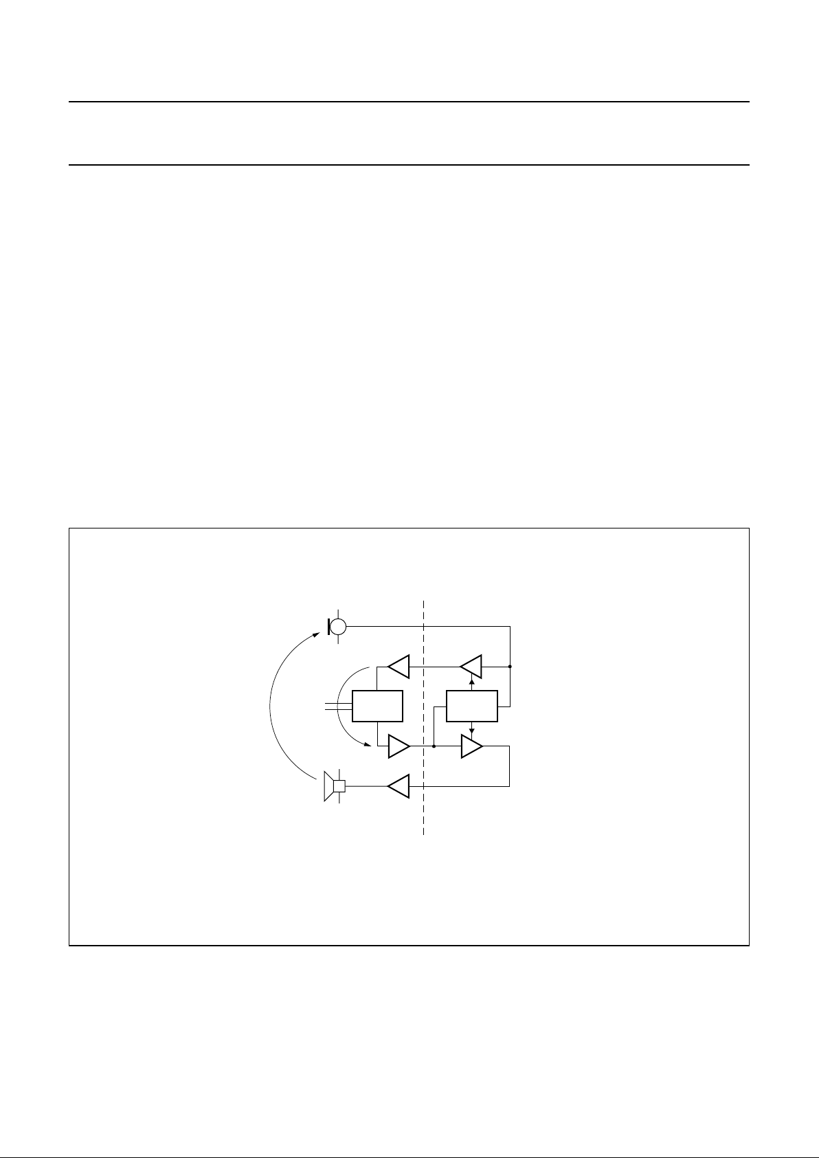
A principle diagram of the TEA1096 is shown on the left
side of Fig.3. The TEA1096 is a transmission and
listening-in circuit. It incorporates a receiving amplifier for
the earpiece, a transmit amplifier for the microphone, a
loudspeaker amplifier and a hybrid. For more details on the
TEA1096 circuit (please refer to
Data Handbook IC03
).
The right side of Fig.3 shows a principle diagram of the
TEA1095, a hands-free add-on circuit with a transmit
amplifier, a receiver amplifier and a duplex controller.
As can be seen from Fig.3, a loop is formed via the
sidetone network in the transmission circuit and the
acoustic coupling between loudspeaker and microphone
of the hands-free circuit. When this loop gain is greater
than 1, howling is introduced. In a full duplex application,
this would be the case. The loop-gain has to be much
lower than 1 and therefore has to be decreased to avoid
howling. This is achieved by the duplex controller. The
duplex controller of the TEA1095 detects which channel
has the ‘largest’ signal and then controls the gains of the
transmit amplifier and the receiver amplifier such that the
sum of the gains remains constant. As a result, the circuit
can be in three stable modes:
1. Transmit mode (Tx mode): the gain of the transmit
amplifier is at its maximum and the gain of the receiver
amplifier is at its minimum.
2. Receive mode (Rx mode): the gain of the receiver
amplifier is at its maximum and the gain of the transmit
amplifier is at its minimum.
3. Idle mode: the gain of the amplifiers is halfway
between their maximum and minimum value.
The difference between the maximum gain and minimum
gain is called the switching range.
Fig.3 Hands-free telephone set principles.
handbook, full pagewidth
MBG358
HYBRID
DUPLEX
CONTROL
telephone
line
acoustic
coupling
sidetone
TEA1096 TEA1095
1997 Nov 25 7
Philips Semiconductors Product specification
Voice switched speakerphone IC TEA1095
Supply: pins VBB, GND and PD
The TEA1095 must be supplied with an external stabilized
voltage source between pins V
BB
and GND. In idle mode,
without any signal, the internal supply current is 2.7 mA at
VBB=5V.
To reduce current consumption during pulse dialling or
register recall (flash), the TEA1095 is provided with a
power-down (PD) input. When the voltage on PD is HIGH,
the current consumption from VBB is 140 µA.
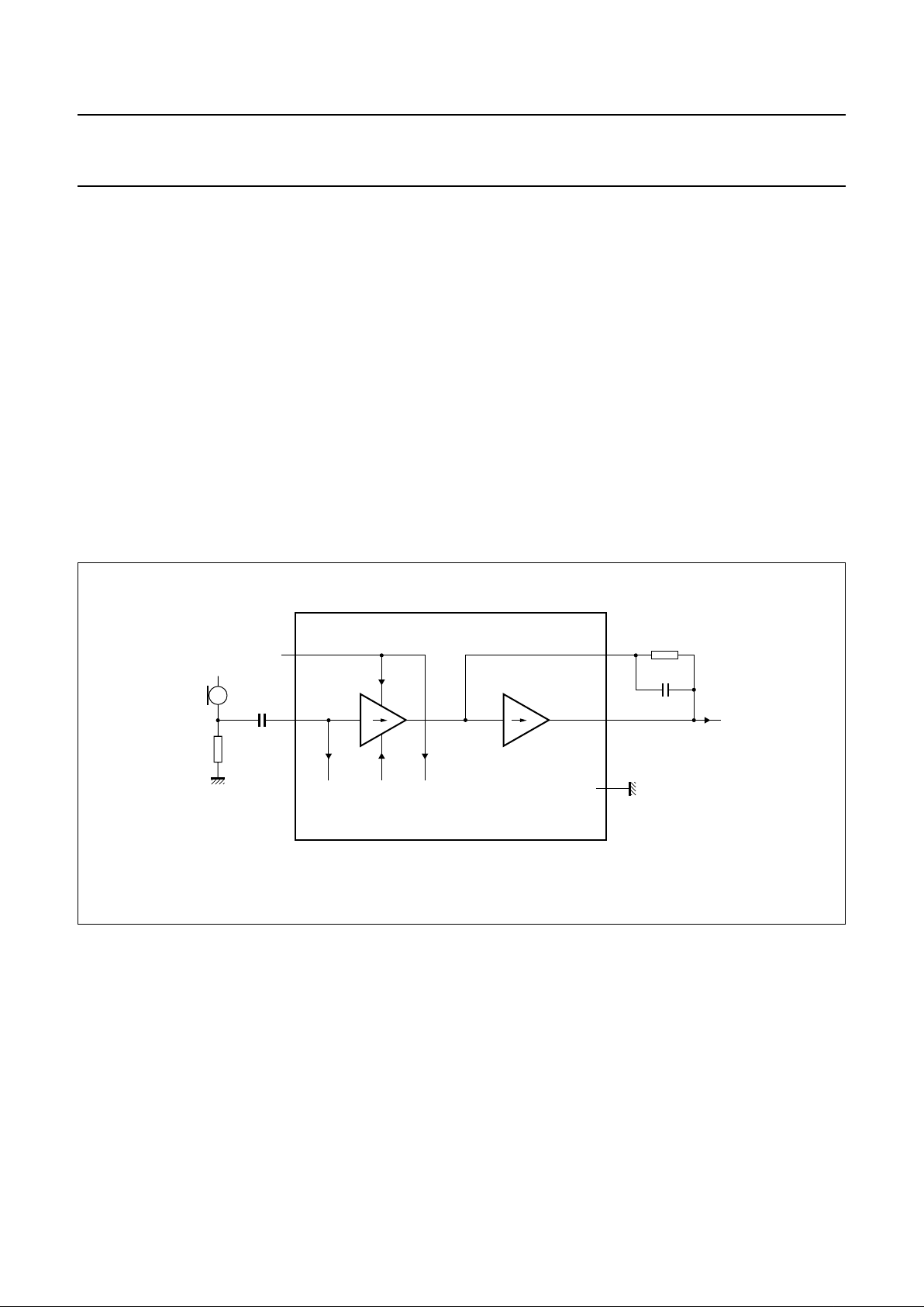
Transmit channel: pins TXIN, GATX, TXOUT, TXGND
and MUTETX
The TEA1095 has an asymmetrical transmit input (TXIN)
with an input resistance of 20 kΩ. The gain of the input
stage varies according to the mode of the TEA1095. In the
transmit mode, the gain is at its maximum; in the receive
mode, it is at its minimum and in the idle mode, it is halfway
between maximum and minimum. Switch-over from one
mode to the other is smooth and click-free. The output
capability at pin TXOUT is 20 µA (RMS).
In the transmit mode, the overall gain of the transmit
amplifier (from pin TXIN to TXOUT) can be adjusted from
0 dB to 40 dB to suit application specific requirements.
The gain is proportional to the value of R
GATX
and equals
15.5 dB with R
GATX
= 30.1 kΩ.
A capacitor must be connected in parallel with R
GATX
to
ensure stability of the transmit amplifier. Together with
R
GATX
, it also provides a first-order low-pass filter.
By applying a HIGH level on pin MUTETX, the transmit
amplifier is muted and the TEA1095 is automatically
forced into the receive mode.
Fig.4 Transmit channel.
handbook, full pagewidth
MBG357
V I I V
C
TXIN
V
BB
R
MIC
MUTETX
TXIN
from
voice
switch
to
envelope
detector
TXGND
TXOUT
GATX
to transmission
circuit
R
GATX
C
GATX
to
logic
1997 Nov 25 8
Philips Semiconductors Product specification
Voice switched speakerphone IC TEA1095
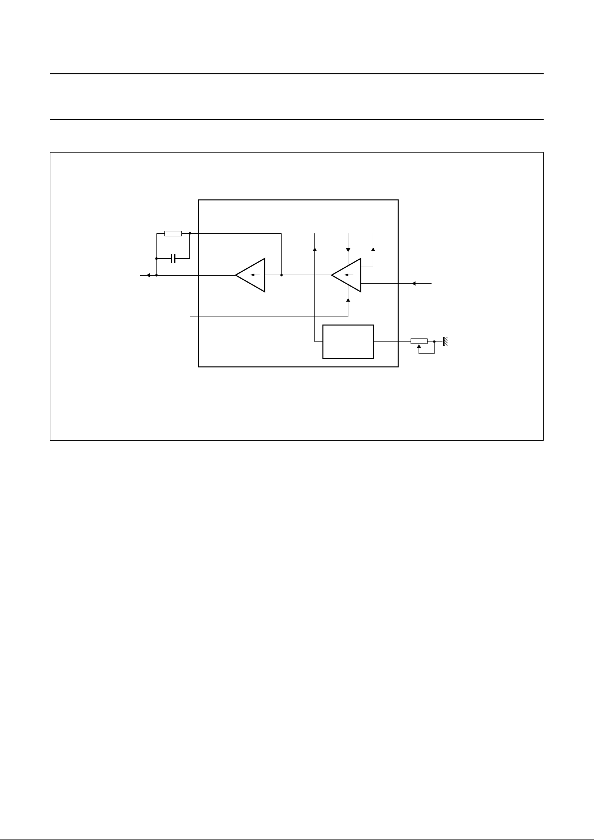
Receive channel
Fig.5 Receive channel.
handbook, full pagewidth
MBG356
V I
I V
R
GARX
C
GARX
GARX
RXOUT
MUTERX
to loudspeaker
amplifier
to/from
voice switch
to
envelope
detector
RXIN
from transmission
circuit
VOL
VOLUME
CONTROL
R
VOL
RECEIVER AMPLIFIER: PINS RXIN, GARX, RXOUT AND
MUTERX
The TEA1095 has an asymmetrical input (RXIN) for the
receiver amplifier with an input resistance of 20 kΩ. The
gain of the input stage varies according to the mode of the
TEA1095. In the receive mode, the gain is at its maximum;
in the transmit mode, it is at its minimum and in the idle
mode, it is halfway between maximum and minimum.
Switch-over from one mode to the other is smooth and
click-free.
In the receive mode, the overall gain of the receive
amplifier can be adjusted from −14 dB to +26 dB to suit
application specific requirements. The gain from RXIN to
RXOUT is proportional to the value of R
GARX
and equals
6.5 dB with R
GARX
= 16.5 kΩ. A capacitor connected in
parallel with R
GARX
can be used to provide a first-order
low-pass filter.
By applying a HIGH level on pin MUTERX, the receiver
amplifier is muted and the TEA1095 is automatically
forced into the transmit mode.
V
OLUME CONTROL: PIN VOL
The receiver amplifier gain can be adjusted with the
potentiometer R
VOL
. A linear potentiometer can be used to
obtain logarithmic control of the gain of the receiver
amplifier. Each 950 Ω increase of R
VOL
results in a gain
loss of 3 dB. The maximum gain reduction with the volume
control is internally limited to the switching range.
Duplex controller
S
IGNAL AND NOISE ENVELOPE DETECTORS: PINS TSEN,
TENV, TNOI, RSEN, RENV
AND RNOI
The signal envelopes are used to monitor the signal level
strength in both channels. The noise envelopes are used
to monitor background noise in both channels. The signal
and noise envelopes provide inputs for the decision logic.
The signal and noise envelopes detectors are shown in
Fig.6.
For the transmit channel, the input signal at TXIN is 40 dB
amplified to TSEN. For the receive channel, the input
signal at RXIN is 0 dB amplified to RSEN. The signals from
TSEN and RSEN are logarithmically compressed and
buffered to TENV and RENV respectively. The sensitivity
of the envelope detectors is set with R
TSEN
and R
RSEN
.
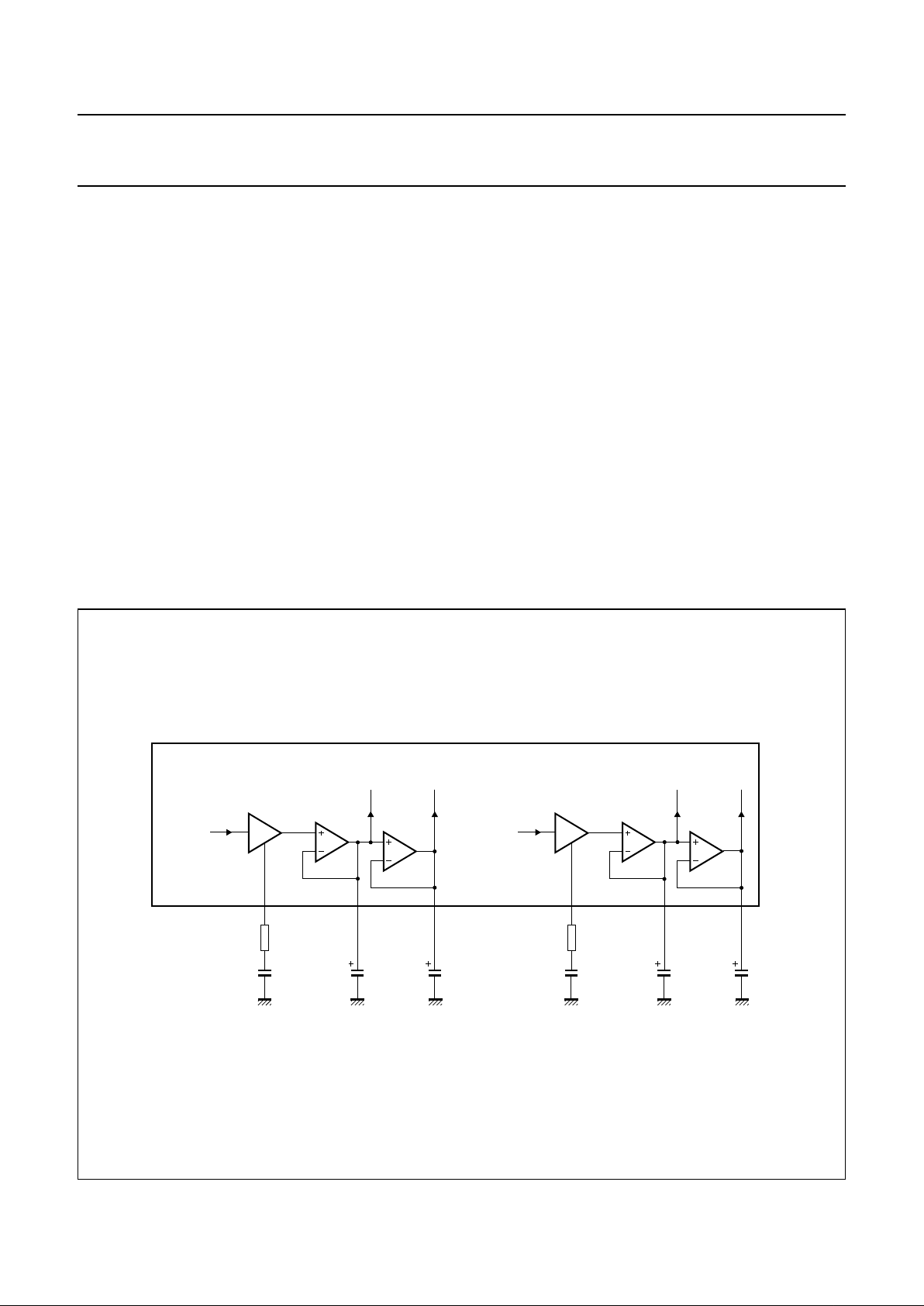
1997 Nov 25 9
Philips Semiconductors Product specification
Voice switched speakerphone IC TEA1095
The capacitors connected in series with the two resistors
block any DC component and form a first order high-pass
filter. In the basic application (see Fig.12), it is assumed
that V
TXIN
= 1 mV (RMS) and V
RXIN
= 100 mV (RMS)
nominal and both R
TSEN
and R
RSEN
have a value of 10 kΩ.
With the value of C
TSEN
and C
RSEN
at 100 nF, the cut-off
frequency is at 160 Hz.
The buffer amplifiers leading the compressed signals to
TENV and RENV have a maximum source current of
120 µA and a maximum sink current of 1 µA. Together with
the capacitors C
TENV
and C
RENV
, the timing of the signal
envelope monitors can be set. In the basic application, the
value of both capacitors is 470 nF. Because of the
logarithmic compression, each 6 dB signal increase
means 18 mV increase of the voltage on the envelopes
TENV or RENV at room temperature. Thus, timings can be
expressed in dB/ms. At room temperature, the 120 µA
sourced current corresponds to a maximum rise-slope of
the signal envelope of 85 dB/ms. This is enough to track
normal speech signals. The 1 µA current sunk by TENV or
RENV corresponds to a maximum fall-slope of 0.7 dB/ms.
This is enough for a smooth envelope and also eliminates
the effect of echoes on switching behaviour.
To determine the noise level, the signal on TENV and
RENV are buffered to TNOI and RNOI. These buffers have
a maximum source current of 1 µA and a maximum sink
current of 120 µA. Together with the capacitors C
TNOI
and
C
RNOI
, the timing can be set. In the basic application of
Fig.12, the value of both capacitors is 4.7 µF. At room
temperature, the 1 µA sourced current corresponds to a
maximum rise-slope of the noise envelope of
approximately 0.07 dB/ms. This is small enough to track
background noise and not to be influenced by speech
bursts. The 120 µA current that is sunk corresponds to a
maximum fall-slope of approximately 8.5 dB/ms. However,
during the decrease of the signal envelope, the noise
envelope tracks the signal envelope so it will never fall
faster than approximately 0.7 dB/ms. The behaviour of the
signal envelope and noise envelope monitors is illustrated
in Fig.7.
Fig.6 Signal and noise envelope detectors.
handbook, full pagewidth
MBG355
LOG LOG
from
transmit
amplifier
from
receiver
amplifier
DUPLEX CONTROLLER
TSEN
R
TSEN
C
TSEN
C
TENV
C
TNOI
R
RSEN
C
RSEN
C
RENV
C
RNOI
TENV TNOI RSEN RENV RNOI
to logicto logic
 Loading...