

Philips TEA1069AH Datasheet

INTEGRATED CIRCUITS
DATA SH EET
TEA1069; TEA1069A
Versatile speech/dialler/ringer with
music-on-hold
Product specification
Supersedes data of 1996 Dec 10
File under Integrated Circuits, IC03
1998 Jan 08

Philips Semiconductors Product specification
Versatile speech/dialler/ringer with
music-on-hold
FEATURES
Speech part
• Voltage regulator with adjustable static resistance
• Low DC line voltage; operates down to 1.6 V
(excluding polarity guard)
• Supply for dialler part and peripherals (not stabilized)
• Symmetrical high-impedance inputs (64 kΩ) for
dynamic, magnetic, or piezoelectric microphones
• Asymmetrical high-impedance input (32 kΩ) for electret
microphones
• Asymmetrical earpiece output for dynamic, magnetic,
or piezoelectric earpieces
• Internal mute to disable speech during dialling
• Confidence tone during DTMF dialling
• Line-loss compensation (line-current dependent) for
microphone and earpiece amplifiers
• Gain-control curve adaptable to the exchange supply.
Dialler part
• Pulse/DTMF and mixed mode dialling
• Last Number Redial (LNR), up to 32 digits
• 13 repertory numbers (3 direct and 10 indirect) or
10 repertory numbers (10 direct), up to 32 digits,
with a maximum of 224 digits in total
• Repertory and redial memory integrity check
(memory contents check)
• Notepad memory function
• Flash and earth register recall
• Dial mode output
• Access pause generation and termination
• Function keys for: store, memory recall, register recall,
LNR, pause, hold, mute, hook
• Keytone generation
• Hands-free control
• Volume control in hands-free mode (VOL+/VOL−)
• Hold function
• Mute function
• Music-on-hold
• Diode options:
– DTMF tone burst/pause time
– make/break ratio
– access pause time
TEA1069; TEA1069A
– pulse or DTMF mode selection
– register recall (earth and flash times)
– keyboard layout selection
– selection for german requirements
– hold/mute mode selection.
Ringer part
• Ringer input frequency discrimination
• Ringer melody generation (3-tone)
• Ringer melody selection/volume control via keyboard
• Diode option: ringer frequency selection.
GENERAL DESCRIPTION
The TEA1069 and TEA1069A contain all the functions
needed to build a highly featured, high-performance fully
electronic telephone set.
The device incorporates a speech/transmission part, a
dialler part and a ringer part. By offering a wide range of
possible adaptations for each part, the TEA1069 and
TEA1069A application can be easily adapted to meet
different requirements.
The TEA1069A offers some different timings and diode
options compared to the TEA1069.
Where pin numbers are mentioned in this data sheet we
refer to the TEA1069N, unless otherwise indicated.
Speech part
The speech/transmission part performs all speech and line
interface functions required in electronic sets. It operates
at line voltages down to 1.6 V DC to facilitate the use of
more telephones connected in parallel.
Dialler part
The dialler part offers a 32-digit Last Number Redial (LNR)
and 13 memories. Hands-free control is included allowing
the TEA1069 and TEA1069A to be used not only in basic
telephones, but also in feature phones offering hands-free
dialling via the TEA1083 call-progress monitor IC and/or
full hands-free operation via the TEA1093 hands-free IC.
The hold function allows the user to suspend the
conversation and resume the call either on the same
phone or on a parallel phone. Additionally through the
music-on-hold function a melody is transmitted while the
set is put on hold. The keytones provide in a buzzer an
audible feedback of a valid key pressed.
1998 Jan 08 2
Philips Semiconductors Product specification
Versatile speech/dialler/ringer with
TEA1069; TEA1069A
music-on-hold
Ringer part
The ringer part offers a discriminator input which enables the tone output as soon as a valid ring frequency is detected.
It offers a melody based on 3 tones with programmable melody and volume via keyboard.
ORDERING INFORMATION
TYPE
NUMBER
TEA1069N SDIP42 plastic shrink dual in-line package; 42 leads (600 mil) SOT270-1
TEA1069H QFP44 plastic quad flat package; 44 leads (lead length 1.3 mm);
TEA1069AH QFP44 plastic quad flat package; 44 leads (lead length 1.3 mm);
NAME DESCRIPTION VERSION
body 10 × 10 × 1.75 mm
body 10 × 10 × 1.75 mm
PACKAGE
SOT307-2
SOT307-2
1998 Jan 08 3
Philips Semiconductors Product specification
Versatile speech/dialler/ringer with
music-on-hold
BLOCK DIAGRAM
40
LN
38
AGCIRMUTEMOH/DMODP/FLKT/EARTH
6
36
CC
V
35
27
20
GAR
(40) 2
(36)
(34)
SPEECH
(44)
(32)
(31)
(22)
PULSE
(15)
(39) 1
RECEIVE
SECTION
QR
MUTE
GAS1
(37) 41
SECTION
TRANSMIT
HOLD
LOGIC
GAS2
(38) 42
dB
TEA1069
TEA1069A
SUPPLY
RINGER
TEA1069; TEA1069A
MBH195
(35)
39
SLPE
(43)
5
STAB
(33)
37
REG
(11, 18
and 23)
23
EE
V
(41)
3
MIC−
MIC+
DTMF
HOLD
DETECTOR/
GENERATOR
(42)
(1)
(16)
(17)
(21)
4
7
21
22
26
handbook, full pagewidth
Fig.1 Block diagram.
RECALL
8
(2)
KEY-
TONE
DETECTOR
KEYBOARD
TONE
DIALLER
34 (30)
33 (29)
32 (28)
31 (27)
30 (26)
29 (25)
14 (8)
15 (9)
16 (10)
17 (12)
18 (13)
COL6
COL5
COL4
COL3
ROW5
DIODE
ROW4
ROW3
ROW2
ROW1
COL2
1998 Jan 08 4
GENERATOR
19 (14)
9 (3)
CSI
COL1
10 (4)
XTAL1
TIMING/
CONTROL
11 (5)
12 (6)
XTAL2
13 (7)
CE/FDI
RESET
(19)
(24)
25 (20)
DD
V
24
28
HF TONE VOL1 VOL2
Pin numbers in parenthesis refer to the TEA1069H and TEA1069AH.
Philips Semiconductors Product specification
Versatile speech/dialler/ringer with
TEA1069; TEA1069A
music-on-hold
PINNING
SYMBOL
QR 1 39 receiving amplifier output
GAR 2 40 gain adjustment; receiving amplifier
MIC− 3 41 inverting microphone input
MIC+ 4 42 non-inverting microphone input
STAB 5 43 current stabilizer
IR 6 44 receiving amplifier input
DTMF 7 1 dual-tone multi-frequency input
KT/EARTH 8 2 keytone/earth recall output
CSI 9 3 cradle switch input
XTAL1 10 4 oscillator input
XTAL2 11 5 oscillator output
RESET 12 6 reset input
CE/FDI 13 7 chip enable/frequency discrimination input
COL6 14 8 keyboard column input 6
COL5 15 9 keyboard column input 5
COL4 16 10 keyboard column input 4
COL3 17 12 keyboard column input 3
COL2 18 13 keyboard column input 2
COL1 19 14 keyboard column input 1
DP/FL 20 15 dial pulse/flash output
HOLD 21 16 hold control input
VOL2 22 17 volume 2 output
V
EE
TONE 24 19 tone generator output
V
DD
VOL1 26 21 volume 1 output
MOH/DMO 27 22 music on hold/dial mode output
HF 28 24 hands-free control output
ROW1 29 25 keyboard row input/output 1
ROW2 30 26 keyboard row input/output 2
ROW3 31 27 keyboard row input/output 3
ROW4 32 28 keyboard row input/output 4
ROW5 33 29 keyboard row input/output 5
DIODE 34 30 diode option output
MUTE 35 31 mute output, active LOW
V
CC
REG 37 33 (DC) line voltage regulator decoupling
AGC 38 34 automatic gain control input
SOT270-1 SOT307-2
PIN
DESCRIPTION
23 11, 18, 23 negative line terminal
25 20 dialler/ringer part supply voltage
36 32 speech part supply voltage
1998 Jan 08 5
Philips Semiconductors Product specification
Versatile speech/dialler/ringer with
TEA1069; TEA1069A
music-on-hold
SYMBOL
SOT270-1 SOT307-2
SLPE 39 35 slope (DC resistance) adjustment
LN 40 36 positive line terminal
GAS1 41 37 gain adjustment; transmitting amplifier
GAS2 42 38 gain adjustment; transmitting amplifier
handbook, halfpage
QR
GAR
MIC−
MIC+
STAB
DTMF
KT/EARTH
CSI
XTAL1
XTAL2
RESET
CE/FDI
COL6
COL5
COL4
COL3
COL2
COL1
DP/FL
HOLD
IR
1
2
3
4
5
6
7
8
9
10
11
TEA1069N
12
13
14
15
16
17
18
19
20
PIN
MBH196
42
GAS2
41
GAS1
40
LN
39
SLPE
38
AGC
37
REG
V
36
35
MUTE
DIODE
34
33
ROW5
ROW4
32
31
ROW3
ROW2
30
29
ROW1
HF
28
27
MOH/DMO
VOL1
26
V
25
TONE
24
V
23
2221
VOL2
DESCRIPTION
CC
DD
EE
Fig.2 Pin configuration (SOT270-1).
1998 Jan 08 6
Philips Semiconductors Product specification
Versatile speech/dialler/ringer with
music-on-hold
IR
STAB
handbook, full pagewidth
DTMF
KT/EARTH
CSI
XTAL1
XTAL2
RESET
CE/FDI
COL6
COL5
COL4
V
EE
44
1
2
3
4
5
6
7
8
9
10
11
MIC+
43
42
MIC−
GARQRGAS2
41
40
TEA1069H
TEA1069AH
TEA1069; TEA1069A
GAS1LNSLPE
39
38
37
36
AGC
35
34
33
REG
V
32
CC
MUTE
31
DIODE
30
29
ROW5
ROW4
28
ROW3
27
ROW2
26
ROW1
25
HF
24
V
23
EE
12
13
14
15
COL3
COL2
COL1
DP/FL
Fig.3 Pin configuration (SOT307-2).
FUNCTIONAL DESCRIPTION
Speech part
For numbering of components refer to Figs 28 and 29.
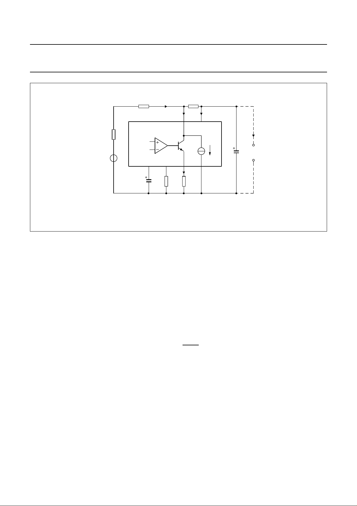
SUPPLIES VCC, LN, SLPE, REG AND STAB
Power for the IC and its peripheral circuits is usually
obtained from the telephone line (see Fig.4).
The circuit creates a stabilized voltage (V
= 3.7 V)
ref
between LN and SLPE. This reference voltage is
temperature compensated and can be adjusted by means
of an external resistor RVA. It can be increased by
connecting an RVA resistor (R60) between REG and SLPE
or decreased by connecting an RVA resistor (R61)
between REG and LN. This internal voltage reference is
decoupled by capacitor C3 between REG and VEE.
16
17
18
19
20
21
22
MBH784
HOLD
VOL2
EE
V
TONE
DD
V
VOL1
MOH/DMO
This decoupling capacitor realises the set impedance
conversion from its DC value to its AC value in the audio
frequency range.
The internal transmission part of the circuitry (including the
earpiece amplifier) is supplied from V
. This voltage
CC
supply is derived from the LN voltage via a dropping
resistor (R1) and must be decoupled by a capacitor (C1)
between VCC and VEE. This supply point may also be used
to supply the dialler/ringer (VDD) part or external circuit e.g.
electret microphone.
The DC current flowing into the set is determined by the
exchange supply voltage V
resistance R
line R
. When the line current (I
line
and the DC resistance of the telephone
exch
, the feeding bridge
exch
) is more than 0.5 mA
line
greater than the sum of the IC supply current (ICC) and the
current drawn by the peripheral circuitry connected to V
(Ip), the excess current is shunted to SLPE via LN.
CC
1998 Jan 08 7
Philips Semiconductors Product specification
Versatile speech/dialler/ringer with
music-on-hold
handbook, full pagewidth
V
R
exch
exch
R
line
I
TEA1069
TEA1069A
DC
AC
Fig.4 Supply arrangement.
I
line
+ 0.5 mA
SLPE
LN
SLPESTABREG
I
SLPE
C3 R5 R9
R1
V
I
CC
CC
0.5 mA
V
EE
TEA1069; TEA1069A
I
p
peripheral
C1
circuits
MBH197
Thus, the regulated voltage on the line terminal (VLN) can
be calculated as:
V
I
V
V
LN
SLPEIlineICCIp
ref
refISLPE
–=
is the internally generated temperature compensated
R9×+=
, where
0.5 103–A×++
reference voltage of 3.7 V and R9 is an external resistor
connected between SLPE and V
EE
.
The circuit has an internal current stabilizer operating at a
level determined by resistor R5 connected between STAB
and V
EE
.
In normal use the value of R5 would be 3.6 kΩ and the
value of R9 would be 20 Ω.
Changing the value of R5 or R9 will affect microphone
gain, DTMF gain, gain control characteristics, sidetone
level, maximum output swing on LN and the DC
characteristics (especially at low line current).
At line currents below 9 mA the internal reference voltage
is automatically adjusted to a lower value (typically 1.6 V
at 1 mA). This means that more sets can be operated in
parallel with DC line voltages (excluding the polarity guard)
down to an absolute minimum voltage of 1.6 V. At line
currents below 9 mA the circuit has limited sending and
receiving levels.
Under normal conditions, when I
>> ICC+ 0.5 mA + Ip,
SLPE
the static behaviour of the circuit is that of a 3.7 V regulator
diode (V
) with an internal resistance equal to that of R9.
ref
In the audio frequency range the dynamic impedance is
largely determined by R1. Figure 5 shows the equivalent
impedance of the circuit.
Current (Ip) available from VCC for the dialler part and
peripheral circuits depends on the external components
used. Figure 6 shows this current for VCC> 2.2 V. When
MUTE is HIGH i.e. when the receiving amplifier (supplied
from VCC) is driven, the available current is further
reduced. Current availability can be increased by
connecting the supply IC TEA1081 in parallel with R1, or
by increasing the DC line voltage by means of an external
resistor (RVA= R60) connected between REG and SLPE.
1998 Jan 08 8
Philips Semiconductors Product specification
Versatile speech/dialler/ringer with
music-on-hold
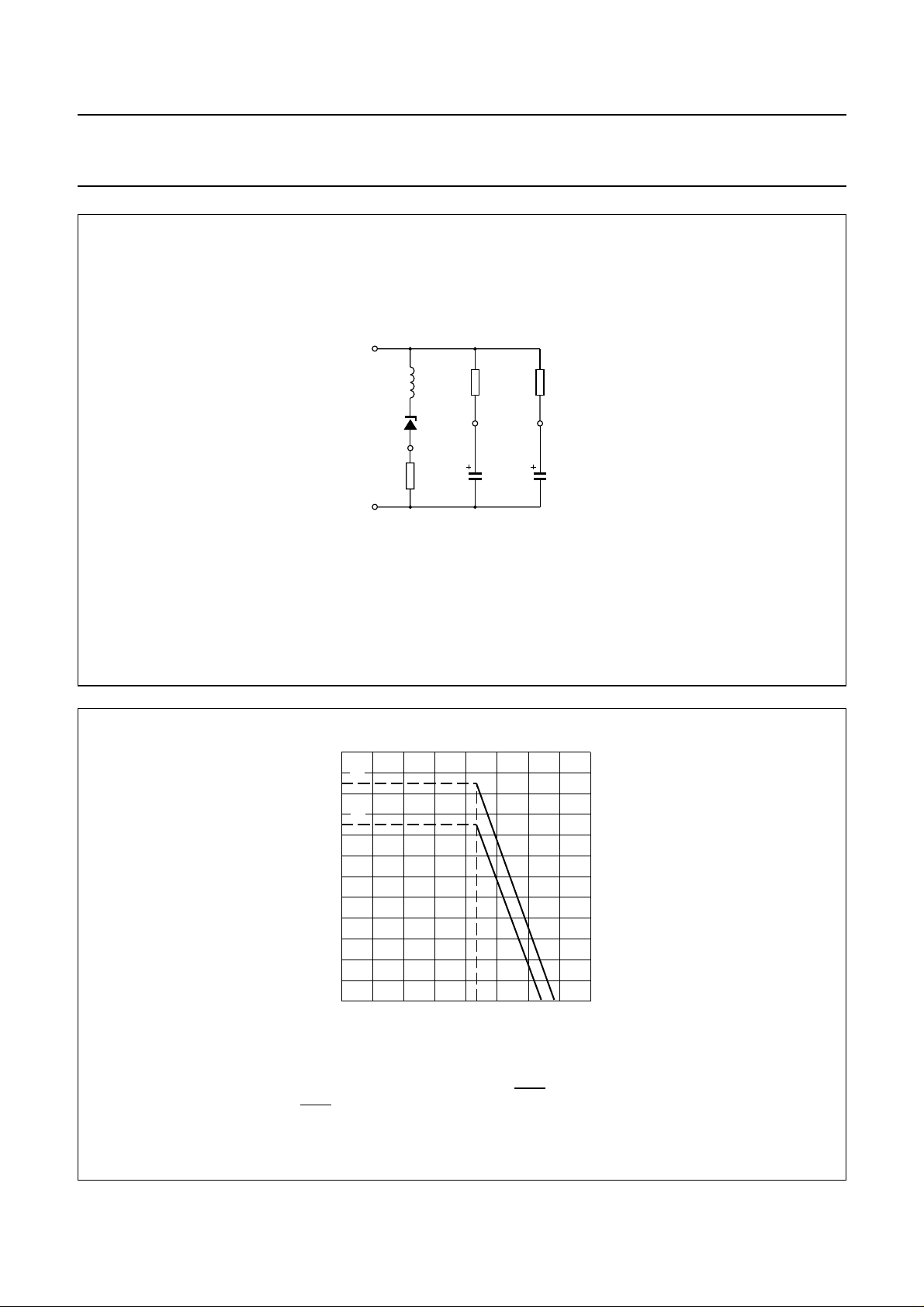
handbook, halfpage
LN
SLPE
V
EE
L
eq
V
R9
20 Ω
ref
R
REG
p
C3
4.7 µF C1100 µF
R1
V
CC
MGD489
TEA1069; TEA1069A
Leq=C3×R9 × Rp.
Rp= 16.2 kΩ.
Fig.5 Equivalent impedance circuit.
2.4
handbook, halfpage
(1)
I
p
(mA)
(2)
1.6
0.8
0
012 4
3
MSA504
VCC(V)
VCC> 2.2 V; I
(1) Ip= 2.1 mA. The curve is valid when the receiving amplifier is not driven or when MUTE = LOW.
(2) Ip= 1.7 mA. The curve is valid when MUTE = HIGH and the receiving amplifier is driven; V
= 15 mA at VLN= 4 V; R1 = 620 Ω; R9 = 20 Ω.
line
Fig.6 Typical current IP available from VCC for peripheral circuitry.
1998 Jan 08 9
= 150 mV, RL= 150 Ω.
o(rms)
Philips Semiconductors Product specification
Versatile speech/dialler/ringer with
TEA1069; TEA1069A
music-on-hold
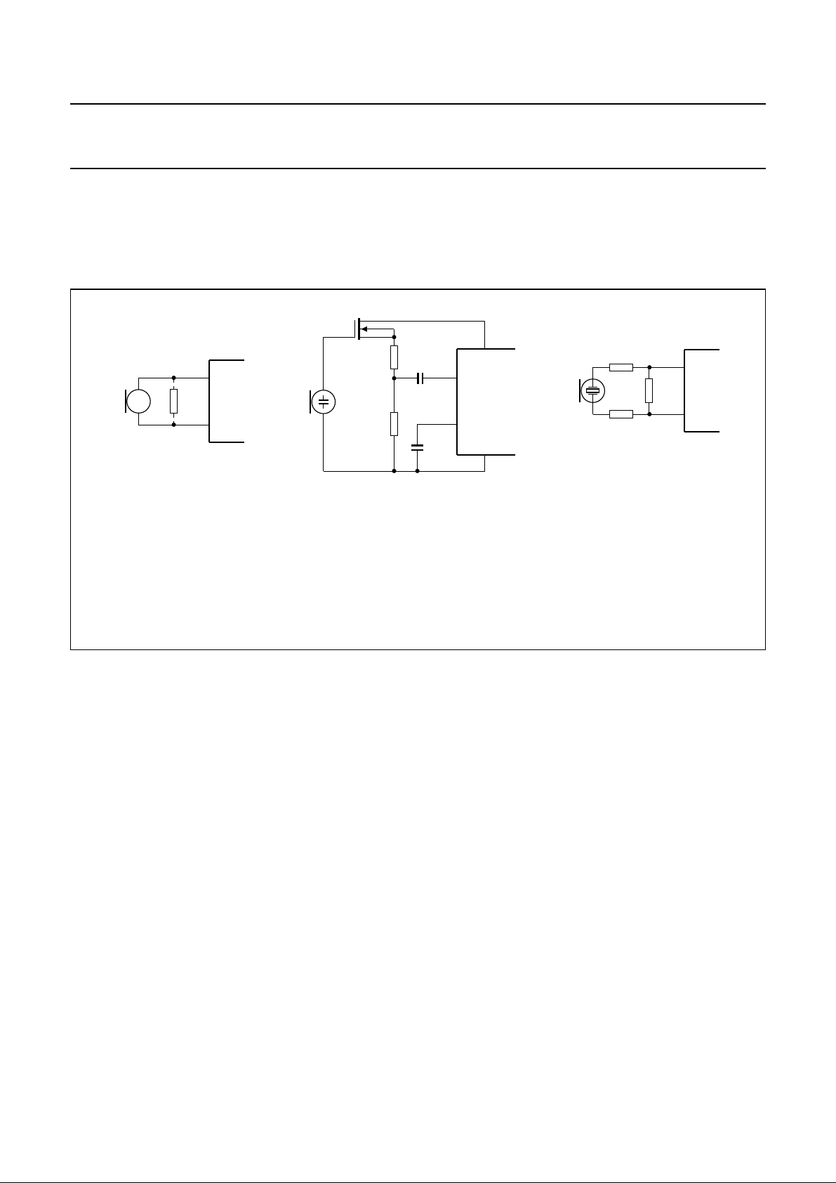
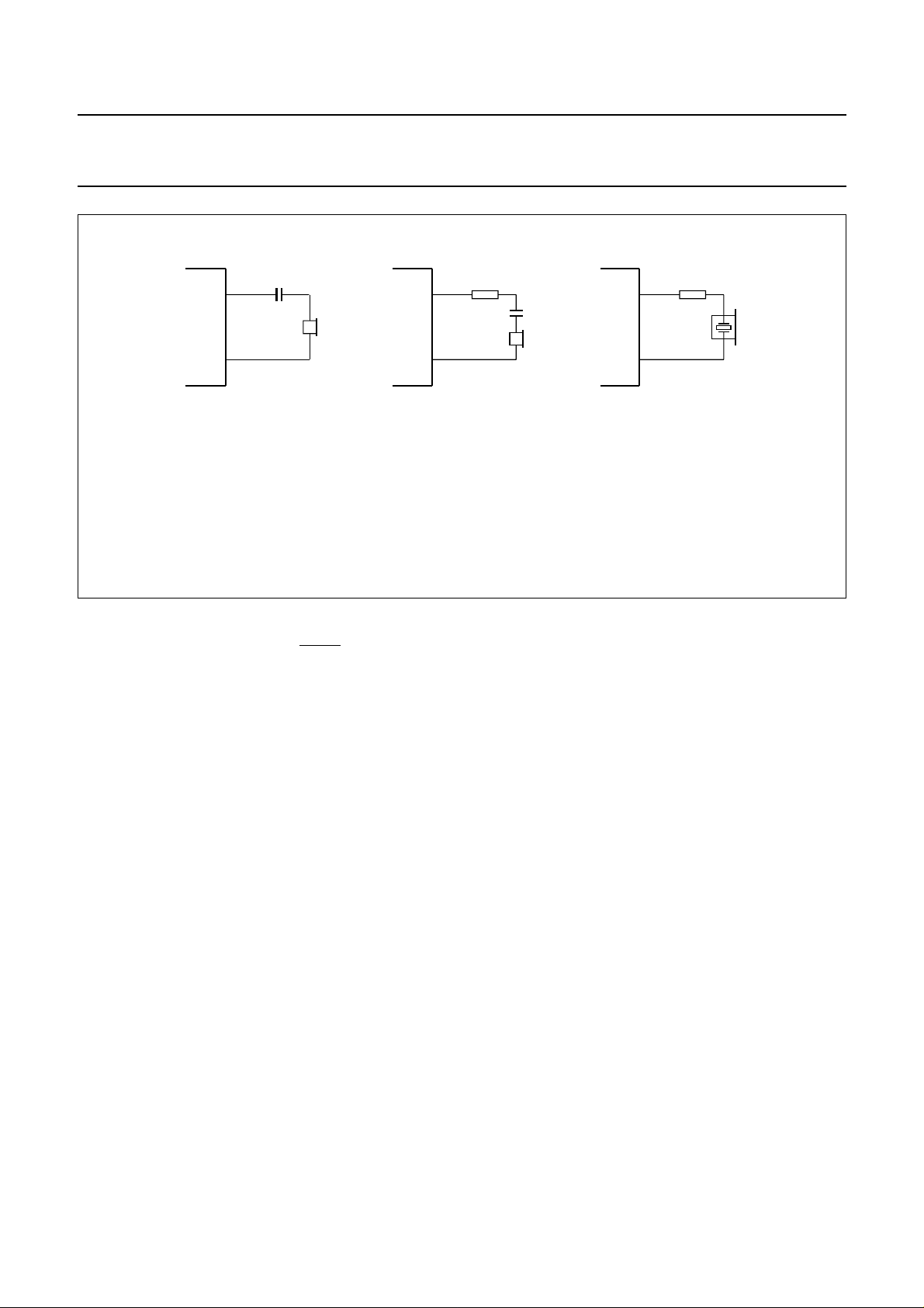
MICROPHONE INPUTS MIC+ AND MIC− AND GAIN PINS GAS1 AND GAS2
The circuit has symmetrical microphone inputs. Its input impedance is 64 kΩ (2 × 32 kΩ) and its voltage gain is typically
52 dB (when R7 = 68 kΩ). Dynamic, magnetic, piezoelectric or electret (with built-in FET source followers) microphones
can be used. Microphone arrangements are illustrated in Fig.7.
handbook, full pagewidth
36 (32)
V
4 (42)
MIC+
(1)
3 (41)
MIC−
a. Magnetic or dynamic
microphone.
3 (41)
MIC−
4 (42)
MIC+
b. Electret microphone.
CC
V
EE
23 (18)
c. Piezoelectric microphone.
4 (42)
3 (41)
MIC+
MIC−
MBH198
Pin numbers in parenthesis refer to the TEA1069H and TEA1069AH.
(1) Resistor may be connected to reduce the terminating impedance.
Fig.7 Alternative microphone arrangements.
The gain of the microphone amplifier can be adjusted
between 44 dB and 52 dB to suit the sensitivity of the
transducer in use. The gain is proportional to the value of
R7 which is connected between GAS1 and GAS2. Stability
is ensured by two external capacitors, C6 connected
between GAS1 and SLPE and C17 connected between
GAS1 and VEE. The value of C6 is 100 pF but this may be
increased to obtain a first-order low-pass filter. The value
of C17 is 10 times the value of C6. The cut-off frequency
corresponds to the time constant R7 × C6.
ECEIVING AMPLIFIER IR, QR AND GAR
R
The receiving amplifier has one input (IR) and one output
(QR). Earpiece arrangements are illustrated in Fig.8.
The IR to QR gain is typically 31 dB (when R4 = 100 kΩ).
It can be adjusted between 20 and 31 dB to match the
sensitivity of the transducer in use.
The gain is set with the value of R4 which is connected
between GAR and QR. The overall receive gain, between
LN and QR, is calculated by subtracting the anti-sidetone
network attenuation (32 dB) from the amplifier gain.
Two external capacitors, C4 and C7, ensure stability. C4 is
normally 100 pF and C7 is 10 times the value of C4.
The value of C4 may be increased to obtain a first-order
low-pass filter. The cut-off frequency will depend on the
time constant R4 × C4.
The output voltage of the receiving amplifier is specified for
continuous-wave drive. The maximum output voltage will
be higher under speech conditions where the peak to RMS
ratio is higher.
1998 Jan 08 10
Philips Semiconductors Product specification
k
Versatile speech/dialler/ringer with
music-on-hold
, full pagewidth
1 (39)
QR
23 (18)
V
EE
a. Dynamic earpiece. b. Magnetic earpiece. c. Piezoelectric earpiece.
Pin numbers in parenthesis refer to the TEA1069H and TEA1069AH.
(1) Resistor may be connected to prevent distortion (inductive load).
(2) Resistor is required to increase the phase margin (capacitive load).
Fig.8 Alternative receiver arrangements.
(1) (2)
1 (39)
QR QR
23 (18)
V
EE
TEA1069; TEA1069A
1 (39)
23 (18)
V
EE
MBH199
DUAL TONE MULTI-FREQUENCY INPUT DTMF
When the DTMF input is enabled (MUTE is LOW) dialling
tones may be sent on to the line. The voltage gain from
DTMF to LN is typically 25.5 dB (when R7 = 68 kΩ) and
varies with R7 in the same way as the microphone gain.
The tones can be heard in the earpiece at a low level
(confidence tone).
microphone amplifier and the receiving amplifier in
accordance with the DC line current.
The control range is 5.8 dB which corresponds to a line
length of 5 km for a 0.5 mm diameter twisted-pair copper
cable with a DC resistance of 176 Ω/km and average
attenuation of 1.2 dB/km. Resistor R6 should be chosen in
accordance with the exchange supply voltage and its
feeding bridge resistance (see Fig.9 and Table 1).
A
UTOMATIC GAIN CONTROL INPUT AGC
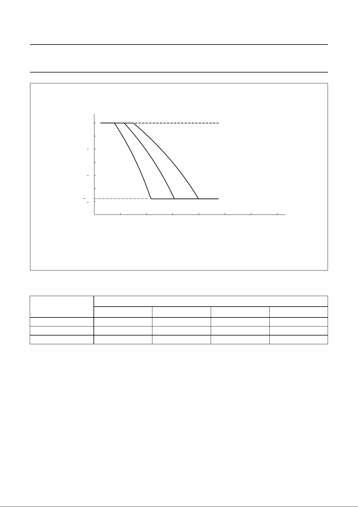
Automatic line loss compensation is achieved by
connecting a resistor (R6) between AGC and VEE.
The automatic gain control varies the gain of the
The ratio of start and stop currents of the AGC curve is
independent of the value of R6. If no automatic line-loss
compensation is required the AGC pin may be left
open-circuit. The amplifiers, in this condition, will give their
maximum specified gain.
1998 Jan 08 11
Philips Semiconductors Product specification
Versatile speech/dialler/ringer with
music-on-hold
handbook, full pagewidth
0
∆G
v
(dB)
2
5.8
4
6
78.7 kΩ
R6 = ∞
110 kΩ 140 kΩ
TEA1069; TEA1069A
MGD490
I (mA)
140120100806040200
line
Fig.9 Variation of gain as function of line current with R6 as parameter.
Table 1 Values of resistor R6 for optimum line-loss compensation at various values of exchange supply voltage
(V
) and exchange feeding bridge resistance (R
exch
); R9 = 20 Ω
exch
R6 (kΩ)
V
(V)
exch
R
= 400 Ω R
exch
= 600 Ω R
exch
= 800 Ω R
exch
exch
= 1000 Ω
36 100 78.7 −−
48 140 110 93.1 82
60 −−120 102
1998 Jan 08 12
Philips Semiconductors Product specification
Versatile speech/dialler/ringer with
music-on-hold
SIDETONE SUPPRESSION
Suppression of the transmitted signal in the earpiece is
obtained by the anti-sidetone network comprising R1//Z
R2, R3, R8, R9 and Z
(see Fig.10). The maximum
bal
compensation is obtained when the following conditions
are fulfilled:
R9 R2× R1 R3 R8+()×=
kR3
Z
bal
R8 R9+()
×=
----------------------------R2 R9×()
kZ
×=
line
The scale factor k is chosen to meet the compatibility with
a standard capacitor from the E6 or E12 series for Z
In practice, Z
length. Therefore, the value chosen for Z
varies considerably with the line type and
line
should be for
bal
an average line length thus giving optimum setting for
short or long lines.
Example: the balance impedance Z
at which the
bal
optimum suppression is present can be calculated as
line
line
(1)
(2)
(3)
.
TEA1069; TEA1069A
follows:
suppose Z
5 km line of 0.5 mm diameter, copper, twisted-pair cable
,
matched to 600 Ω (176 Ω/km; 38 nF/km).
When k = 0.64 then R8 = 390 Ω;
Z
= 130 Ω + (820 Ω//220 nF).
bal
The anti-sidetone network for the TEA1069 and
TEA1069A shown in Fig.10 attenuates the signal received
from the line by 32 dB before it enters the receiving
amplifier.
The attenuation is almost constant over the whole
audio-frequency range. Figure 11 shows a conventional
Wheatstone bridge anti-sidetone circuit that can be used
as an alternative. Both bridge types can be used with
either resistive or complex set impedances. More
information on the balancing of anti-sidetone bridges can
be found in our publication
Wired telecom systems, IC03b”
9397 750 00811.
= 210 Ω + (1265 Ω//140 nF) representing a
line
“Applications Handbook for
, order number
handbook, full pagewidth
LN
Z
line
V
EE
R1 R2
i
m
R9
R8
SLPE
R3
IR
R
t
Z
bal
MSA500 - 1
Fig.10 Equivalent circuit of TEA1069 and TEA1069A anti-sidetone bridge.
1998 Jan 08 13
Philips Semiconductors Product specification
Versatile speech/dialler/ringer with
music-on-hold
handbook, full pagewidth
Z
line
V
EE
Fig.11 Equivalent circuit of an anti-sidetone network in a Wheatstone bridge configuration.
Dialler and ringer part
UPPLY VOLTAGE: PINS VDDAND V
S
EE
The power supply must be maintained for data storage.
The RAM retention voltage (standby supply voltage) may
drop down to 1.0 V. Applying a large capacitor across the
supply terminals can retain the memory if power
connections are broken. The minimum operation voltage is
2.5 V. The internal power-on reset is enabled for a voltage
below this minimum operation voltage.
O
SCILLATOR INPUT/OUTPUT: PINS XTAL1AND XTAL2
Time base for the TEA1069 and TEA1069A is a
crystal-controlled on-chip oscillator which is completed by
connecting a 3.579545 MHz crystal or ceramic resonator
between XTAL1 and XTAL2. The oscillator starts when
VDD reaches the operation voltage level and
CE/FDI = HIGH. The following types of ceramic
resonators are recommended:
• Kyocera PBRC3.58ARPC10 (wired)
• Kyocera KBR3.58MSATRPC10 (SMD)
• Murata CSA3.58MG310VA (wired).
R
ESET INPUT: PIN RESET
Pin RESET is an input to the internal reset circuit. When
RESET = HIGH, it can be used to initialize the TEA1069
and TEA1069A which is normally done by the CE/FDI
input. The on-chip power-on reset generates a reset pulse
if VDD drops below 2.5 V. In this event a proper start-up
R1
R9
TEA1069; TEA1069A
LN
Z
bal
i
m
R8
SLPE
occurs after the supply voltage rises above the minimum
operation voltage level again.
During and directly after reset pins 14 to 19, 21, 29 to 32,
34 and 35 are set HIGH; pins 8, 20, 22, 26 to 28 and 33
are set to LOW.
The RESET pin can be connected to V
resistor of 100 kΩ to 1 MΩ, which will save leakage
current. A capacitor connected to VDD can be used to
extend the reset time, in case a longer reset is desirable.
To prevent the dialler from reacting on voltage
disturbances on the telephone line a time-out is active.
The dialler returns to standby state if the voltage on the line
has disappeared for more than this reset-delay time (trd).
C
HIP ENABLE/FREQUENCY DISCRIMINATOR INPUT:
PIN CE/FDI
This active HIGH input is used to initialize part of the
system, to select the on-line, standby, or ringer mode and
to detect line power breaks. To keep the TEA1069 and
TEA1069A in the on-line mode, CE/FDI has to be HIGH.
In the exchange, several AC signals can be superimposed
on the DC signal, e.g. dialling tone, busy tone,
disturbances (like line power breaks), and the ringer
signal. The ringer signal is evaluated, and checked if its
frequency is within the limits of the frequency interval as
set by the diode option RFS. It is assumed that the ringer
frequency at pin CE/FDI is the double of the frequency
present on the telephone line.
IR
R
t
R
A
MSA501 - 1
, preferably via a
EE
1998 Jan 08 14
 Loading...