

Philips TEA1067T, TEA1067 Datasheet

INTEGRATED CIRCUITS
DATA SH EET
TEA1067
Low voltage versatile telephone
transmission circuit with dialler
interface
Product specification
File under Integrated Circuits, IC03A
June 1990
Philips Semiconductors Product specification
Low voltage versatile telephone
transmission circuit with dialler interface
GENERAL DESCRIPTION
The TEA1067 is a bipolar integrated circuit performing all
speech and line interface functions required in fully
electronic telephone sets. It performs electronic switching
between dialling and speech. The circuit is able to operate
down to a DC line voltage of 1.6 V (with reduced
performance) to facilitate the use of more telephone sets
in parallel.
Features
• Low DC line voltage; operates down to 1.6 V (excluding
polarity guard)
• Voltage regulator with adjustable static resistance
• Provides supply with limited current for external circuitry
• Symmetrical high-impedance inputs (64 kΩ) for
dynamic, magnetic or piezoelectric microphones
QUICK REFERENCE DATA
• Asymmetrical high-impedance input (32 kΩ) for electret
• DTMF signal input with confidence tone
• Mute input for pulse or DTMF dialling
• Power down input for pulse dial or register recall
• Receiving amplifier for magnetic, dynamic or
• Large gain setting range on microphone and earpiece
• Line current dependent line loss compensation facility
• Gain control adaptable to exchange supply
• DC line voltage adjustment capability
TEA1067
microphone
piezoelectric earpieces
amplifiers
for microphone and earpiece amplifiers
PARAMETER CONDITIONS SYMBOL MIN. TYP. MAX. UNIT
Line voltage I
= 15 mA V
line
Line current operating range normal operation
TEA1067 I
TEA1067T I
with reduced performance I
Internal supply current power down
input LOW I
input HIGH I
Supply voltage for peripherals I
= 15 mA; Ip= 1.4 mA;
line
mute input HIGH V
= 15 mA; Ip= 0.9 mA;
I
line
mute input HIGH V
Voltage gain range
microphone amplifier G
receiving amplifier G
Line loss compensation
gain control range ∆G
Exchange supply voltage range V
Exchange feeding bridge
resistance range R
line
line
line
CC
CC
LN
CC
CC
v
v
v
exch
exch
3.65 3.9 4.15 V
11 − 140 mA
11 − 140 mA
1 − 11 mA
− 1 1.35 mA
− 55 82 µA
2.2 2.4 − V
2.5 −− V
44 − 52 dB
20 − 45 dB
5.5 5.9 6.3 dB
36 − 60 V
0.4 − 1kΩ
PACKAGE OUTLINES
TEA1067: 18-lead DIL; plastic (SOT102). SOT102-1; 1998 Jun 18.
TEA1067T: 20-lead mini-pack; plastic (SO20; SOT163A). SOT163-1; 1998 Jun 18.
June 1990 2
Philips Semiconductors Product specification
Low voltage versatile telephone
transmission circuit with dialler interface
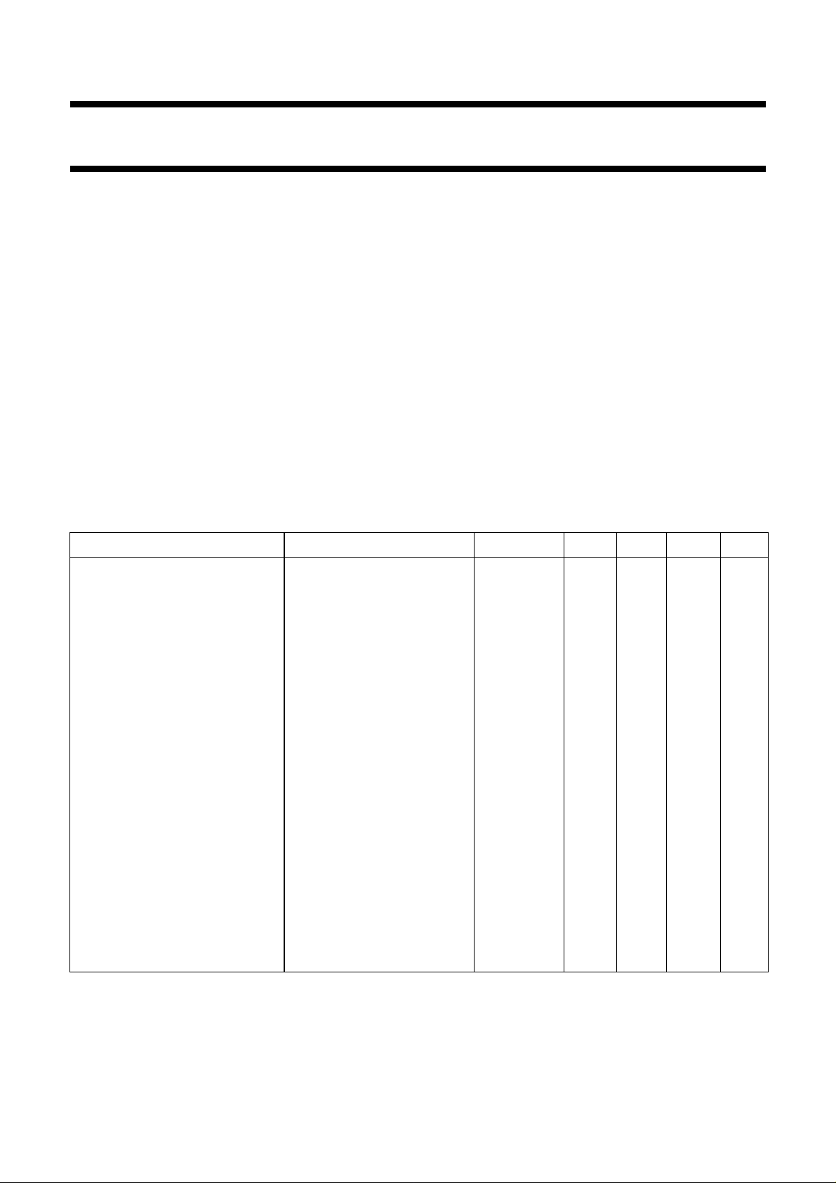
handbook, full pagewidth
MIC+
MIC−
DTMF
MUTE
PD
11 (12)
IR
8 (9)
7 (7)
13 (15)
14 (16)
12 (14)
V
CC
15 (17)
TEA1067
TEA1067T
+−+
(1)
dB
dB
SUPPLY AND
REFERENCE
+
−
−
+
−
CIRCUIT
AGC
−
+
−
+
−
+
LOW
VOLTAGE
CIRCUIT
(1)1
LN
(6) 6
(5) 5
(4) 4
(2) 2
(3) 3
TEA1067
GAR
QR+
QR−
GAS1
GAS2
V
EE
Figures in parenthesis refer to TEA1067T.
CURRENT
REFERENCE
16 (18)10 (11)
REG AGC STAB SLPE
17 (19) 9 (10) (20)18
Fig.1 Block diagram.
MGR082
June 1990 3
Philips Semiconductors Product specification
Low voltage versatile telephone
transmission circuit with dialler interface
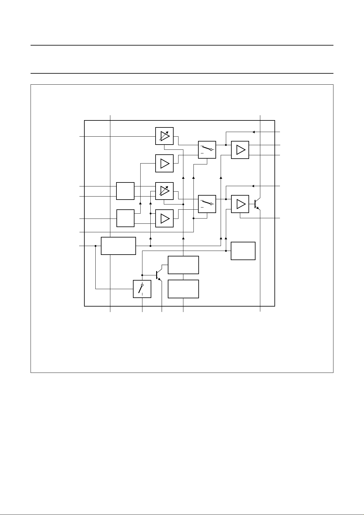
PINNING
handbook, halfpage
Fig.2 Pinning diagram for TEA1067 18-lead DIL
LN
GAS1
GAS2
QR−
QR+
GAR
MIC−
MIC+
STAB
version.
1
2
3
4
5
6
7
8
9
TEA1067
MGR084
SLPE
18
AGC
17
REG
16
V
15
CC
MUTE
14
DTMF
13
PD
12
IR
11
V
10
EE
TEA1067
1 LN positive line terminal
2 GAS1 gain adjustment; transmitting amplifier
3 GAS2 gain adjustment; transmitting amplifier
4QR− inverting output; receiving amplifier
5QR+ non-inverting output receiving amplifier
6 GAR gain adjustment; receiving amplifier
7 MIC− inverting microphone input
8 MIC+ non-inverting microphone input
9 STAB current stabilizer
10 V
EE
11 IR receiving amplifier input
12 PD power-down input
13 DTMF dual-tone multi-frequency input
14 MUTE mute input
15 V
CC
16 REG voltage regulator decoupling
17 AGC automatic gain control input
18 SLPE slope (DC resistance) adjustment
negative line terminal
positive supply decoupling
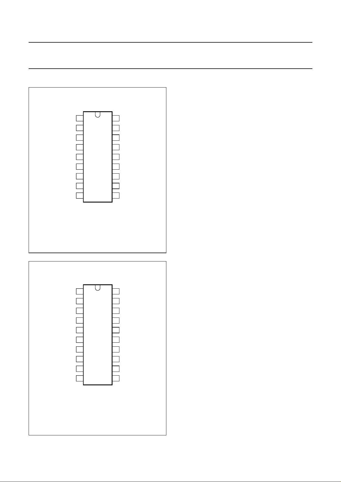
handbook, halfpage
LN
1
GAS1
2
GAS2
3
QR−
4
QR+
5
GAR
MIC−
n.c. n.c.
MIC+
STAB
TEA1067T
6
7
8
9
10
20
19
18
17
16
15
14
13
12
11
MGR083
SLPE
AGC
REG
V
CC
MUTE
DTMF
PD
IR
V
EE
Fig.3 Pinning diagram for TEA1067T 20-lead
mini-pack version.
1 LN positive line terminal
2 GAS1 gain adjustment; transmitting amplifier
3 GAS2 gain adjustment; transmitting amplifier
4QR− inverting output; receiving amplifier
5QR+ non-inverting output receiving amplifier
6 GAR gain adjustment, receiving amplifier
7 MIC− inverting microphone input
8 n.c. not connected
9 MIC+ non-inverting microphone input
10 STAB current stabilizer
11 V
EE
negative line terminal
12 IR receiving amplifier input
13 n.c. not connected
14 PD power-down input
15 DTMF dual-tone multi-frequency input
16 MUTE mute input
17 V
CC
positive supply decoupling
18 REG voltage regulator decoupling
19 AGC automatic gain control input
20 SLPE slope (DC resistance) adjustment
June 1990 4

Philips Semiconductors Product specification
Low voltage versatile telephone
transmission circuit with dialler interface
FUNCTIONAL DESCRIPTION
Supply: V
Power for the TEA1067 and its peripheral circuits is usually
obtained from the telephone line. The IC develops its own
supply at V
voltage VCCmay also be used to supply external circuits
e.g. dialling and control circuits.
Decoupling of the supply voltage is performed by a
capacitor between VCCand VEEwhile the internal voltage
regulator is decoupled by a capacitor between REG and
VEE.
The DC current drawn by the device will vary in
accordance with varying values of the exchange voltage
(V
exch
resistance of the telephone line (R
The TEA1067 has an internal current stabilizer working at
a level determined by a 3.6 kΩ resistor connected
between STAB and VEE(see Fig.7). When the line current
(I
) is more than 0.5 mA greater than the sum of the IC
line
supply current (ICC) and the current drawn by the
peripheral circuitry connected to VCC(Ip) the excess
current is shunted to VEEvia LN.
The regulated voltage on the line terminal (VLN) can be
calculated as:
VLN=V
VLN= V
Where V
compensated reference voltage of 3.6 V and R9 is an
external resistor connected between SLPE and VEE.
, LN, SLPE, REG and STAB
CC
and regulates its voltage drop. The supply
CC
), the feeding bridge resistance (R
).
line
ref
ref
+ I
+ [(I
ref
× R9; or
SLPE
− ICC− 0.5 × 10⁻³A) − Ip] × R9
line
is an internally generated temperature
), and the DC
exch
TEA1067
In normal use the value of R9 would be 20Ω. Changing the
value of R9 will also affect microphone gain, DTMF gain,
gain control characteristics, side-tone level and maximum
output swing on LN, and the DC characteristics (especially
at the lower voltages).
Under normal conditions, when I
the static behaviour of the circuit is that of a 3.6 V regulator
diode with an internal resistance equal to that of R9. In the
audio frequency range the dynamic impedance is largely
determined by R1. Fig.4 shows the equivalent impedance
of the circuit.
At line currents below 9 mA the internal reference voltage
is automatically adjusted to a lower value (typically 1.6 V
at 1 mA). This means that the operation of more sets in
parallel is possible with DC line voltages (excluding the
polarity guard) down to an absolute minimum voltage of
1.6 V. With line currents below 9 mA the circuit has limited
sending and receiving levels. The internal reference
voltage can be adjusted by means of an external resistor
(RVA). This resistor connected between LN and REG will
decrease the internal reference voltage, connected
between REG and SLPE it will increase the internal
reference voltage.
Current (Ip) available from VCCfor peripheral circuits
depends on the external components used. Fig.10 shows
this current for VCC> 2.2 V. If MUTE is LOW when the
receiving amplifier is driven the available current is further
reduced. Current availability can be increased by
connecting the supply IC (TEA1081) in parallel with R1, as
shown in Fig.17 (c), or by increasing the DC line voltage by
means of an external resistor (RVA) connected between
REG and SLPE.
>> ICC+ 0.5 mA + Ip,
SLPE
June 1990 5
Philips Semiconductors Product specification
Low voltage versatile telephone
transmission circuit with dialler interface
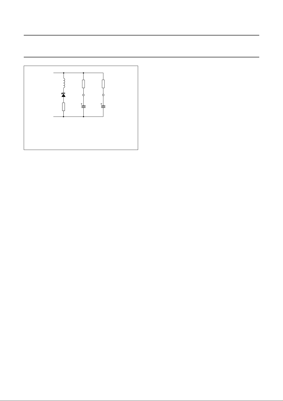
handbook, halfpage
Rp= 16.2 kΩ
L
eq
Microphone inputs (MIC+ and MIC−) and gain
adjustment pins (GAS1 and GAS2)
The TEA1067 has symmetrical microphone inputs. Its
input impedance is 64 kΩ (2 × 32 kΩ) and its voltage gain
is typically 52 dB (when R7 = 68 kΩ, see Fig.14). Dynamic,
magnetic, piezoelectric or electret (with built-in FET source
followers) microphones can be used. Microphone
arrangements are shown in Fig.11.
The gain of the microphone amplifier can be adjusted
between 44 dB and 52 dB to suit the sensitivity of the
transducer in use. The gain is proportional to the value of
R7 which is connected between GAS1 and GAS2. Stability
is ensured by the external capacitor C6 which is connected
between GAS1 and SLPE. The value of C6 is 100 pF but
this may be increased to obtain a first-order low-pass filter.
The cut-off frequency corresponds to the time constant
R7 × C6.
Mute input (MUTE)
When MUTE is HIGH the DTMF input is enabled and the
microphone and receiving amplifier inputs are inhibited.
The reverse is true when MUTE is LOW or open-circuit.
MUTE switching causes only negligible clicking on the
earpiece outputs and line. If the number of parallel sets in
use causes a drop in line current to below 6 mA the speech
amplifiers remain active independent to the DC level
applied to the MUTE input.
LN
V
EE
= C3 × R9 × R
L
eq
V
ref
R9
20 Ω
p
R
p
REG
C3
4.7 µF
MBA454
Fig.4 Equivalent impedance circuit.
R1
V
CC
C1
100 µF
TEA1067
Dual-tone multi-frequency input (DTMF)
When the DTMF input is enabled dialling tones may be
sent onto the line. The voltage gain from DTMF to LN is
typically 25.5 dB (when R7 = 68 kΩ) and varies with R7 in
the same way as the microphone gain. The signalling
tones can be heard in the earpiece at a low level
(confidence tone).
Receiving Amplifier (IR, QR+, QR− and GAR)
The receiving amplifier has one input (IR), one
non-inverting complementary output (QR+) and an
inverting complementary output (QR−). These outputs
may be used for single-ended or differential drive
depending on the sensitivity and type of earpiece used
(see Fig.12). IR to QR + gain is typically 31 dB (when
R4 = 100 kΩ), this is sufficient for low-impedance
magnetic or dynamic microphones which are suited for
single-ended drive. Using both outputs for differential drive
gives an additional gain of 6 dB. This feature can be used
when the earpiece impedance exceeds 450 Ω
(high-impedance dynamic or piezoelectric types).
The receiving amplifier gain can be adjusted between 20
and 39 dB with single-ended drive and between 26 and
45 dB with differential drive, to match the sensitivity of the
transducer in use. The gain is set with the value of R4
which is connected between GAR and QR+. Overall
receive gain between LN and QR+ is calculated by
substracting the anti-sidetone network attenuation (32 dB)
from the amplifier gain. Two external capacitors C4 and
C7, ensure stability. C4 is normally 100 pF and C7 is
10 × the value of C4. The value of C4 may be increased to
obtain a first-order low-pass filter. The cut-off frequency
will depend on the time constant R4 × C4.
The output voltage of the receiving amplifier is specified for
continuous-wave drive. The maximum output voltage will
be higher under speech conditions where the peak to RMS
ratio is higher.
June 1990 6

Philips Semiconductors Product specification
Low voltage versatile telephone
transmission circuit with dialler interface
Automatic gain control input (AGC)
Automatic line loss compensation is achieved by
connecting a resistor (R6) between AGC and VEE. The
automatic gain control varies the gain of the microphone
amplifier and the receiving amplifier in accordance with the
DC line current. The control range is 5.9 dB. This
corresponds to a line length of 5 km for a 0.5 mm diameter
copper twisted-pair cable with a DC resistance of
176 Ω/km and an average attenuation 1.2 dB/km. Resistor
R6 should be chosen in accordance with the exchange
supply voltage and its feeding bridge resistance (see
Fig.13 and Table 1). The ratio of start and stop currents of
the AGC curve is independent of the value of R6. If no
automatic line loss compensation is required the AGC may
be left open-circuit. The amplifiers, in this condition, will
give their maximum specified gain.
Power-down input (PD)
During pulse dialling or register recall (timed loop break)
the telephone line is interrupted. During these interruptions
the telephone line provides no power for the transmission
circuit or circuits supplied by V
will bridge these gaps. This bridging is made easier by a
HIGH level on the PD input which reduces the typical
supply current from 1 mA to 55 µA and switches off the
voltage regulator preventing discharge through LN. When
PD is HIGH the capacitor at REG is disconnected with the
effect that the voltage stabilizer will have no switch-on
delay after line interruptions. This minimizes the
contribution of the IC to the current waveform during pulse
dialling or register recall. When this facility is not required
PD may be left open-circuit.
. The charge held on C1
CC
TEA1067
Side-tone suppression
The anti-sidetone network, R1//Z
(see Fig.5) suppresses transmitted signal in the earpiece.
Compensation is maximum when the following conditions
are fulfilled:
(a) R9 × R2 = R1 (R3 + [R8//Z
(b) (Z
bal
/ [Z
+ R8]) = (Z
bal
line
/ [Z
If fixed values are chosen for R1, R2, R3, and R9 then
condition (a) will always be fulfilled whenR8//Z
To obtain optimum side-tone suppression condition (b)
has to be fulfilled resulting in:
Z
= (R8/R1) Z
bal
line
= k.Z
where k is a scale factor;
line
k = (R8/R1)
The scale factor (k), dependent on the value of R8, is
chosen to meet the following criteria:
(a) Compatibility with a standard capacitor from the E6 or
E12 range for Z
(b) Z
//R8 << R3 to fulfil condition (a) and thus
bal
bal
ensuring correct anti-sidetone bridge operation
(c) Z
+ R8 >> R9 to avoid influencing the transmitter
bal
gain
In practice Z
varies considerably with the line type and
line
length. The value chosen for Z
an average line length thus giving optimum setting for
short or long lines.
, R2, R3, R9 and Z
line
]);
bal
+ R1])
line
bal
should therefore be for
bal
bal
<< R3.
,
June 1990 7
Philips Semiconductors Product specification
Low voltage versatile telephone
transmission circuit with dialler interface
Example
The line balance impedance (Z
suppression is present can be calculated by:
suppose Z
= 210 Ω+ (1265 Ω//140 nF), representing a
line
5 km line of 0.5 mm diameter, copper, twisted-pair cable
matched to 600 Ω (176 Ω/km; 38 nF/km).
When k = 0.64 then R8 = 390 Ω;
Z
= 130 Ω+ (820 Ω//220 nF).
bal
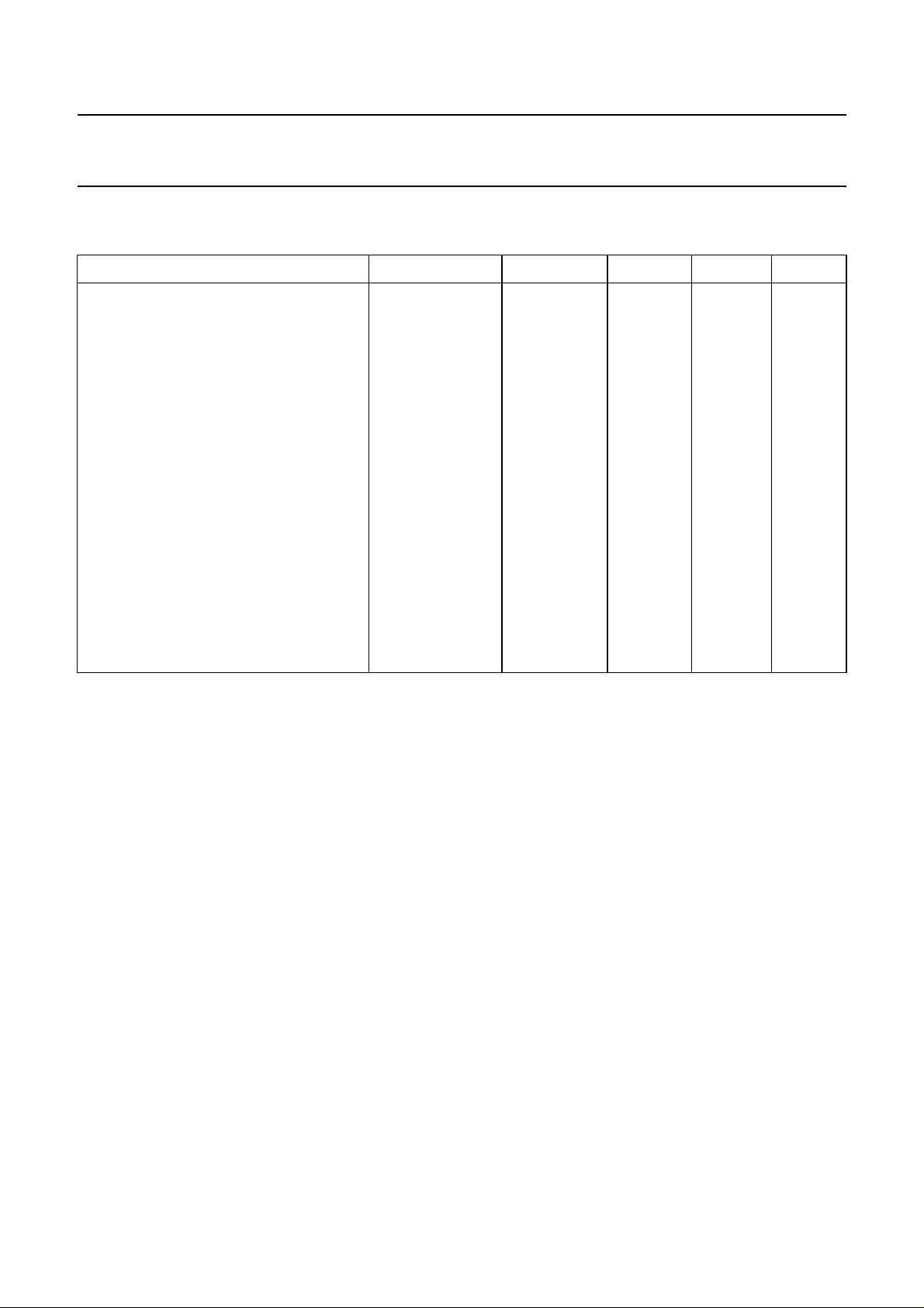
handbook, full pagewidth
) at which the optimum
bal
Z
line
V
R1
EE
R9
LN
SLPE
TEA1067
The anti-sidetone network for the TEA1060 family shown
in Fig.5 attenuates the signal received from the line by 32
dB before it enters the receiving amplifier. The attenuation
is almost constant over the whole audio frequency range.
Fig.6 shows a conventional Wheatstone bridge
anti-sidetone circuit that can be used as an alternative.
Both bridge types can be used with either resistive or
complex set impedances.
R2
i
m
R3
R8
IR
R
t
Z
bal
MSA500
Fig.5 Equivalent circuit of TEA1060 anti-sidetone bridge.
handbook, full pagewidth
Z
line
V
R1
EE
R9
LN
SLPE
Z
bal
i
m
R8
R
A
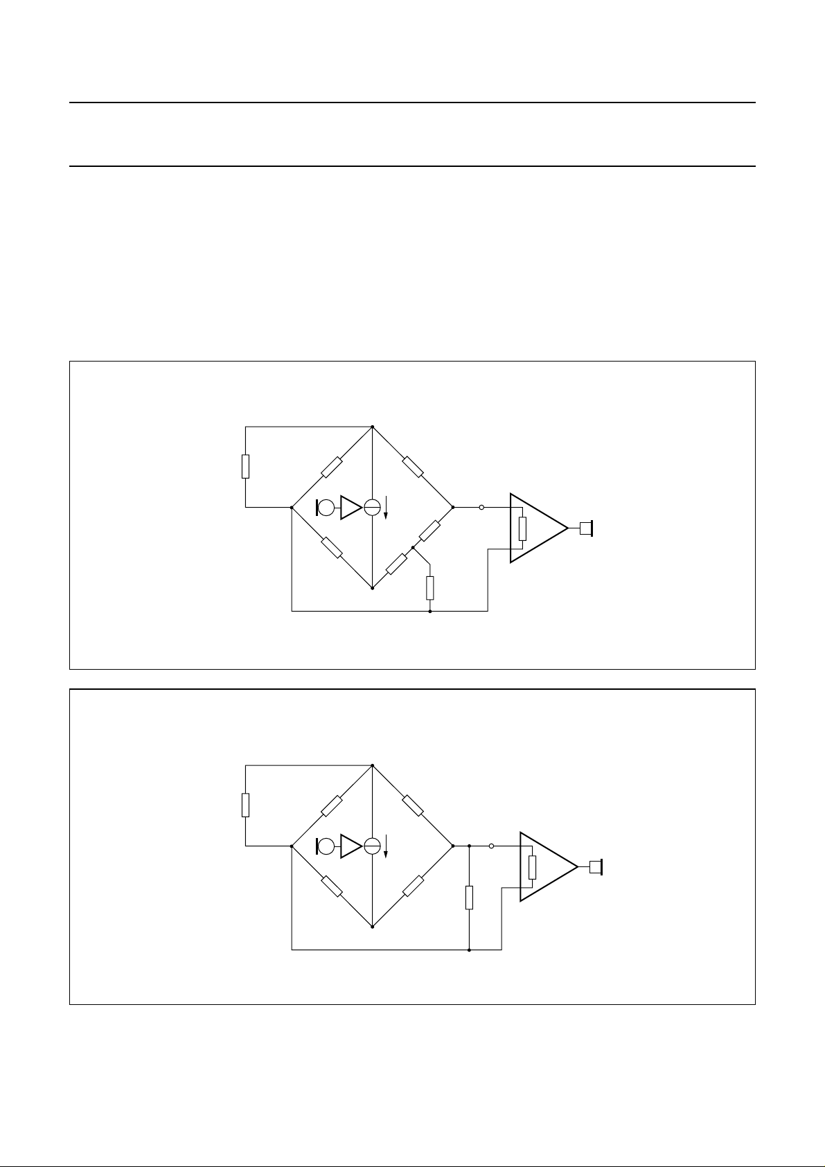
Fig.6 Equivalent circuit of an anti-sidetone network in a Wheatstone bridge configuration.
More information can be found in the designer guide; 9398 341 10011
IR
R
t
MSA501
June 1990 8
Philips Semiconductors Product specification
Low voltage versatile telephone
transmission circuit with dialler interface
RATINGS
Limiting values in accordance with the Absolute Maximum System (IEC 134)
PARAMETER CONDITIONS SYMBOL MIN. MAX. UNIT
Positive continuous line voltage V
Repetitive line voltage during
switch-on line interruption V
Repetitive peak line voltage for a
1 ms pulse per 5 s R9 = 20 Ω;
R10 = 13 Ω
(Fig.16) V
Line current TEA1067 (note 1) R9 = 20 Ω I
Line current TEA1067T (note 1) R9 = 20 Ω I
Voltage on all other pins V
Total power dissipation (note 2) R9 = 20 Ω
TEA1067 P
TEA1067T P
Storage temperature range T
Operating ambient temperature range T
Junction temperature T
line
line
−V
LN
LN
LN
i
i
tot
tot
stg
amb
j
TEA1067
− 12 V
− 13.2 V
− 28 V
− 140 mA
− 140 mA
− VCC+ 0.7 V
− 0.7 V
− 769 mW
− 550 mW
−40 + 125 °C
−25 + 75 °C
−+ 125 °C
Notes
1. Mostly dependent on the maximum required T
and on the voltage between LN and SLPE.
amb
See Figs 7 and 8 to determine the current as a function of the required voltage and the
temperature.
2. Calculated for the maximum ambient temperature specified T
= 75 °C and a maximum
amb
junction temperature of 125 °C.
THERMAL RESISTANCE
From junction to ambient in free air
TEA1067 R
TEA1067T mounted on glass epoxy board 41 × 19 × 1.5 mm R
th j-a
th j-a
typ. 65 K/W
typ. 90 K/W
June 1990 9
 Loading...