

Philips TEA1066T Datasheet
INTEGRATED CIRCUITS
DATA SH EET
TEA1066T
Versatile telephone transmission
circuit with dialler interface
Product specification
Supersedes data of September 1990
File under Integrated Circuits, IC03
1996 Apr 04
Philips Semiconductors Product specification
Versatile telephone transmission circuit
TEA1066T
with dialler interface
FEATURES
• Voltage regulator with adjustable static resistance
• Provides supply for external circuitry
• Symmetrical low-impedance inputs for dynamic and
magnetic microphones
• Symmetrical high-impedance inputs for piezoelectric
microphone
• Asymmetrical high-impedance input for electret
microphone
• Dual-tone multi-frequency (DTMF) signal input with
confidence tone
• Mute input for pulse or DTMF dialling
• Power down input for pulse dial or register recall
QUICK REFERENCE DATA
SYMBOL PARAMETER CONDITIONS MIN. TYP. MAX. UNIT
V
I
I
V
G
LN
line
CC
CC
v
line voltage I
line current normal operation 10 − 140 mA
internal supply current power down input LOW − 0.96 1.3 mA
supply voltage for peripherals I
voltage gain range for microphone amplifier
low impedance inputs (pins 7 and 9) 44 − 60 dB
high impedance inputs (pins 8 and 10) 30 − 46 dB
receiving amplifier 17 − 39 dB
T
amb
operating ambient temperature −25 − +75 °C
Line loss compensation
∆G
V
R
v
exch
exch
gain control 5.5 5.9 6.3 dB
exchange supply voltage 24 − 60 V
exchange feeding bridge resistance 400 − 1000 Ω
• Receiving amplifier for magnetic, dynamic or
piezoelectric earpieces
• Large gain setting range on microphone and earpiece
amplifiers
• Line loss compensation facility, line current dependent
(microphone and earpiece amplifiers)
• Gain control adaptable to exchange supply
• DC line voltage adjustment facility.
GENERAL DESCRIPTION
The TEA1066T is a bipolar integrated circuit that performs
all speech and line interface functions required in fully
electronic telephone sets. The circuit performs electronic
switching between dialling and speech.
= 15 mA 4.25 4.45 4.65 V
line
power down input HIGH − 55 82 µA
= 15 mA; MUTE
line
2.8 3.05 − V
input HIGH; Ip= 1.2 mA
I
= 15 mA; MUTE
line
2.5 − − V
input HIGH; Ip= 1.7 mA
ORDERING INFORMATION
TYPE
NUMBER
TEA1066T SO20
NAME DESCRIPTION VERSION
plastic small outline package; 20 leads; body width 7.5 mm SOT163-1
1996 Apr 04 2
PACKAGE
Philips Semiconductors Product specification
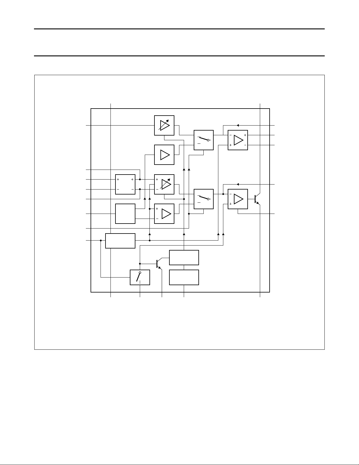
Fig.1 Block diagram.
The blocks marked ‘dB’ are attenuators.
handbook, full pagewidth
MEA009 - 1
dB
dB
SUPPLY AND
REFERENCE
AGC
CIRCUIT
SLPESTABAGCREGV
EE
CURRENT
REFERENCE
14
18 1912
16
15
7
8
10
9
13
17 1
6
5
4
11 20
IR
MICL+
MICH+
MICH−
MICL−
DTMF
MUTE
PD
V
CC
TEA1066T
LN
GAR
2
GAS1
3
GAS2
QR+
QR−
Versatile telephone transmission circuit
with dialler interface
BLOCK DIAGRAM
TEA1066T
1996 Apr 04 3
Philips Semiconductors Product specification
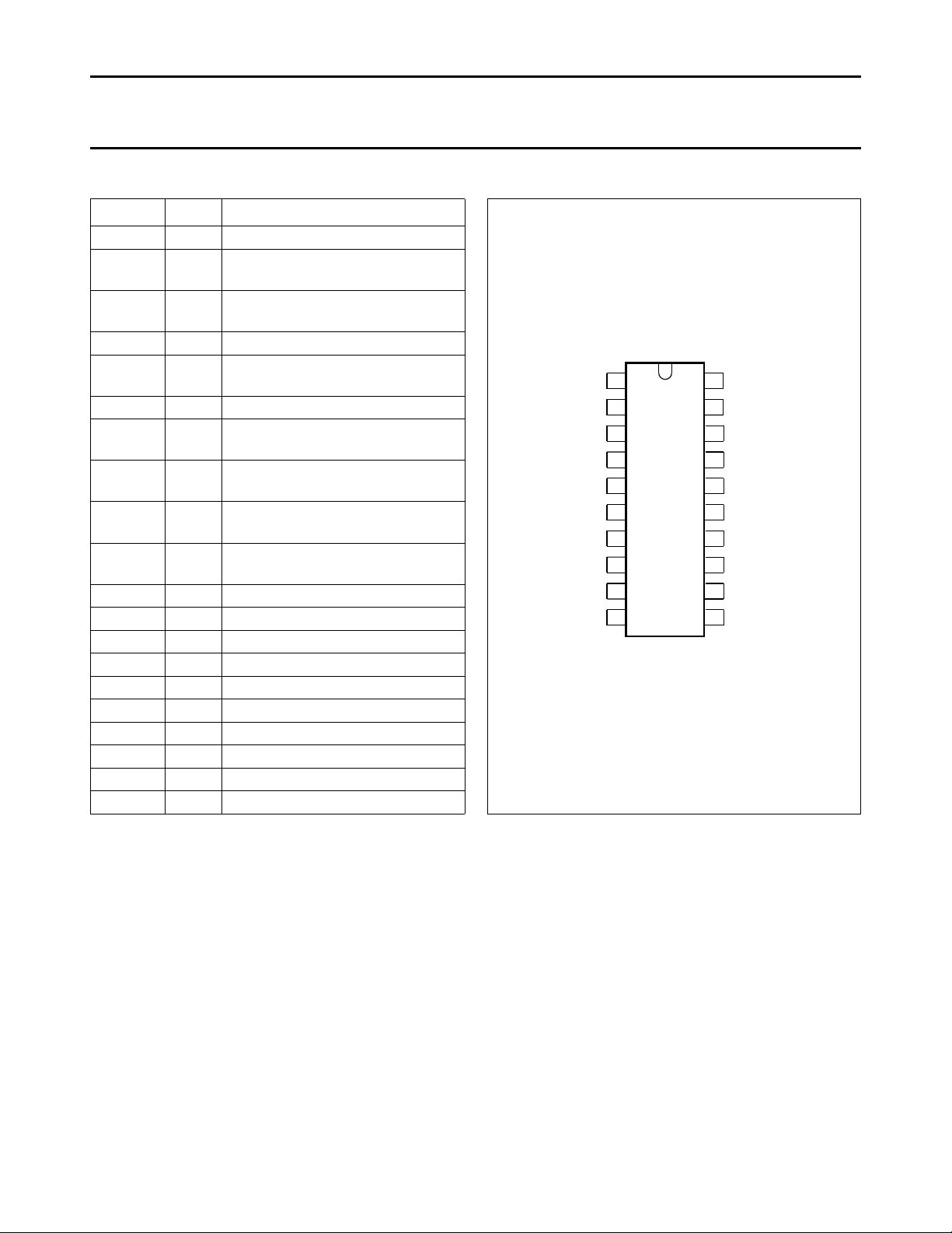
Fig.2 Pin configuration.
handbook, halfpage
1
2
3
4
5
6
7
8
9
10
20
19
18
17
16
15
14
13
12
11
MBH120
TEA1066T
LN
GAS1
GAS2
QR−
QR+
GAR
MICL−
MICH−
MICL+
SLPE
AGC
REG
V
CC
IR
DTMF
V
EE
MUTE
PD
STAB
MICH+
Versatile telephone transmission circuit
with dialler interface
PINNING
SYMBOL PIN DESCRIPTION
LN 1 positive line terminal
GAS1 2 gain adjustment transmitting
amplifier
GAS2 3 gain adjustment transmitting
amplifier
QR− 4 inverting output receiving amplifier
QR+ 5 non-inverting output receiving
amplifier
GAR 6 gain adjustment receiving amplifier
MICL− 7 inverting microphone input, low
impedance
MICH− 8 inverting microphone input, high
impedance
MICL+ 9 non-inverting microphone input, low
impedance
MICH+ 10 non-inverting microphone input,
high impedance
STAB 11 current stabilizer
V
EE
IR 13 receiving amplifier input
PD 14 power-down input
DTMF 15 dual-tone multi-frequency input
MUTE 16 mute input
V
CC
REG 18 voltage regulator decoupling
AGC 19 automatic gain control input
SLPE 20 slope (DC resistance) adjustment
FUNCTIONAL DESCRIPTION
Supplies: VCC, LN, SLPE, REG and STAB
Power for the TEA1066T and its peripheral circuits is
usually obtained from the telephone line. The TEA1066T
develops its own supply voltage at V
voltage drop. The supply voltage VCC may also be used to
supply external peripheral circuits, e.g. dialling and control
circuits.
The supply has to be decoupled by connecting a
smoothing capacitor between VCC and VEE; the internal
voltage regulator has to be decoupled by a capacitor from
REG to VEE. An internal current stabilizer is set by a
resistor of 3.6 kΩ between STAB and VEE.
12 negative line terminal
17 supply voltage decoupling
and regulates its
CC
TEA1066T
The DC current flowing into the set is determined by the
exchange supply voltage (V
resistance (R
(R
) and the DC voltage on the subscriber set
line
), the DC resistance of the telephone line
exch
(see Fig.7).
If the line current I
exceeds the current ICC+ 0.5 mA
line
required by the circuit itself (approximately 1 mA) plus the
current Ip required by the peripheral circuits connected to
VCC, then the voltage regulator diverts the excess current
via LN.
), the feeding bridge
exch
1996 Apr 04 4
Philips Semiconductors Product specification
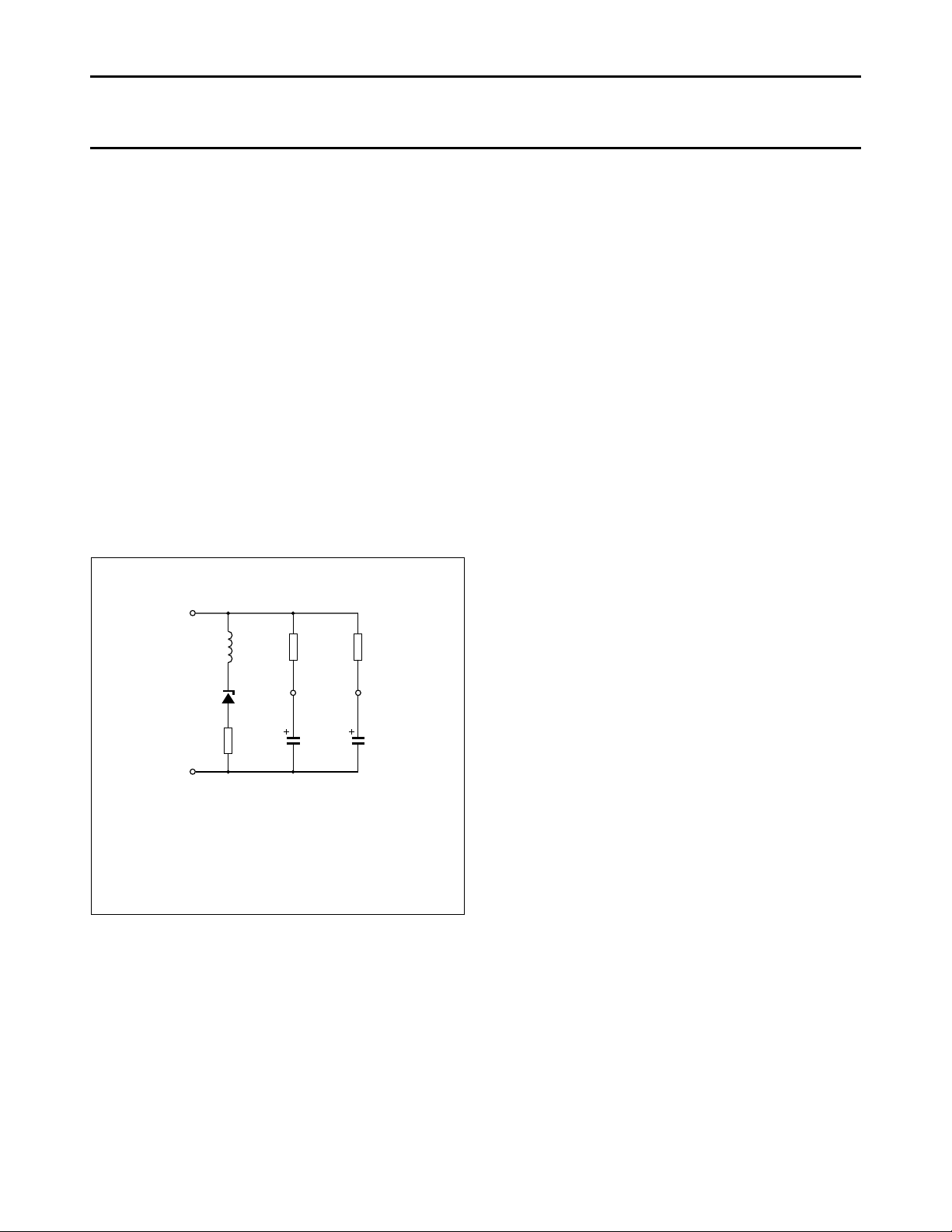
Fig.3 Equivalent impedance circuit.
Rp= 17.5kΩ
Leq= C3× R9 × R
p
handbook, halfpage
REG
V
EE
V
CC
LN
MBA454
L
eq
R
p
R1
V
ref
R9
20 Ω
C3
4.7 µF C1100 µF
Versatile telephone transmission circuit
with dialler interface
The voltage regulator adjusts the average voltage on
LN to:
VLN= V
or
VLN= V
where V
compensated reference voltage of 4.2 V and R9 is an
external resistor connected between SLPE and VEE.
The preferred value for R9 is 20 Ω. Changing the value of
R9 will also affect microphone gain, DTMF gain, gain
control characteristics, side-tone level and the maximum
output swing on LN.
Under normal conditions, when I
the static behaviour of the circuit is that of a 4.2 V regulator
diode with an internal resistance equal to that of R9. In the
audio frequency range, the dynamic impedance is largely
determined by R1 (see Fig.3).
+ I
ref
+ (I
ref
is an internally generated temperature
ref
× R9
SLPE
− ICC− 0.5 × 10⁻³A − Ip) × R9
line
>> ICC+ 0.5 mA + Ip,
SLPE
TEA1066T
and > 3 V, this being the minimum supply voltage for most
CMOS circuits, including voltage drop for an enable diode.
If MUTE is LOW, the available current is further reduced
when the receiving amplifier is driven.
Microphone inputs MICL+, MICH+, MICL− and MICH−
and amplification adjustment connections GAS1 and
GAS2
The TEA1066T has symmetrical microphone inputs.
The MICL+ and MICL− inputs are intended for
low-sensitivity, low-impedance dynamic or magnetic
microphones. The input impedance is 8.2 kΩ (2 × 4.1 kΩ)
and its voltage gain is typically 52 dB. The MICH+ and
MICH− inputs are intended for a piezoelectric microphone
or an electret microphone with a built-in FET source
follower. Its input impedance is 40.8 kΩ (2 × 20.4 kΩ) and
its voltage gain is typical 38 dB.
The arrangements with the microphone types mentioned
are shown in Fig.9.
The internal reference voltage can be adjusted by means
of an external resistor RVA. This resistor, connected
between LN and REG (pins 1 and 18), will decrease the
internal reference voltage; when connected between REG
and SLPE (pins 18 and 20) it will increase the internal
reference voltage.
Current Ip, available from VCC for supplying peripheral
circuits, depends on external components and on the line
current. Figure 8 shows this current for VCC> 2.2 V
The gain of the microphone amplifier in both types can be
adjusted over a range of ±8 dB to suit the sensitivity of the
transducer used. The gain is proportional to external
resistor R7 connected between GAS1 and GAS2.
An external capacitor C6 of 100 pF between GAS1 and
SLPE is required to ensure stability. A larger value may be
chosen to obtain a first-order low-pass filter. The cut-off
frequency corresponds with the time constant R7 × C6.
Mute input MUTE
A HIGH level at MUTE enables the DTMF input and
inhibits the microphone inputs and the receiving amplifier;
a LOW level or an open circuit has the reverse effect.
Switching the mute input will cause negligible clicks at the
earpiece outputs and on the line.
Dual-tone multi frequency input DTMF
When the DTMF input is enabled, dialling tones may be
sent onto the line. The voltage gain from DTMF to LN is
typically 25.5 dB and varies with R7 in the same way as
the gain of the microphone amplifier. The signalling tones
can be heard in the earpiece at a low level (confidence
tone).
Receiving amplifier: IR, QR+, QR− and GAR
The receiving amplifier has one input IR and two
complementary outputs, a non-inverting output QR+ and
an inverting output QR−.
1996 Apr 04 5

Philips Semiconductors Product specification
× R1 R3 R8//Z
bal
[ ]+( )=
( )⁄ Z
lineZline
R1+( )⁄=
Versatile telephone transmission circuit
with dialler interface
These outputs may be used for single-ended or for
differential drive, depending on the sensitivity and type of
earpiece used (see Fig.10). Gain from IR to QR+ is
typically 25 dB. This will be sufficient for low-impedance
magnetic or dynamic earpieces, which are suited for
single-ended drive. By using both outputs (differential
drive), the gain is increased by 6 dB and differential drive
becomes possible. This feature can be used when the
earpiece impedance exceeds 450 Ω (high-impedance
dynamic, magnetic or piezoelectric earpieces).
The output voltage of the receiving amplifier is specified for
continuous-wave drive. The maximum output voltage will
be higher under speech conditions, where the ratio of peak
to RMS value is higher.
The receiving amplifier gain can be adjusted over a range
of ±8 dB to suit the sensitivity of the transducer used.
The gain is set by the external resistor R4 connected
between GAR and QR+.
Two external capacitors, C4 = 100 pF and
C7 = 10 × C4 = 1 nF, are necessary to ensure stability.
A larger value of C4 may be chosen to obtain a first-order,
low-pass filter. The ‘cut-off’ frequency corresponds with
the time constant R4 × C4.
Automatic gain control input AGC
Automatic line loss compensation is obtained by
connecting a resistor R6 between AGC and VEE. This
automatic gain control varies the microphone amplifier
gain and the receiving amplifier gain in accordance with
the DC line current.
The control range is 6 dB. This corresponds with a line
length of 5 km for a 0.5 mm diameter copper twisted-pair
cable with a DC resistance of 176 Ω/km and an average
attenuation of 1.2 dB/km.
Resistor R6 should be chosen in accordance with the
exchange supply voltage and its feeding bridge resistance
(see Fig.11 and Table 1). Different values of R6 give the
same ratio of line currents for start and end of the control
range.
If automatic line loss compensation is not required, AGC
may be left open. The amplifiers then all give their
maximum gain as specified.
Power-down input PD
During pulse dialling or register recall (timed loop break)
the telephone line is interrupted, as a consequence it
provides no supply for the transmission circuit and the
peripherals connected to VCC. These gaps have to be
TEA1066T
bridged by the charge in the smoothing capacitor C1.
The requirements on this capacitor are relaxed by applying
a HIGH level to the PD input during the time of the loop
break, which reduces the supply current from typically
1 mA to typically 55 µA.
A HIGH level at PD further disconnects the capacitor at
REG, with the effect that the voltage stabilizer will have no
switch-on delay after line interruptions. This results in no
contribution of the IC to the current waveform during pulse
dialling or register recall. When this facility is not required
PD may be left open.
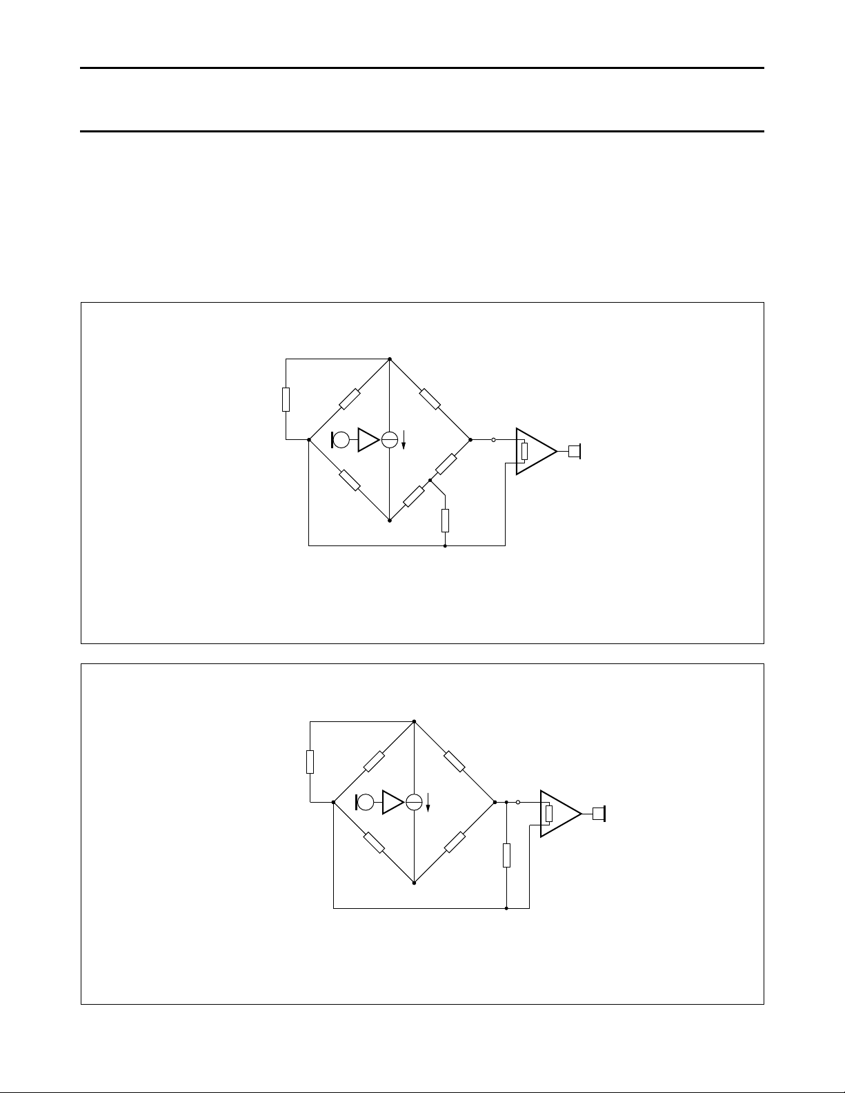
Side-tone suppression
Suppression of the transmitted signal in the earpiece is
obtained by the anti-side-tone network consisting of
R1//Z
compensation is obtained when the following conditions
are fulfilled:
R9 R2
Z
If fixed values are chosen for R1, R2, R3, and R9, then
condition (1) will always be fulfilled, provided that
R8//Z
suppression, condition (2) has to be fulfilled, resulting in:
Z
k = (R8/R1).
Scale factor k (dependent on the value of R8) must be
chosen to meet the following criteria:
1. Compatibility with a standard capacitor from the E6 or
2. Z
3. Z
In practice, Z
type; consequently, an average value has to be chosen for
Z
with which Z
Example: The balanced line impedance Z
the optimum suppression is preset can be calculated by:
Assume Z
5 km line of 0.5 mm diameter, copper, twisted-pair cable
matched to 600 Ω (176 Ω/km; 38 nF/km). When k = 0.64,
then R8 = 390 Ω; Z
The anti-side-tone network for the TEA1060 family shown
in Fig.4 attenuates the signal received from the line by
32 dB before it enters the receiving amplifier.
, R2, R3, R8, R9 and Z
line
balZbal
= (R8/R1) Z
bal
E12 range for Z
. The suppression further depends on the accuracy
bal
R8+
< R3. To obtain optimum side-tone
bal
= k × Z
line
bal
//R8 << R3
bal
+ R8 >> R9.
bal
varies greatly with line length and cable
line
/k equals the average line impedance.
bal
= 210 Ω + (1265 Ω/140 nF), representing a
line
= 130 Ω + (820 Ω//220 nF).
bal
(see Fig.14). Maximum
bal
, where k is a scale factor:
line
at which
bal
(1)
(2)
1996 Apr 04 6
Philips Semiconductors Product specification
Fig.4 Equivalent circuit of TEA1060 family anti-side-tone bridge.
handbook, full pagewidth
MSA500 - 1
IR
R3
R8
SLPE
R9
Z
line
V
EE
Z
bal
i
m
R
t
R1 R2
LN
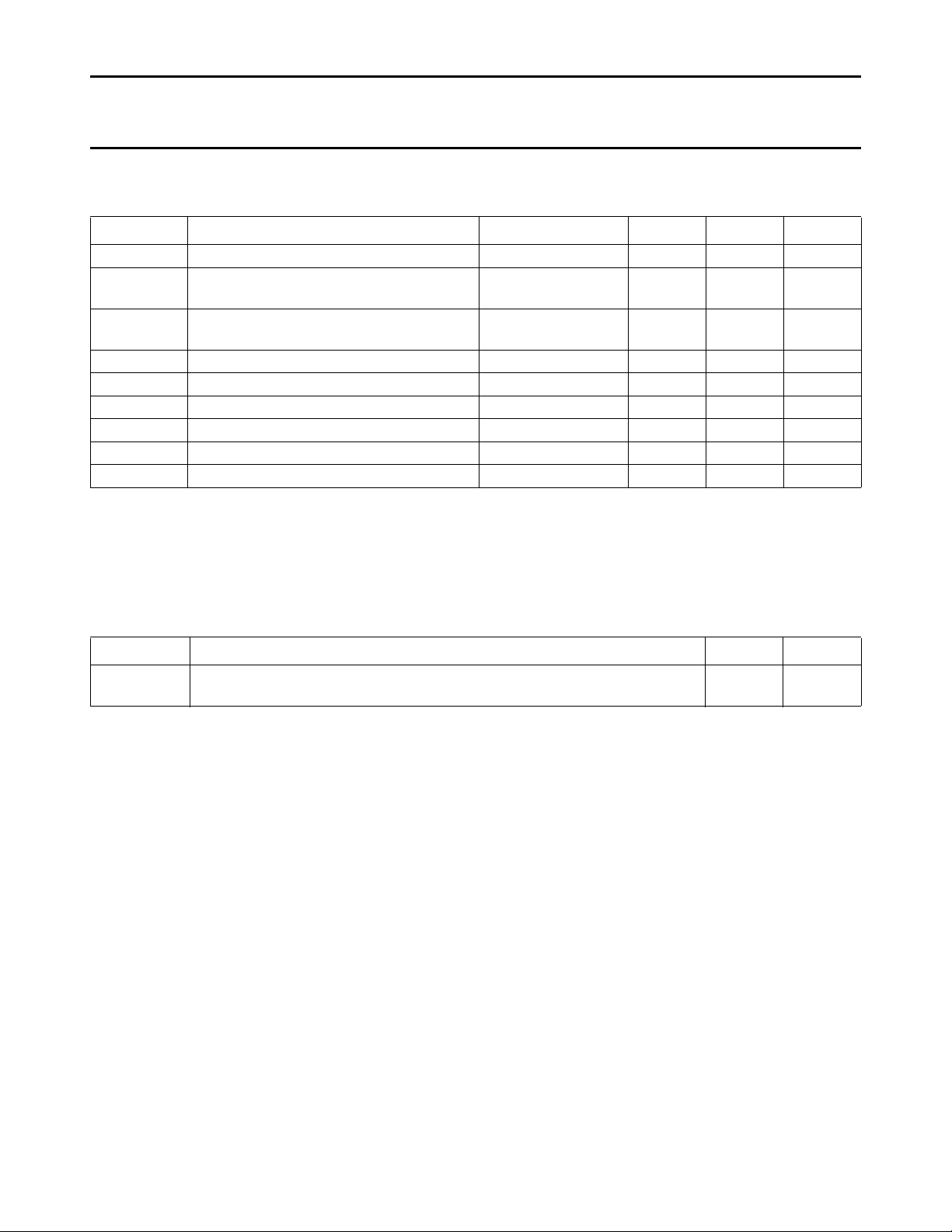
Fig.5 Equivalent circuit of an anti-side-tone network in a Wheatstone bridge configuration.
handbook, full pagewidth
MSA501 - 1
IR
R8
SLPE
R9
R1
LN
Z
line
V
EE
Z
bal
R
A
i
m
R
t
Versatile telephone transmission circuit
with dialler interface
The attenuation is almost constant over the whole audio
frequency range. Figure 5 shows a conventional
Wheatstone bridge anti-side-tone circuit that can be used
as an alternative. Both bridge types can be used with
either resistive or complex set impedances.
The anti-side-tone network as used in the standard
application (see Fig.13) attenuates the signal from the line
TEA1066T
with 32 dB. The attenuation is nearly flat over the
audio-frequency range.
Instead of the previously-described special TEA1066
bridge, the conventional Wheatstone bridge configuration
can be used as an alternative anti-side-tone circuit. Both
bridge types can be used with either a resistive set
impedance or a complex set impedance.
1996 Apr 04 7
Philips Semiconductors Product specification
Versatile telephone transmission circuit
TEA1066T
with dialler interface
LIMITING VALUES
In accordance with the Absolute Maximum Rating System (IEC 134).
SYMBOL PARAMETER CONDITIONS MIN. MAX. UNIT
V
LN
V
LN(R)
V
LN(RM)
I
line
V
n
P
tot
T
stg
T
amb
T
j
Notes
1. Mostly dependent on the maximum required T
2. Calculated for the maximum ambient temperature specified, T
125 °C.
positive continuous line voltage − 12 V
repetitive line voltage during switch-on or
− 13.2 V
line interruption
repetitive peak line voltage for a 1 ms pulse
per 5 s
R9 = 20 Ω;
R10 = 13 Ω; (Fig.10)
− 28 V
line current R9= 20 Ω; note 1 − 140 mA
voltage on any other pin VEE− 0.7 VCC+ 0.7 V
total power dissipation R9= 20 Ω; note 2 − 555 mW
IC storage temperature −40 +125 °C
operating ambient temperature −25 +75 °C
junction temperature − 125 °C
and on the voltage between LN and SLPE (see Fig.6).
amb
= 75 °C and a maximum junction temperature of
amb
THERMAL CHARACTERISTICS
SYMBOL PARAMETER VALUE UNIT
R
th j-a
thermal resistance from junction to ambient in free air mounted on glass epoxy
90 K/W
board 41 × 19 × 1.5 mm
1996 Apr 04 8
 Loading...