


INTEGRATED CIRCUITS
DATA SH EET
TEA1065
Versatile telephone transmission
circuit with dialler interface
Product specification
File under Integrated Circuits, IC03A
March 1994
Philips Semiconductors Product specification
Versatile telephone transmission circuit with
dialler interface
FEATURES
• Current and voltage regulator mode with adjustable
static resistances
• Provides supply for external circuitry
• Symmetrical high-impedance inputs for piezoelectric
microphone
• Asymmetrical high-impedance input for electret
microphone
• DTMF signal input with confidence tone
• Mute input for pulse or DTMF dialling
• Power-down input for pulse dial or register recall
• Digital pulse input to drive an external switch transistor
• Receiving amplifier for magnetic, dynamic or
piezoelectric earpieces
ORDERING INFORMATION
EXTENDED TYPE
NUMBER
PINS PIN POSITION MATERIAL CODE
TEA1065 24 DIL plastic SOT101L
TEA1065T 24 SO24 plastic SOT137A
• Large gain setting range on microphone and earpiece
amplifiers
• Line loss compensation facility, line current dependent
(on microphone and earpiece amplifiers)
• Adjustable gain control
• DC line voltage adjustment facility
GENERAL DESCRIPTION
The TEA1065 is a bipolar integrated circuit which performs
all speech and line interface functions that are required in
fully electronic telephone sets with adjustable DC mask.
The circuit performs electronic switching between dialling
and speech internally.
PACKAGE
TEA1065
Notes
1. SOT101-1; 1998 Jun 18.
2. SOT137-1; 1998 Jun 18.
QUICK REFERENCE DATA
SYMBOL PARAMETER CONDITIONS MIN. TYP. MAX. UNIT
V
I
I
LN
line
CC
line voltage I
= 15 mA 4.25 4.45 4.65 V
line
normal operation line current range 10 − 150 mA
internal supply consumption
power-down input LOW − 1.14 1.5 mA
power-down input HIGH − 73 105 µA
V
CC
supply voltage for peripherals I
= 15 mA;
line
MUTE input
HIGH
IP= 1.2 mA 2.7 −−V
= 1.55 mA 2.5 −−V
I
P
G
V
voltage gain range
microphone amplifier 30 − 46 dB
earpiece amplifier 20 − 45 dB
∆G
V
line loss compensation
gain control range −5.5 −5.9 −6.3 dB
T
amb
operating ambient temperature range −25 −+75 °C
March 1994 2
Philips Semiconductors Product specification
Versatile telephone transmission circuit with
dialler interface
handbook, full pagewidth
DTMF
MUTE
MIC+
MIC−
V
CC
PD
17
IR
+
−
TEA1065
8
7
19
dB
+
−
−
+
20
21
SUPPLY AND
18
REFERENCE
CONTROL
CURRENT
CURRENT
REFERENCE
TEA1065
6
GAR
−
+
−
+
−
+
BANDGAP
REFERENCE
+
−
LINE
CURRENT
CONTROL
5
QR+
4
QR−
2
GAS1
1
LN
24
SLPE
3
GAS2
11
VBG
13
REFI
12
DOC
2216
23 9 15
V
EE
REG AGC STAB
Fig.1 Block diagram.
March 1994 3
DPI
14
10
VSI
CURL
MBA557
Philips Semiconductors Product specification
V ersatile telephone transmission circuit with
dialler interface
PINNING
SYMBOL PIN DESCRIPTION
LN 1 positive line terminal
GAS1 2 gain adjustment; sending amplifier
GAS2 3 gain adjustment; sending amplifier
QR− 4 inverting output; receiving amplifier
QR+ 5 non-inverting output; receiving
amplifier
GAR 6 gain adjustment; receiving amplifier
MIC− 7 inverting microphone input
MIC+ 8 non-inverting microphone input
STAB 9 current stabilizer
DPI 10 digital pulse input
VBG 11 bandgap output reference
DOC 12 drive current output
REFI 13 reference voltage input
VSI 14 voltage sense input
CURL 15 current limitation input
V
EE
IR 17 receiving amplifier input
PD 18 power-down input
DTMF 19 dual-tone multifrequency input
MUTE 20 MUTE input
V
CC
REG 22 voltage regulator decoupling
AGC 23 automatic gain control input
SLPE 24 slope (DC resistance) adjustment
16 negative line terminal
21 positive supply decoupling
handbook, halfpage
1
LN
GAS1
2
3
GAS2
4
QR−
QR+
5
6
GAR
MIC−
MIC+
STAB
DPI
VBG
DOC
7
8
9
10
11
12
TEA1065
MBA551
Fig.2 Pinning diagram.
TEA1065
SLPE
24
23
AGC
22
REG
V
21
CC
20
MUTE
19
DTMF
18
PD
17
IR
V
16
EE
CURL
15
VSI
14
REFI
13
March 1994 4
Philips Semiconductors Product specification
V ersatile telephone transmission circuit with
dialler interface
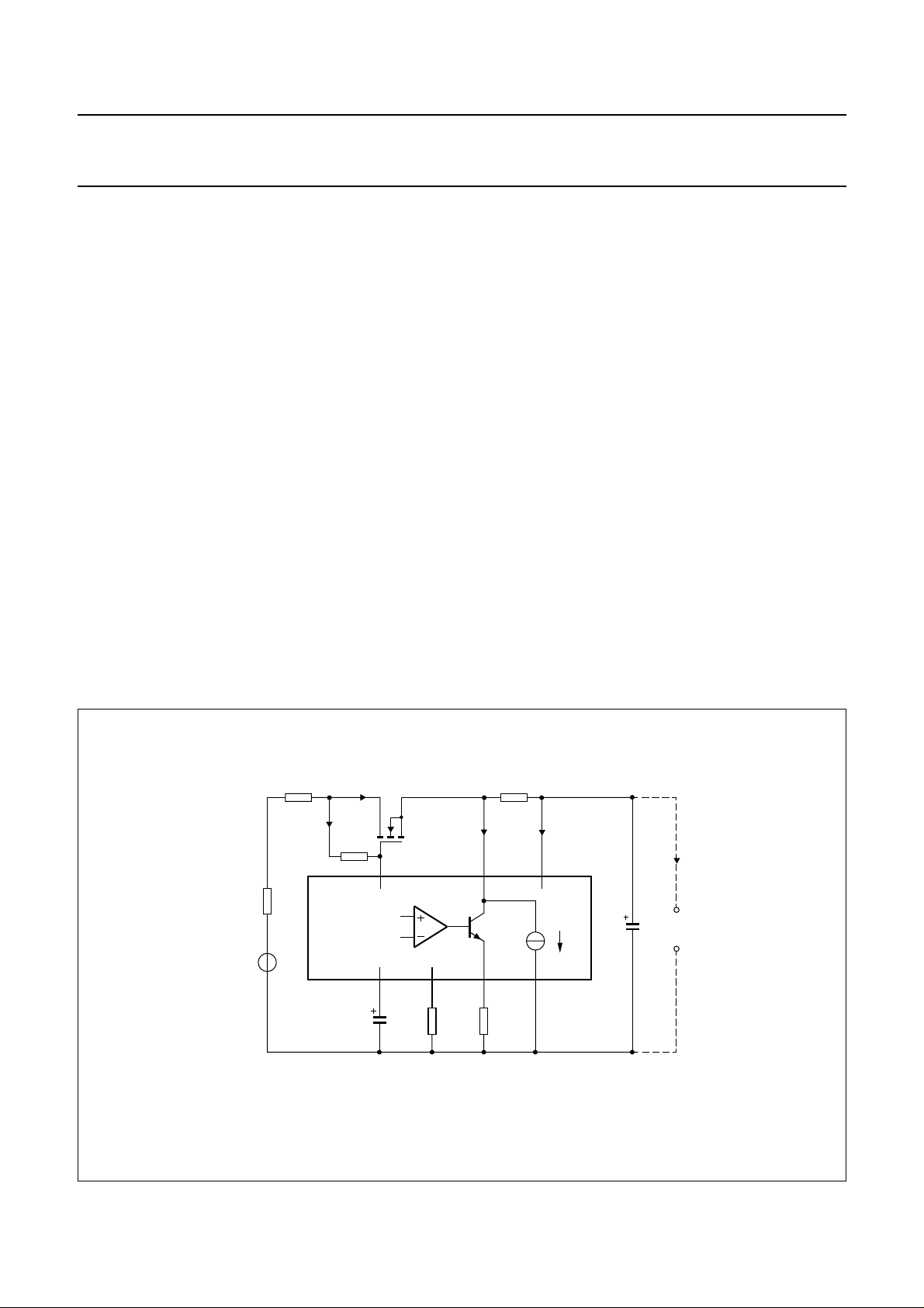
FUNCTIONAL DESCRIPTION
Supply: V
The circuit and its peripherals are usually supplied from the
telephone line. The circuit develops its own supply voltage
at V
CC
and SLPE (pins 1 and 24). The internal supply requires a
decoupling capacitor between VCCand VEE(pin 16); the
internal voltage regulator has to be decoupled by a
capacitor from REG (pin 22) to VEE. The internal current
stabilizer is set by a 3.6 kΩ resistor connected between
STAB (pin 9) and VEE.
The TEA1065 can be set either in a DC voltage regulator
mode or in a DC current regulator mode. The DC mask can
be selected by connecting the appropriate external
components to the dedicated pins (VSI, REFI, DOC,
VBG).
When the DC current regulator mode is not required it can
be cancelled by connecting pin VSI to VEE; pins REFI,
VBG and DOC are left open-circuit.
Voltage regulator mode
The voltage regulator mode is achieved when the line
current is less than the current I
With R13 = R14 = 30 kΩ, the current I
(Ip= 0 mA).
, LN, SLPE, REG and STAB
CC
(pin 21) and regulates its voltage drop between LN
as illustrated in Fig.3.
knee
= 30 mA
knee
TEA1065
This line current value will be reached when the voltage on
pin VSI (almost equal to the voltage on pin SLPE) exceeds
the voltage on pin REFI (equal to the voltage on pin VBG
divided by the resistor tap R13, R14). For other values of
R13 and R14, the I
formula:
I
knee=ICC
+ IP+ (VBG/R9) × {R14/(R14 + R13)}
− (R15/R9) × IO(VSI)
ICCis the current required by the circuit itself
(typ. 1.14 mA). IPis the current required by the peripheral
circuits connected between VCCand VEE. I
output current from pin VSI (typ. 2.5 µA).
The DC slope of the V
determined by R9 (R9 = R9a + R9b) in series with the
rdsof the external line current control transistor (see Fig.4;
rds= ∂VGS/∂IDat VGS=VDS).
Current regulator mode
The current regulator mode is achieved when the line
current is greater than I
V
curve is approximately 1300 Ω with R9 = 20 Ω,
line/Iline
R16 = 1 MΩ, R13 = R14 = 30 kΩ. For other values of
these resistances, the slope value can be approximated by
the following formula:
R9 × {1 + R16 × (1/R13 + 1/R14)}
current is given by the following
knee
O(VSI)
curve is, in this mode,
line/Iline
. In this mode, the slope of the
knee
is the
handbook, full pagewidth
line
current
I
knee
0
0
voltage
regulator
mode
current
regulator
mode
Fig.3 Voltage and current regulator mode.
March 1994 5
MBA567
set
voltage
Philips Semiconductors Product specification
V ersatile telephone transmission circuit with
dialler interface
The DC current flowing into the set is determined by the
exchange supply voltage (V
subscriber line (R
) and the DC voltage on the subscriber
line
set (see Fig.4).
If the line current exceeds ICC+ 0.3 mA, required by the
circuit itself (ICC≈ 1.14 mA), plus the current Iprequired by
the peripheral circuits connected to VCCthen the voltage
regulator will divert the excess current via LN.
VLN=V
where: V
ref
+ I
V
ref
× R9 =
SLPE
+ (I
ref
− ICC− 0.3 × 10⁻³− Ip) × R9
line
is an internally generated temperature
compensated reference voltage of 4.18 V and R9 is an
external resistor connected between SLPE and VEE.
The preferred value of R9 is 20 Ω. Changing R9 will
influence the microphone gain, gain control
characteristics, sidetone and the maximum output swing
on LN. In this instance, the voltage on the line (excluding
the diode rectifier bridge; see Fig.4) is:
V
line=VLN
+ VGS+ R16 × I
where: VGSis the voltage drop between the gate and
source terminal of the external line current control
transistor and I
(I
= 0 in the voltage regulator mode and increases with
DOC
is the current sunk by pin DOC
DOC
), the DC resistance of the
exch
DOC
TEA1065
I
in the current regulator mode).
line
Under normal conditions I
for the voltage regulator mode (I
behaviour of the circuit is equal to a 4.18 V voltage
regulator diode with an internal resistance of R9 in series
with the V
of the external line current control
GSon
transistor. For the current regulator mode (I
static behaviour of the circuit is equal to a 4.18 V voltage
regulator diode with an internal resistance of R9 in series
with the V
of the external line current control transistor
GSon
and also in series with a DC voltage source R16
× I
(the preferred value of R16 is 1 MΩ at this value the
DOC
current I
is negligible compared to I
DOC
In the audio frequency range the dynamic impedance
between LN and VEEis equal to R1 (see Fig.8). The
internal reference voltage V
of an external resistor RVA. This resistor, connected
between LN and REG, will decrease the internal reference
voltage. When RVAis connected between REG and SLPE
the internal reference voltage will increase.
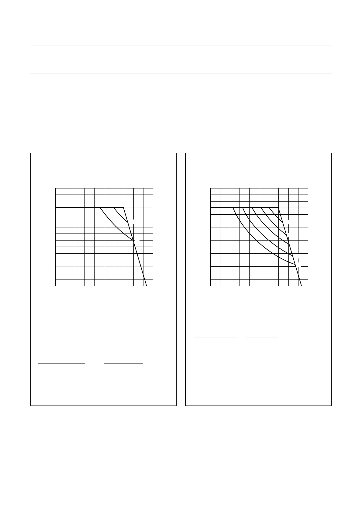
The maximum allowed line current is given in Figs 5 and 6,
where the current is shown as a function of the required
reference voltage, ambient temperature and applied
package.
>> ICC+ 0.3 mA + Ipand
SLPE
< I
line
can be adjusted by means
ref
), the static
knee
line
).
line
> I
knee
), the
handbook, full pagewidth
V
R
exch
exch
R
line
I
DOC
V
line
I
R16
TEA1065
line
I
SLPE
+ 0.5 mA
DC
AC
22 9
REG V
C3 R5 R9
STAB
Fig.4 Supply arrangement.
March 1994 6
LNDOC
12112
24
SLPE
R1
I
CC
V
CC
0.3 mA
16
EE
C1
peripheral
circuits
MBA550
I
p
Philips Semiconductors Product specification
V ersatile telephone transmission circuit with
dialler interface
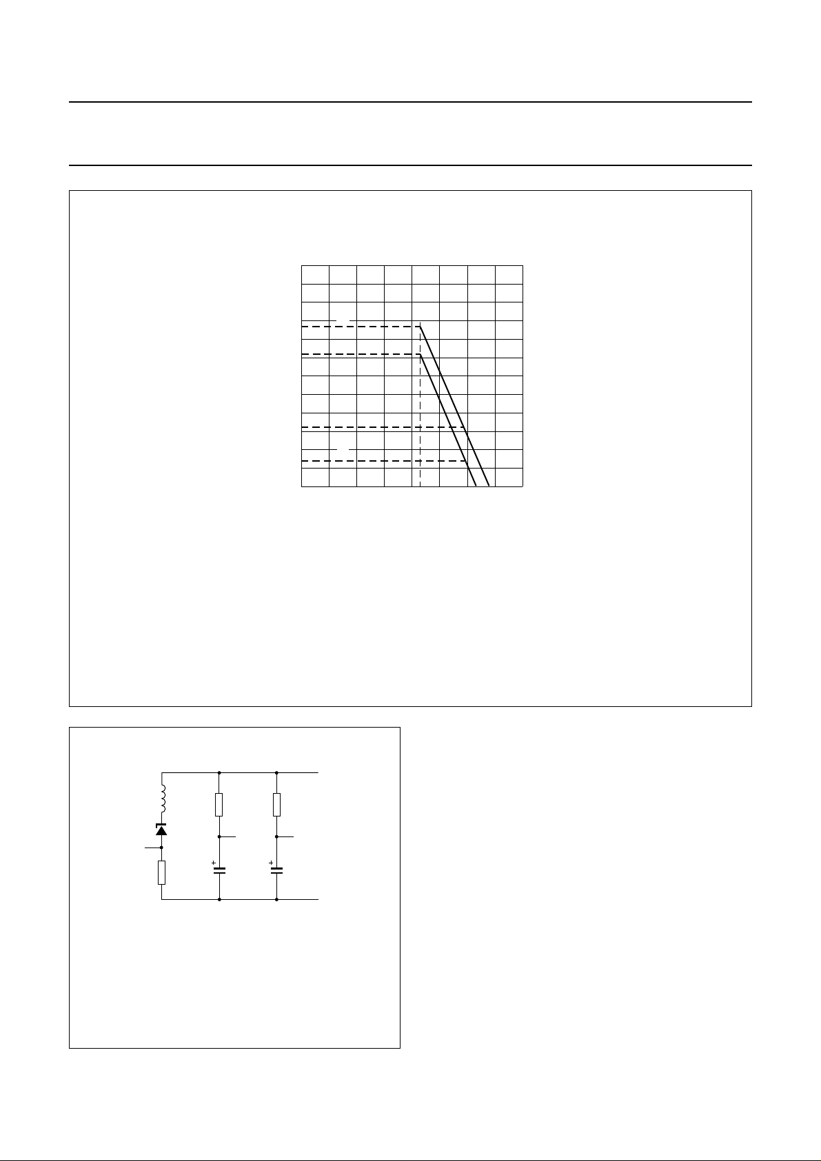
The current Ip, available from VCCfor supplying peripheral
circuits, depends on the external components and on the
line current. Fig.7 shows this current for VCC> 2.2 V and
for VCC> 3 V, where 3 V is the minimum supply voltage for
most CMOS circuits including a diode voltage drop for a
back-up diode. If MUTE is LOW the available current is
further reduced when the receiving amplifier is driven
(earpiece amplifier supplied from VCC).
handbook, halfpage
170
I
LN
(mA)
150
130
MBA570
(1)
handbook, halfpage
170
I
LN
(mA)
150
130
TEA1065
MBA571
(1)
110
(2)
90
70
50
30
212
46810
VLN-V
SLPE
(V)
110
90
70
50
30
212
T
amb
(1) 35 °C
(2) 45 °C
T
amb
(1) 65 °C
(2) 75 °C
Fig.5 TEA1065 safe operating area.
P
tot
1.2 W
1.0 W
(3) 55 °C
(4) 65 °C
(5) 75 °C
Fig.6 TEA1065T safe operating area.
(2)
(3)
(4)
(5)
46810
V
LN-VSLPE
P
tot
(V)
1.2 W
1.07 W
0.93 W
0.8 W
0.67 W
March 1994 7
Philips Semiconductors Product specification
V ersatile telephone transmission circuit with
dialler interface
handbook, halfpage
3
I
P
(mA)
2
1
0
(1)
(2)
(3)
(4)
012 4
3
VCC (V)
TEA1065
MBA569
I
= 15 mA at VLN= 4.45 V
line
R1 = 620 Ω
R9 = 20 Ω
Curve (1) and (3) are valid when the receiving amplifier is not driven or when MUTE =HIGH, curves (2) and (4)
are valid when MUTE = LOW and the receiving amplifier is driven, V
(1) = 2.2 mA; (2) = 1.77 mA; (3) = 0.78 mA and (4) = 0.36 mA.
= 150 mV, RL= 150 Ω (asymmetrical).
o(rms)
Fig.7 Maximum current Ipavailable from VCCfor external (peripheral) circuitry with VCC> 2.2 V and VCC> 3 V.
R1
V
C1
MBA552
CC
LN
V
EE
andbook, halfpage
SLPE
Leq=C3×R9 × R
Rp= 17.5 kΩ
L
eq
V
R9
20 Ω
p
ref
R
p
REG
C3
4.7 µF
Fig.8 Equivalent circuit impedance between LN
and VEE.
March 1994 8
Philips Semiconductors Product specification
V ersatile telephone transmission circuit with
dialler interface
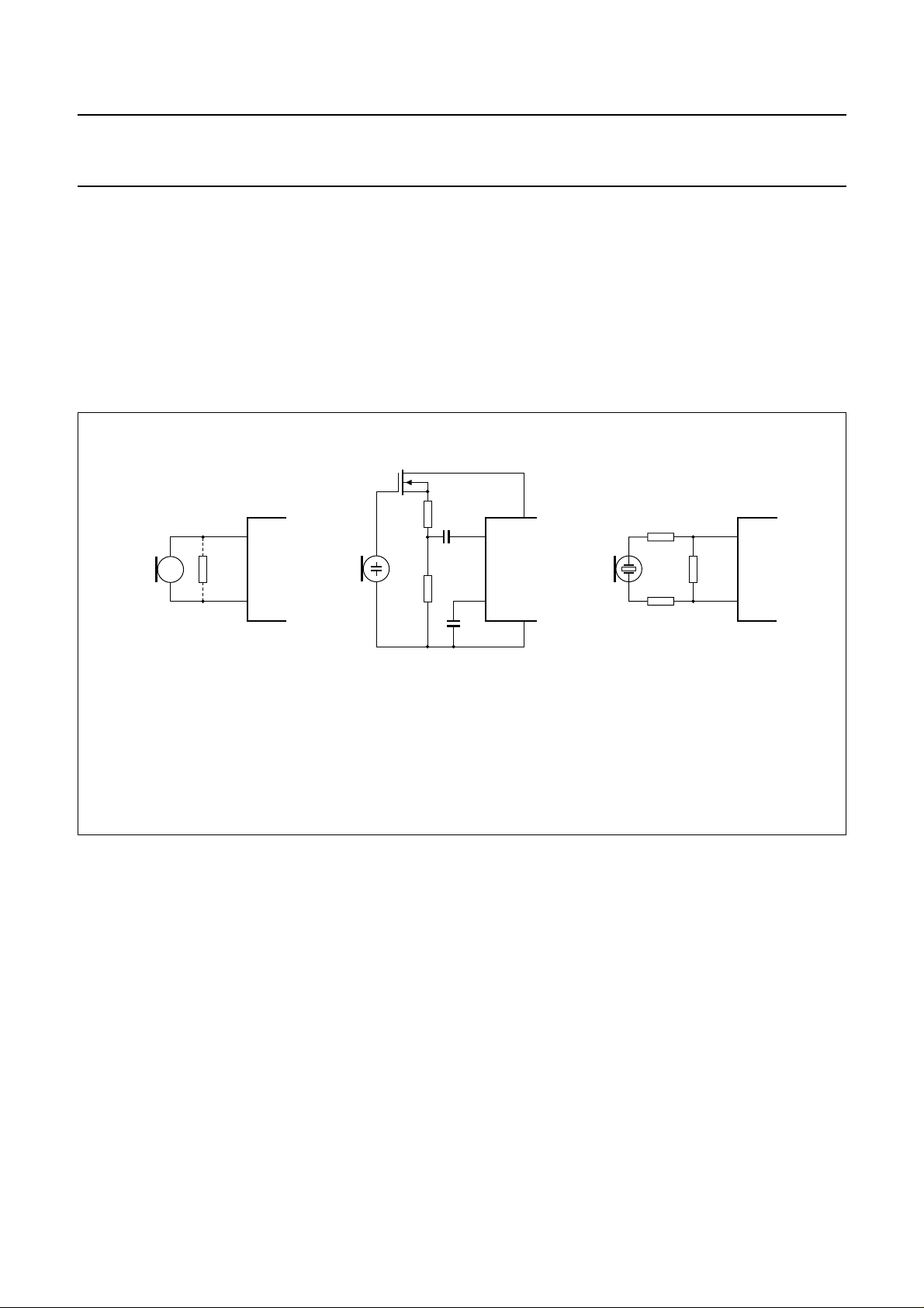
Microphone inputs MIC+ and MIC− and gain
adjustment connections GAS1 and GAS2
The TEA1065 has symmetrical microphone inputs, its
input impedance is 40.8 kΩ (2 × 20.4 kΩ) and its voltage
gain is typ. 38 dB with R7 = 68 kΩ. Either dynamic,
magnetic or piezoelectric microphones can be used, or an
electret microphone with a built-in FET buffer.
Arrangements for the microphones types are illustrated in
Fig.9.
handbook, full pagewidth
MIC+
(1)
MIC−
8
7
MIC−
MIC+
TEA1065
The gain of the microphone amplifier is proportional to
external resistor R7, connected between GAS1 and
GAS2, which can be adjusted between 30 dB and 46 dB to
suit the sensitivity of the transducer.
An external 100 pF capacitor (C6) is required between
GAS1 and SLPE to ensure stability. A larger value of C6
may be chosen to obtain a first-order low-pass filter. The
“cut-off” frequency corresponds with the time constant
R7 × C6.
V
CC
21
7
8
16
V
EE
MIC+
MIC−
8
7
MBA553
(a) (b)
(a) magnetic or dynamic microphone,
the resistor (1) may be connected to
reduce the terminating impedance, or
for sensitive types a resistive
attenuator can be used to prevent
overloading the microphone inputs;
(c)
(b) electret microphone; (c) piezoelectric microphone.
Fig.9 Microphone arrangements.
March 1994 9
 Loading...