

Philips TEA1064AT, TEA1064A Datasheet
INTEGRATED CIRCUITS
DATA SH EET
TEA1064A
Low voltage versatile telephone
transmission circuit with dialler
interface and transmit level
dynamic limiting
Product specification
File under Integrated Circuits, IC03A
March 1994

Philips Semiconductors Product specification
Low voltage versatile telephone transmission circuit
with dialler interface and transmit level dynamic limiting
GENERAL DESCRIPTION
The TEA1064A is a bipolar integrated circuit that performs
all the speech and line interface functions required in fully
electronic telephone sets. It performs electronic switching
between dialling and speech and has a powerful DC
supply for peripheral circuits. The IC operates at line
voltages down to 1.8 V DC (with reduced performance) to
facilitate the use of more telephone sets connected in
parallel. The transmit signal on the line is dynamically
limited (speech-controlled) to prevent distortion at high
transmit levels of both the sending signal and the sidetone.
FEA TURES
• Low DC line voltage; operates down to 1.8 V (excluding
polarity guard)
• Voltage regulator with low voltage drop and adjustable
static resistance
• DC line voltage adjustment facility
• Provides a supply for external circuits in two options:
unregulated supply, regulated line voltage;
stabilized supply, line voltage varies with supply
current
• Dynamic limiting (speech-controlled) in transmit
direction prevents distortion of line signal and sidetone
• Symmetrical high-impedance inputs (64 kΩ) for
dynamic, magnetic or piezo-electric microphones
• Asymmetrical high-impedance input (32 kΩ) for electret
microphones
• DTMF signal input
• Confidence tone in the earpiece during DTMF dialling
• Mute input for disabling speech during pulse or DTMF
dialling
• Power-down input for improved performance during
pulse dial or register recall (flash)
• Receiving amplifier for magnetic, dynamic or
piezo-electric earpieces
• Large amplification setting ranges on microphone and
earpiece amplifiers
• Line loss compensation (line current dependent) for
microphone and earpiece amplifiers (not used for DTMF
amplifier)
• Gain control curve adaptable to exchange supply
• Automatic disabling of the DTMF amplifier in
extremely-low voltage conditions
• Microphone MUTE function available with switch
PACKAGE OUTLINES
TEA1064A :20-lead DIL; plastic (SOT146).
TEA1064AT:20-lead mini-pack; plastic (SO20;
SOT163A).
Notes
1. SOT146-1; 1998 Jun 18.
2. SOT163-1; 1998 Jun 18.
(2)
TEA1064A
(1)
March 1994 2
Philips Semiconductors Product specification
Low voltage versatile telephone transmission circuit
with dialler interface and transmit level dynamic limiting
13
9
8
12
14
15
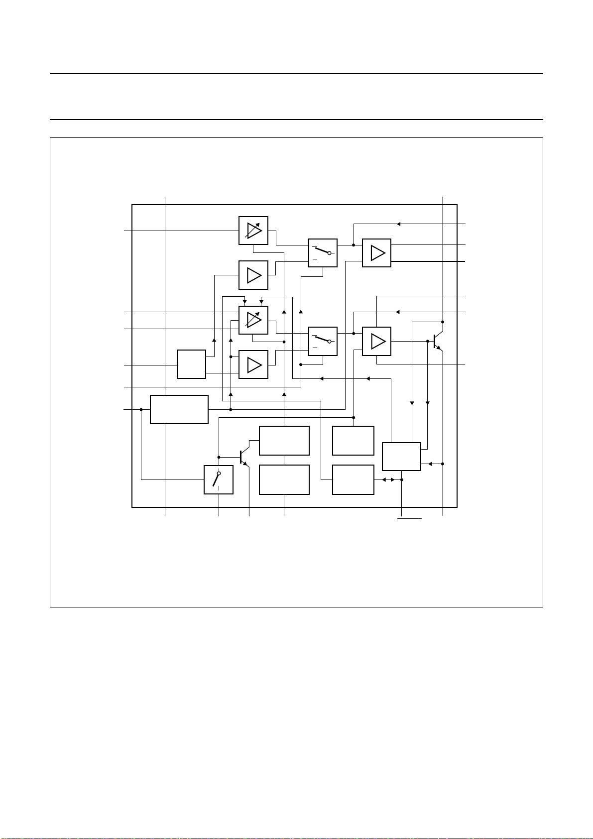
V
CC1
TEA1064A
dB
SUPPLY AND
REFERENCE
−
+
+
−
+
−
+
−
handbook, full pagewidth
IR
MIC+
MIC−
DTMF
MUTE
PD
TEA1064A
LN
116
6
GAR
5
+
−
QR+
4
QR−
19
V
CC2
2
GAS1
3
GAS2
AGC
CIRCUIT
CURRENT
REFERENCE
1711
18 10 7 20
V
EE
REG AGC STAB
LOW
VOLTAGE
CIRCUIT
START
CIRCUIT
DYNAMIC
LIMITER
DLS/MMUTE
SLPE
MGR056
Fig.1 Block diagram.
March 1994 3
Philips Semiconductors Product specification
Low voltage versatile telephone transmission circuit
with dialler interface and transmit level dynamic limiting
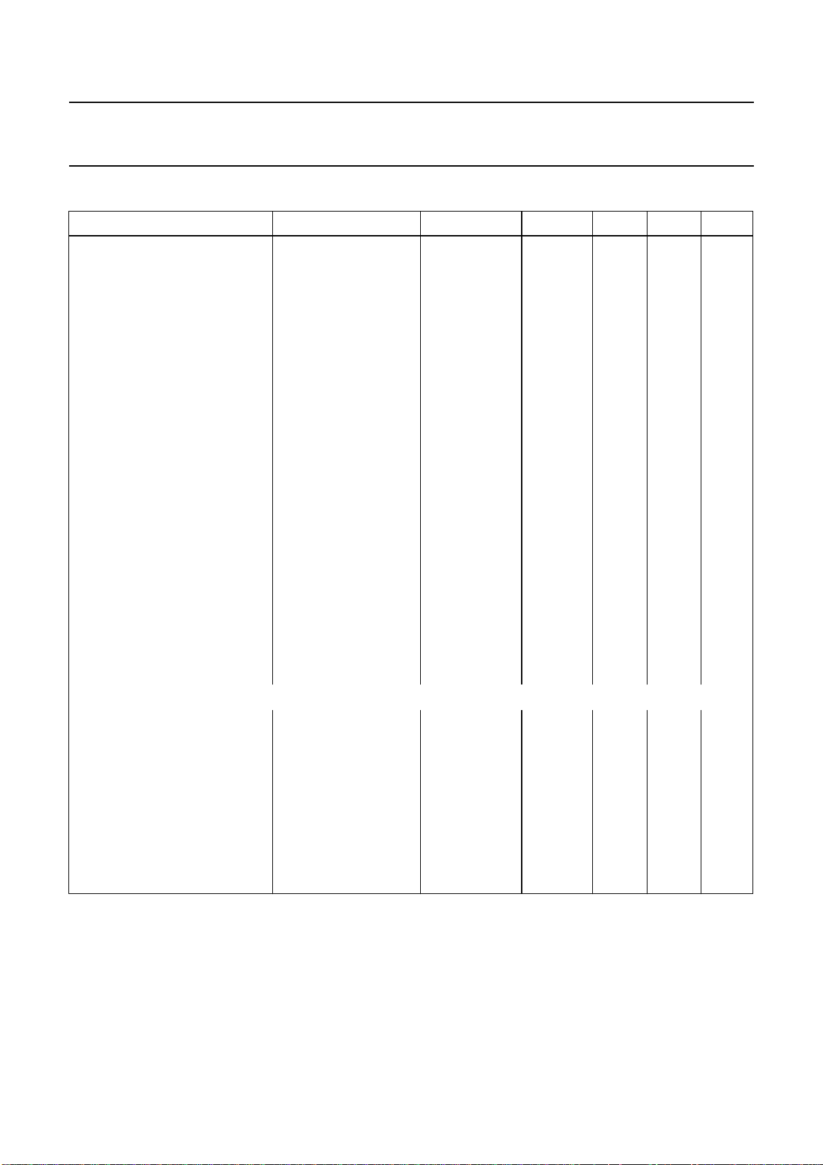
QUICK REFERENCE DATA
PARAMETER CONDITIONS SYMBOL MIN. TYP. MAX. UNIT
Operating ambient temperature
range T
Line current operating range:
normal operation l
with reduced performance l
Internal supply current:
power-down input LOW V
power-down input HIGH V
= 2.8 V I
CC1
= 2.8 V I
CC1
Voltage gain range:
microphone amplifier G
receiving amplifier G
Line loss compensation:
gain control range G
exchange supply voltage
range V
exchange feeding bridge
resistance range R
Maximum output voltage swing
on LN (peak-to-peak value) R15 + R16 = 448 Ω
l
=15mA
line
I
= 2 mA V
p
= 4 mA V
I
p
Regulated line voltage application
R15 = 0 Ω;
R16 = 392 Ω
Supply for peripherals l
DC line voltage l
=15mA
line
I
= 1.4 mA V
p
I
= 2.7 mA;
p
R
REG-SLPE
line
without R
R
REG-SLPE
=20kΩ V
=15mA
REG-SLPE
=20kΩ V
amb
line
line
CC1
CC1
v
v
v
exch
exch
LN(p-p)
LN(p-p)
p
p
V
LN
LN
TEA1064A
−25 −+75 °C
11 − 140
2 − 11 mA
− 1.3 1.6 mA
− 60 82 µA
44 − 52 dB
20 − 45 dB
5.7 6.1 6.5 dB
36 − 60 V
400 − 1000 Ω
3.7 3.95 4.2 V
3.0 3.25 3.5 V
2.5 −−V
2.9 −−V
− 3.57 − V
− 4.57 − V
(1)
mA
March 1994 4
Philips Semiconductors Product specification
Low voltage versatile telephone transmission circuit
TEA1064A
with dialler interface and transmit level dynamic limiting
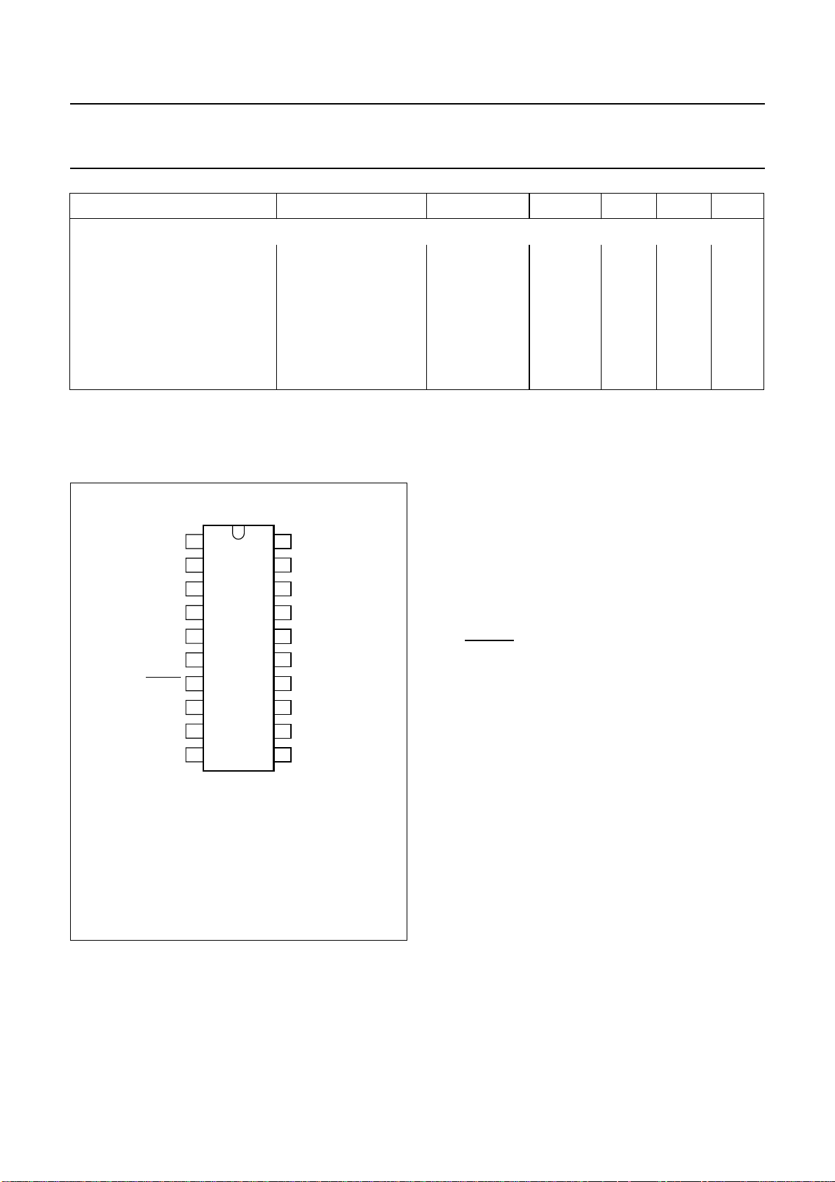
PARAMETER CONDITIONS SYMBOL MIN. TYP. MAX. UNIT
Stabilized supply voltage application
R15 = 392 Ω;
R16 = 56 Ω
Supply for peripherals l
DC line voltage l
Note
1. For TEA1064AT the maximum line current depends on the heat dissipating qualities of the mounted device.
PINNING
handbook, halfpage
DLS/MMUTE
LN
GAS1
GAS2
QR−
QR+
GAR
MIC−
MIC+
STAB
1
2
3
4
5
TEA1064A
6
7
8
9
10
MGR057
Fig.2 Pinning diagram.
= 15 mA
line
I
= 0 to 4 mA V
p
=15mA
line
I
= 2 mA V
p
I
= 4 mA V
p
SLPE
20
V
19
CC2
18
AGC
17
REG
V
16
CC1
PD
15
MUTE
14
IR
13
DTMF
12
V
11
EE
CC2-SLPE
LN
LN
3.05 3.3 3.55 V
4.2 4.4 4.8 V
4.9 5.1 5.5 V
1 LN positive line terminal
2 GAS1 gain adjustment; transmitting amplifier
3 GAS2 gain adjustment; transmitting amplifier
4QR− inverting output, receiving amplifier
5QR+ non-inverting output, receiving
amplifier
6 GAR gain adjustment; receiving amplifier
7 DLS/
MMUTE
decoupling for transmit amplifier
dynamic and microphone MUTE input
8 MIC− inverting microphone input
9 MIC+ non-inverting microphone input
10 STAB current stabilizer
11 V
EE
negative line terminal
12 DTMF dual-tone multi-frequency input
13 IR receiving amplifier input
14 MUTE mute input
15 PD power-down input
16 V
CC1
internal supply decoupling
17 REG voltage regulator decoupling
18 AGC automatic gain control input
19 V
CC2
reference voltage with respect to SLPE
20 SLPE slope adjustment for DC
curve/reference for peripheral circuits.
March 1994 5
Philips Semiconductors Product specification
Low voltage versatile telephone transmission circuit
with dialler interface and transmit level dynamic limiting
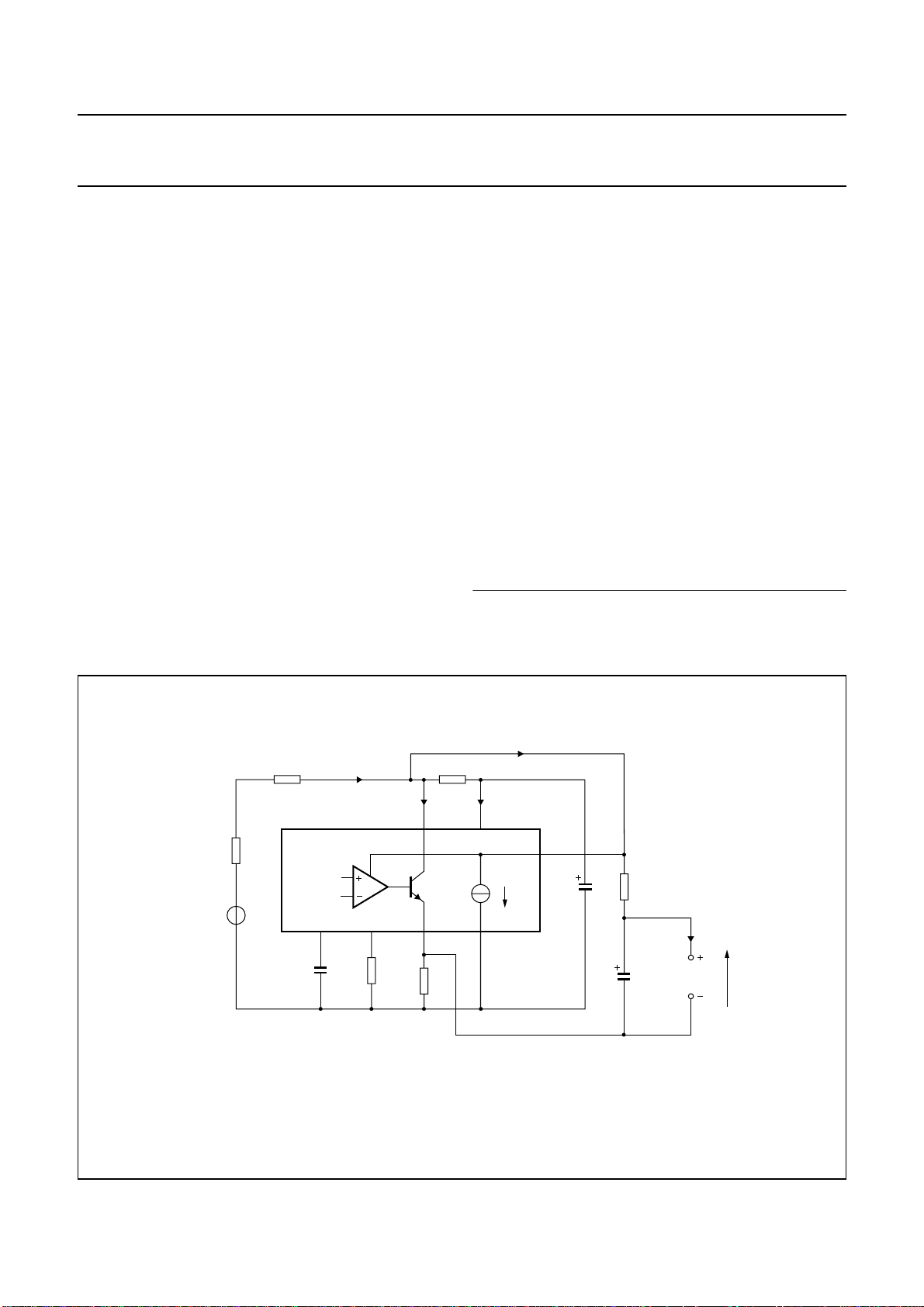
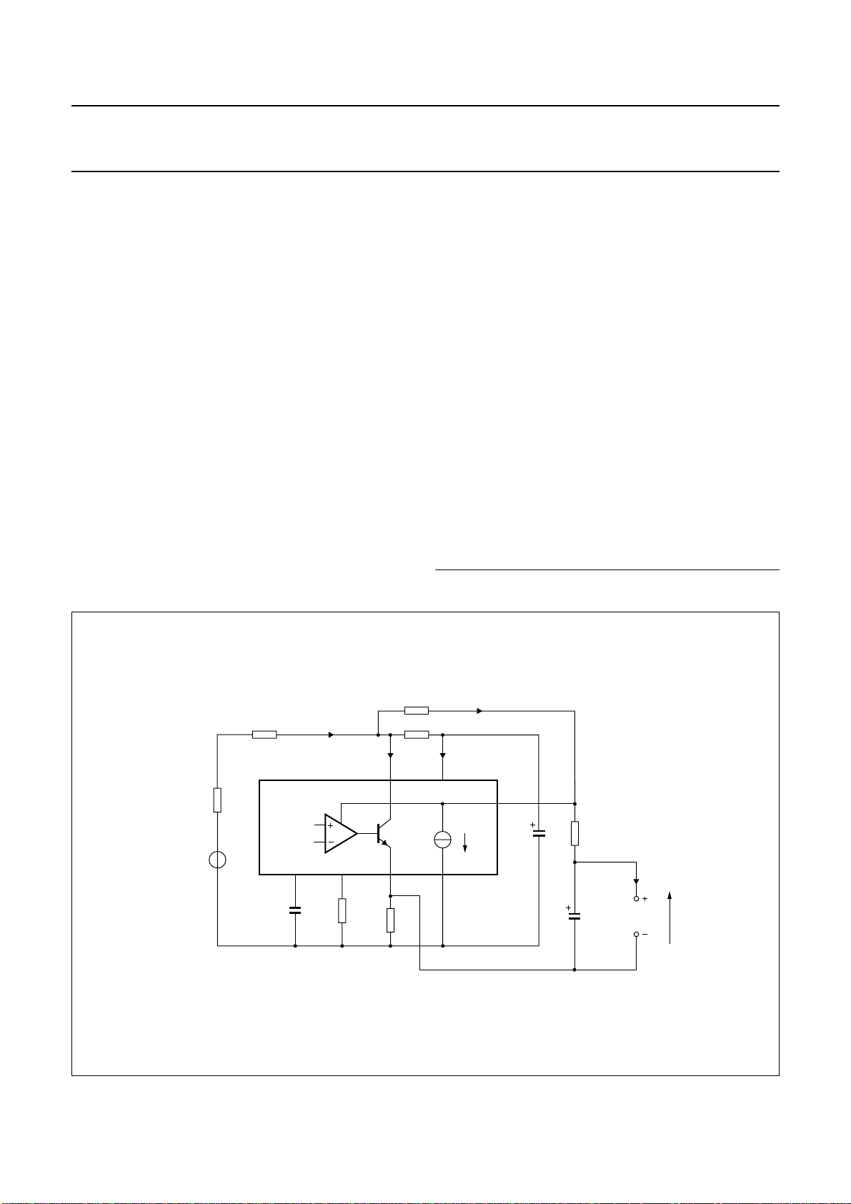
FUNCTIONAL DESCRIPTION
, V
Supplies V
CC1
, LN, SLPE, REG and STAB (Fig.3)
CC2
Power for the TEA1064A and its peripheral circuits is
usually obtained from the telephone line. The IC develops
its own supply voltage at V
and regulates its voltage
CC1
drop. The internal supply requires a decoupling capacitor
between V
and VEE. The internal current stabilizer is
CC1
set by a 3.6 kΩ resistor between STAB and VEE.
The DC current flowing into the set is determined by the
exchange supply voltage V
resistance R
, the subscriber line DC resistance R
exch
, the feeding bridge
exch
line
and the DC voltage (including polarity guard) on the
subscriber set (see Fig.3).
The internal voltage regulator generates a
temperature-compensated reference voltage that is
available between V
[V
ref=VCC2-SLPE
and SLPE
CC2
= 3.3 V (typ.)]. This internal voltage
regulator requires decoupling by a capacitor between REG
and VEE(C3).
The reference voltage can be used to:
• regulate directly the line voltage (stabilized
V
LN-SLPE=VCC2-SLPE
• to stabilize the supply voltage for peripherals.
Regulated line voltage
In this application the V
as shown in Fig.3. This configuration gives a stabilized
voltage across pins LN and SLPE which, applied via the
low-pass filter R16, C15, provides a supply to the
peripherals that is independent of the line current and
depends only on the peripheral supply current.
The value of R16 and the level of the DC voltage V
determine the supply capabilities. In the basic application
R16 = 392 Ω and C15 = 220 µF. The worst-case
peripheral supply current as a function of supply voltage is
shown in Fig.4. To increase the supply capabilities, the DC
voltage V
can be increased by using R
LN-SLPE
or by decreasing the value of R16.
(1) The TEA1064A application with regulated line voltage is the
same as is used for TEA1060/TEA1061, TEA1067 and
TEA1068 integrated circuits.
TEA1064A
(1)
)
pin is connected to the LN pin
CC2
VA(REG-SLPE)
LN-SLPE
handbook, full pagewidth
R
line
R
exch
V
exch
The voltage V
line current determine the supply capabilities and the maximum output swing on
the line (no loop damping is necessary).
The line voltage V
LN-SLPE
LN=Vref
is fixed to V
+ ([I
= 3.3± 0.25 V. Resistor R16 together with the
ref
− 1.55 mA]× R9).
line
I
line
TEA1064A
DC
AC
17
REG
C3 R5
I
SLPE
10
STAB20SLPE
LN
1
R9
Fig.3 Application with regulated line voltage (stabilized V
R1
I
CC1
Ip + 0.25 mA
V
CC1
16
0.25 mA
11
V
EE
V
19
CC2
R16C1
I
p
peripheral
C15
LN-SLPE
circuits
MGR058
).
V
p
March 1994 6
Philips Semiconductors Product specification
Low voltage versatile telephone transmission circuit
with dialler interface and transmit level dynamic limiting
The DC line voltage on LN is:
handbook, halfpage
5
I
p
(mA)
4
3
2
1
0
2
l
= 15mA; R16 = 392Ω; R15 = 0 Ω; valid for MUTE = 0 and 1.
line
Line current has very little influence
R
VA (REG-SLPE)
R
VA (REG-SLPE)
without
34
= 20 kΩ
MGR059
V
(V)
p
Fig.4 Minimum supply current for peripherals (Ip)
as a function of the peripheral supply
voltage (Vp).
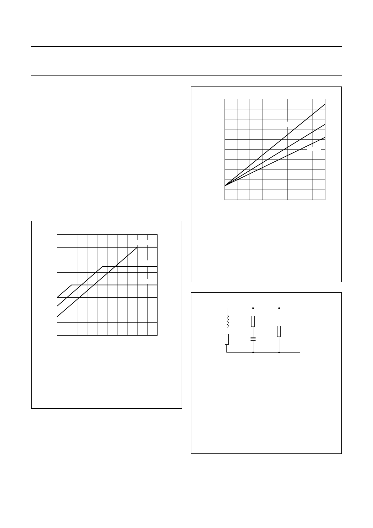
The maximum AC output swing on the line at low line
currents is influenced by R16 (limited by current) and the
maximum output swing on the line at high line currents is
influenced by the DC voltage V
LN-SLPE
(limited by voltage).
In both these situations, the internal dynamic limiter in the
sending channel prevents distortion when the microphone
input is overdriven. The maximum AC output swing on LN
is shown in Fig.5; practical values for R16 are from 200 to
600 Ω and this influences both the maximum output swing
at low line currents and the supply capabilities.
The SLPE pin is the ground reference for peripheral
circuits, therefore inputs MUTE, PD and DTMF are also
referenced to SLPE.
Active microphones can be supplied between V
CC1
and
VEE. Low-power circuits that provide only MUTE and/or PD
inputs to the TEA1064A also can be powered from V
However V
DTMF signals to the TEA1064A because V
cannot be used for circuits that provide
CC1
CC1
CC1
is referred
to ground.
VLN=V
VLN=V
LN-SLPE
+ ([I
ref
line
in which
V
= 3.3 V ± 0.25 V is the internal reference voltage
ref
between V
and SLPE; its value can be adjusted by
CC2
external resistor R
R9 = external resistor between SLPE and VEE(20 Ω in
basic application).
With R9 = 20 Ω, this results in:
VLN= 3.57 ± 0.25 V at l
VLN= 4.17 ± 0.3 V at l
R
VA(REG-SLPE)
=33kΩ
VLN= 4.57 ± 0.35 V at l
R
VA(REG-SLPE)
=20kΩ
The preferred value for R9 is 20 Ω. Changing R9
influences microphone gain, DTMF gain, the gain control
characteristics, sidetone, and the DC characteristics
(especially the low voltage characteristics).
In normal conditions, I
static behaviour is equivalent to a voltage regulator diode
with an internal resistance of R9. In the audio frequency
range the dynamic impedance is determined mainly by R1.
The equivalent impedance of the circuit in the audio
frequency range is shown in Fig.6.
The internal reference voltage V
by external resistor R
REG and SLPE. The supply voltage V
a function of R
VA(REG-SLPE)
reference voltage influences the output swing of both
sending and receiving amplifiers.
At line currents below 8 mA (typ.), the DC voltage dropped
across the circuit is adjusted to a lower level automatically
(approximately 1.8 V at 2 mA). This gives the possibility of
operating more telephone sets in parallel with DC line
voltages (excluding polarity guard) down to an absolute
minimum of 1.8 V. At line currents below 8 mA (typ.), the
circuit has limited sending and receiving levels.
.
+ (I
SLPE
− I
CC1
VA
SLPE
VA(REG-SLPE)
TEA1064A
× R9)
− 0.25 × 10⁻³A] × R9)
=15mA
line
=15mA,
line
= 15 mA,
line
>> (I
in Fig.7. Changing the
+ 0.25 mA) and the
CC1
CC2-SLPE
can be increased
connected between
CC2-SLPE
is shown as
If the line current l
exceeds I
line
+ 0.25 mA, the voltage
CC1
converter shunts the excess current to SLPE via LN;
where I
≈ 1.3 mA, the value required by the IC for
CC1
normal operation.
March 1994 7
Philips Semiconductors Product specification
Low voltage versatile telephone transmission circuit
with dialler interface and transmit level dynamic limiting
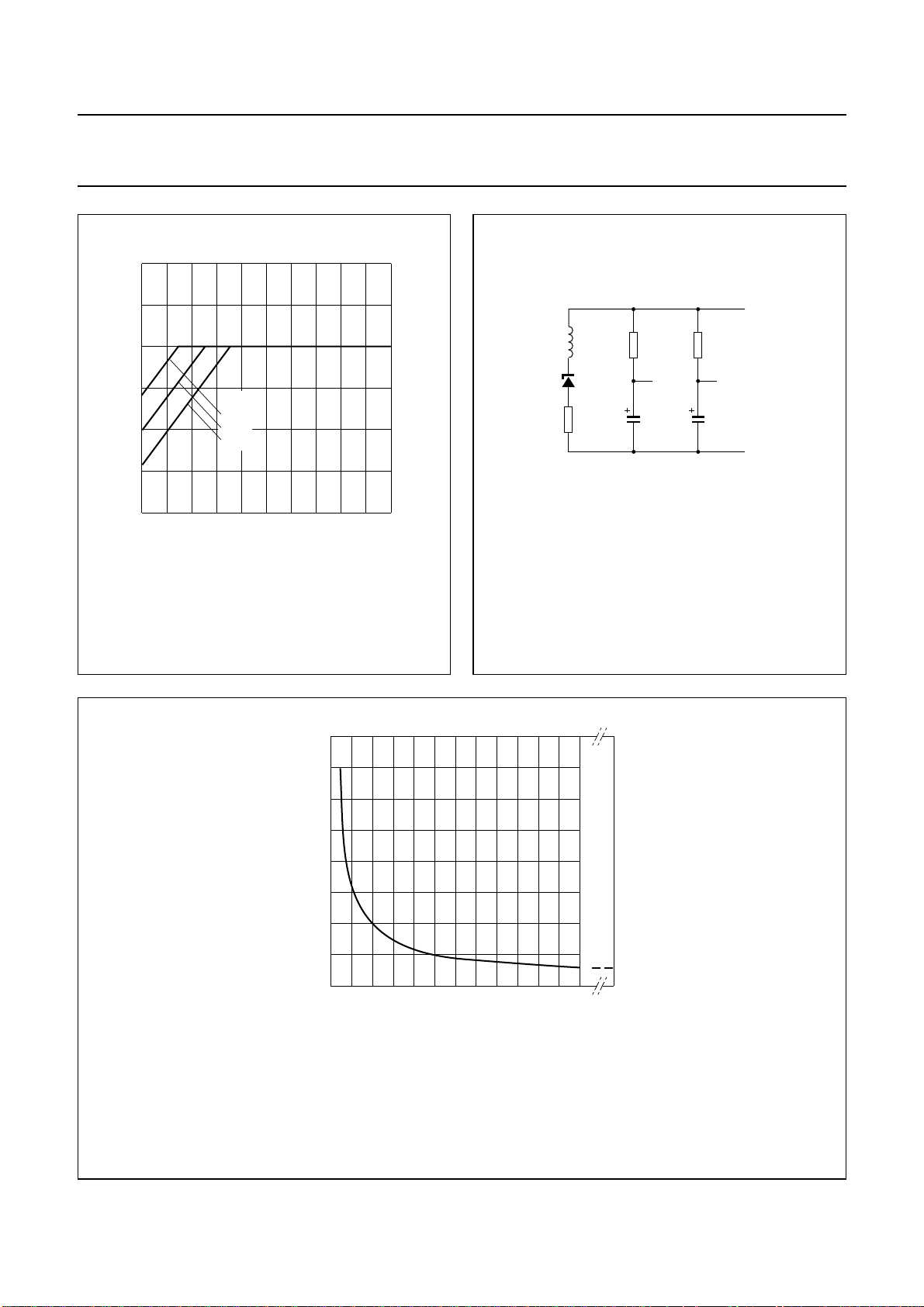
(mA)
MGR060
handbook, halfpage
L
eq
V
ref
R9
20 Ω
Fig.6 Equivalent impedance between LN and
VEEin the application with stabilized
V
LN-SLPE
R15 = 0 Ω
Leq=C3×R9 × R
Rp=15kΩ
V
LN(p-p)
(V)
6
4
Ip =
0 mA
2
0
10
2 mA
4 mA
20 30
I
line
handbook, halfpage
Fig.5 Maximum AC output swing on the line as a
function of line current with peripheral
supply current as a parameter: R15 = 0 Ω;
R16 = 392 Ω.
TEA1064A
LN
R
p
REG
C3
4.7 µF
:
R1
V
CC1
C1
V
MGR061
p
EE
handbook, full pagewidth
Fig.7 Internal reference voltage V
and 140 mA.
In the stabilized supply application:
VLN=V
CC2-SLPE
+ ([Ip+ 0.25 × 10⁻³A] × R15) + ([I
In the unregulated supply application (R15 = 0 Ω):
VLN=V
CC2-SLPE
+ ([I
7.8
V
ref
(V)
6.6
5.4
4.2
3.0
08040 120
CC2-SLPE
− 1.55 × 10⁻³A] × R9)
line
as a function of resistor R
RVA (REG-SLPE) (kΩ)
− 1.55 × 10⁻³A] × R9)
line
MGR062
VA(REG-SLPE)
with R
VA
infinite
for line currents between 11
March 1994 8
Philips Semiconductors Product specification
Low voltage versatile telephone transmission circuit
with dialler interface and transmit level dynamic limiting
Stabilized peripheral supply voltage
The configuration shown in Fig.8 provides a stabilized
voltage across pins V
and SLPE for peripheral circuits
CC2
(such as dialling and control circuits); the DC voltage
VLNnow varies with the peripheral supply current.
The V
CC2-SLPE
supply must be decoupled by capacitor
C15. For stable loop operation, resistor R16 (≈ 50 Ω) is
connected between V
and SLPE in series with C15.
CC2
The voltage regulator control loop is completed by resistor
R15 between LN and V
CC2
.
For sets with an impedance of 600 Ω, practical values are:
R15 = 200 to 600 Ω; C15 = 220 µF; C3 = 470 nF. The
ratio R15/R16 ≤ 8 is for stable loop operation with
sufficient phase margin, and R15/R16 ≥ 6 is for
satisfactory set impedance in the audio frequency range.
For sets with complex impedance, the value of C3 and the
ratio R15/R16 are different (further information is given in
the TEA1064A Application Report
(1)
).
the values of external components (especially R15). With
R15 = 392 Ω and R16 = 56 Ω (basic application) the
maximum possible AC output swing on the line as a
function of line current is as shown in Fig.9, the curve
parameter is the peripheral supply current (Ip). Different
values for R15 (from 200 to 600 Ω) maintaining
6 < R15/R16 < 8 give different results (these are described
in the TEA1064A Application Report
TEA1064A
(1)
.
The peripheral supply capability depends mainly on the
available line current, the required AC output swing on the
line, the maximum permitted DC voltage on the line and
handbook, full pagewidth
V
R
exch
exch
R
line
I
line
TEA1064A
DC
AC
17
REG
C3 R5
I
SLPE
10
STAB20SLPE
LN
1
R9
(1) Supplied on request.
R1
I
CC1
Ip + 0.25 mA
V
CC1
16
0.25 mA
11
V
EE
19
R15
V
CC2
R16C1
C15
I
p
peripheral
circuits
V
p
Fig.8 Application with stabilized supply voltage for peripheral circuits: R15 = 392 Ω; R16 = 56 Ω.
March 1994 9
MGR063
Philips Semiconductors Product specification
Low voltage versatile telephone transmission circuit
with dialler interface and transmit level dynamic limiting
The DC line voltage on LN is
VLN=V
LN-SLPE
+ (I
SLPE
× R9).
Therefore
VLN=V
+ ([Ip+ 0.25 × 10⁻³A] × R15) +
ref
([l
− I
line
− 0.25 × 10⁻³A] × R9)
CC1
in which:
V
is the internal reference voltage between V
ref
SLPE (the value of V
resistor, RVA). V
ref
can be adjusted by an external
ref
= 3.3 V (typ.) without R
VA
Ipis the supply current used by peripheral circuits
R15 is an external resistor between LN and V
in the basic application)
R9 is an external resistor between SLPE and
VEE(20 Ω in the basic application)
MGR064
Ip = 4 mA
2 mA
0 mA
V
LN(p-p)
(V)
8
6
4
handbook, halfpage
CC2
CC2
(392 Ω
and
5.5
handbook, halfpage
V
LN-SLPE
(V)
5.0
4.5
4.0
3.5
3.0
012 4
V
changing the value of R
The total voltage drop V
can be adjusted between approximately 3.3 and 4.3 V by
CC2-SLPE
Fig.10 Curves showing the typical voltage drop
between LN and SLPE as a function of the
supply current for peripherals with R15 as a
parameter: V
connected).
TEA1064A
MGR065
R15 = 511 Ω
392 Ω
301 Ω
3
Ip (mA)
, this results in a parallel-shift of the curves.
VA
≈ V
LN
CC2-SLPE
+ ([I
LN-SLPE
= 3.3 V (RVAnot
− 1.55 mA] × R9).
line
2
0
10
As different values of R15 and R16 are allowed, different curves
would then apply
20 30
I
(mA)
line
Fig.9 Maximum output swing on line as a function
of line current with the peripheral supply
current as a parameter; R15 = 392 Ω;
R16 = 56 Ω.
The DC voltage V
LN-SLPE
as a function of Ipwith R15 as a
parameter is shown in Fig.10. In the audio frequency
range, the dynamic impedance is determined mainly by
R1. The equivalent impedance in the audio range of the
circuit (Fig.8) is shown in Fig.11.
March 1994 10
MGR066
LN
V
handbook, halfpage
=
ReqR
p
LeqC3 R9× Reqwith Rp15 kΩ=×=
L
eq
R9
20 Ω
R15
----------- 1+
R16
R
eq
C3
470 nF
R1
620 Ω
Fig.11 Equivalent impedance between LN and
VEEat f > 300 Hz in the application with
stabilized supply voltage for peripheral
circuits.
EE
Philips Semiconductors Product specification
Low voltage versatile telephone transmission circuit
with dialler interface and transmit level dynamic limiting
Microphone inputs MIC+ and MIC− and gain pins
GAS1 and GAS2
The TEA1064A has symmetrical microphone inputs, its
input impedance is 64 kΩ (2 × 32 kΩ) and its voltage
amplification is typ. 52 dB with R7 = 68 kΩ. Either
dynamic, magnetic or piezo-electric microphones can be
used, or an electret microphone with a built-in FET buffer.
Arrangements for the microphone types are shown in
Fig.12.
handbook, full pagewidth
MIC+
9
(1)
MIC−
8
The gain of the microphone amplifier is proportional to
external resistor R7 connected between GAS1 and GAS2
and with this it can be adjusted between 44 dB and 52 dB
to suit the sensitivity of the transducer.
An external 100 pF capacitor (C6) is required between
GAS1 and SLPE to ensure stability. A larger value of C6
may be chosen to obtain a first-order low-pass filter with a
cut-off frequency corresponding to the time constant
R7 × C6.
V
CC1
MIC−
MIC+
16
8
9
11
V
EE
TEA1064A
MIC+
9
MIC−
8
MGR067
(a) (b)
(c)
Fig.12 Microphone arrangements: a) magnetic or dynamic microphone, the resistor (1) may be connected to
reduce the terminating impedance, or for sensitive types a resistive attenuator can be used to prevent
overloading the microphone inputs; b) electret microphone; c) piezo-electric microphone.
Dynamic limiter (microphone) pin DLS/MMUTE
A low level at the DLS/MMUTE pin inhibits the microphone
inputs MIC+ and MIC− but has no influence on the
receiving and DTMF amplifiers.
Removing the low level at the DLS/MMUTE pin provides
the normal function of the microphone amplifier after a
means that the maximum output swing on the line will be
higher if the DC voltage dropped across the circuit is
increased.
Fig.14 shows the maximum possible output swing on the
line as a function of the DC voltage drop (V
I
− Ipas a parameter.
line
short time determined by the capacitor connected to
DLS/MMUTE pin. The microphone mute function can be
realised by a simple switch as shown in Fig.13.
To prevent distortion of the transmitted signal, the gain of
the sending amplifier is reduced rapidly when peaks of the
signal on the line exceed an internally-determined
threshold. The time in which gain reduction is effected
handbook, halfpage
R17
3.3 kΩ
DLS/MMUTE
7
(attack time) is very short. The circuit stays in the
gain-reduced condition until the peaks of the sending
signal remain below the threshold level. The sending gain
V
EE
11
then returns to normal after a time determined by the
capacitor connected to DLS/MMUTE (release time).
MGR068
LN-SLPE
) with
The internal threshold adapts automatically to the DC
voltage setting of the circuit (voltage V
LN-SLPE
). This
March 1994 11
Fig.13 Microphone-mute function.
 Loading...