

Philips TEA1062T, TEA1062A, TEA1062, TEA1062M1, TEA1062AT Datasheet
...
INTEGRATED CIRCUITS
DATA SH EET
TEA1062; TEA1062A
Low voltage transmission circuits
with dialler interface
Product specification
Supersedes data of 1996 Dec 04
File under Integrated Circuits, IC03
1997 Sep 03
Philips Semiconductors Product specification
Low voltage transmission circuits with
dialler interface
FEATURES
• Low DC line voltage; operates down to 1.6 V (excluding
polarity guard)
• Voltage regulator with adjustable static resistance
• Provides a supply for external circuits
• Symmetrical high-impedance inputs (64 kΩ) for
dynamic, magnetic or piezoelectric microphones
• Asymmetrical high-impedance input (32 kΩ) for electret
microphones
• DTMF signal input with confidence tone
• Mute input for pulse or DTMF dialling
– TEA1062: active HIGH (MUTE)
– TEA1062A: active LOW (
• Receiving amplifier for dynamic, magnetic or
piezoelectric earpieces
• Large gain setting ranges on microphone and earpiece
amplifiers
• Line loss compensation (line current dependent) for
microphone and earpiece amplifiers
• Gain control curve adaptable to exchange supply
• DC line voltage adjustment facility.
MUTE)
TEA1062; TEA1062A
GENERAL DESCRIPTION
The TEA1062 and TEA1062A are integrated circuits that
perform all speech and line interface functions required in
fully electronic telephone sets. They perform electronic
switching between dialling and speech. The ICs operate at
line voltage down to 1.6 V DC (with reduced performance)
to facilitate the use of more telephone sets connected in
parallel.
All statements and values refer to all versions unless
otherwise specified.
QUICK REFERENCE DATA
SYMBOL PARAMETER CONDITIONS MIN. TYP. MAX. UNIT
V
I
line
LN
line voltage I
operating line current
= 15 mA 3.55 4.0 4.25 V
line
normal operation 11 − 140 mA
with reduced performance 1 − 11 mA
I
CC
V
CC
G
v
internal supply current VCC= 2.8 V − 0.9 1.35 mA
supply voltage for peripherals I
TEA1062 I
TEA1062A I
=15mA
line
= 1.2 mA; MUTE = HIGH 2.2 2.7 − V
p
I
= 0 mA; MUTE = HIGH − 3.4 − V
p
= 1.2 mA; MUTE = LOW 2.2 2.7 − V
p
= 0 mA; MUTE = LOW − 3.4 − V
I
p
voltage gain
microphone amplifier 44 − 52 dB
receiving amplifier 20 − 31 dB
T
amb
operating ambient temperature −25 − +75 °C
Line loss compensation
∆G
V
R
v
exch
exch
gain control − 5.8 − dB
exchange supply voltage 36 − 60 V
exchange feeding bridge resistance 0.4 − 1kΩ
1997 Sep 03 2
Philips Semiconductors Product specification
Low voltage transmission circuits with
TEA1062; TEA1062A
dialler interface
ORDERING INFORMATION
TYPE NUMBER
NAME DESCRIPTION VERSION
TEA1062 DIP16 plastic dual in-line package; 16 leads (300 mil) SOT38-1
TEA1062M1 DIP16 plastic dual in-line package; 16 leads (300 mil) SOT38-4 or
TEA1062A DIP16 plastic dual in-line package; 16 leads (300 mil) SOT38-1
TEA1062AM1 DIP16 plastic dual in-line package; 16 leads (300 mil) SOT38-4 or
TEA1062T SO16 plastic small outline package; 16 leads; body width 3.9 mm SOT109-1
TEA1062A T SO16 plastic small outline package; 16 leads; body width 3.9 mm SOT109-1
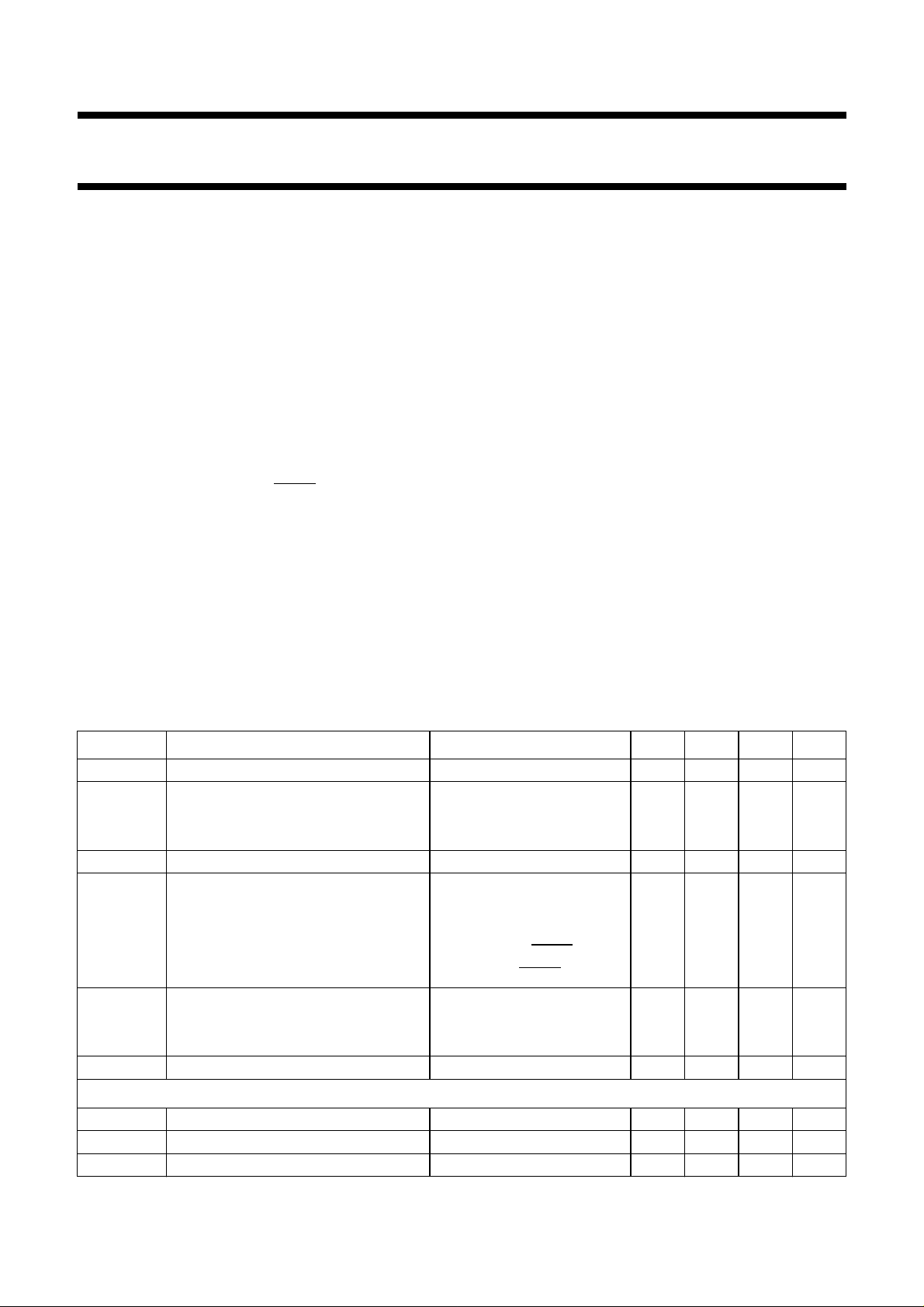
BLOCK DIAGRAM
V
CC
handbook, full pagewidth
10
IR
13
PACKAGE
LN
1
5
SOT38-9
SOT38-9
GAR
(1)
MIC
MIC
DTMF
MUTE
7
6
11
12
SUPPLY AND
REFERENCE
TEA1062A
dB
CONTROL
CURRENT
CURRENT
REFERENCE
91415 8 16
EE
LOW VOLTAGE
CIRCUIT
4
2
3
MBA359 - 1
SLPESTABAGCREGV
QR
GAS1
GAS2
(1) Pin 12 is active HIGH (MUTE) for TEA1062.
Fig.1 Block diagram for TEA1062A.
1997 Sep 03 3
Philips Semiconductors Product specification
Low voltage transmission circuits with
dialler interface
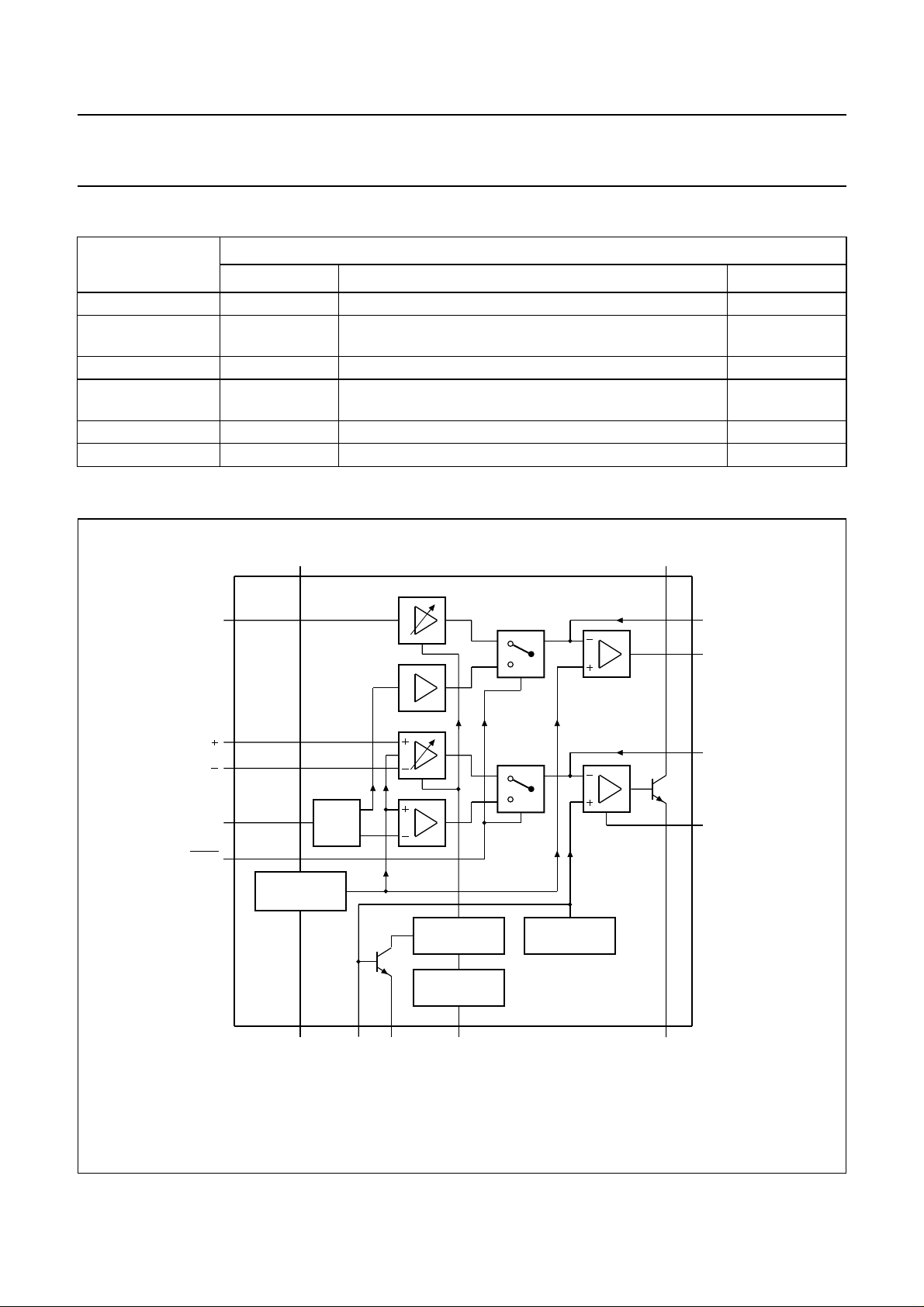
PINNING
SYMBOL PIN DESCRIPTION
LN 1 positive line terminal
GAS1 2 gain adjustment; transmitting
amplifier
GAS2 3 gain adjustment; transmitting
amplifier
QR 4 non-inverting output; receiving
amplifier
GAR 5 gain adjustment; receiving
amplifier
MIC− 6 inverting microphone input
MIC+ 7 non-inverting microphone input
STAB 8 current stabilizer
V
EE
IR 10 receiving amplifier input
DTMF 11 dual-tone multi-frequency input
MUTE 12 mute input (see note 1)
V
CC
REG 14 voltage regulator decoupling
AGC 15 automatic gain control input
SLPE 16 slope (DC resistance) adjustment
9 negative line terminal
13 positive supply decoupling
handbook, halfpage
Fig.2 Pin configuration for TEA1062A.
GAS1
GAS2
QR
GAR
MIC
MIC
STAB
TEA1062; TEA1062A
LN
1
2
3
4
5
6
7
8
TEA1062A
MBA354 - 1
16
15
14
13
12
11
10
9
SLPE
AGC
REG
V
CC
MUTE
DTMF
IR
V
EE
Note
1. Pin 12 is active HIGH (MUTE) for TEA1062.
1997 Sep 03 4
Philips Semiconductors Product specification
Low voltage transmission circuits with
dialler interface
FUNCTIONAL DESCRIPTION
Supplies V
Power for the IC and its peripheral circuits is usually
obtained from the telephone line. The supply voltage is
derived from the line via a dropping resistor and regulated
by the IC. The supply voltage V
supply external circuits e.g. dialling and control circuits.
Decoupling of the supply voltage is performed by a
capacitor between VCC and VEE. The internal voltage
regulator is decoupled by a capacitor between REG and
VEE.
The DC current flowing into the set is determined by the
exchange supply voltage V
resistance R
line R
line
The circuit has an internal current stabilizer operating at a
level determined by a 3.6 kΩ resistor connected between
STAB and VEE (see Fig.9). When the line current (I
more than 0.5 mA greater than the sum of the IC supply
current (ICC) and the current drawn by the peripheral
circuitry connected to VCC (Ip) the excess current is
shunted to VEE via LN.
The regulated voltage on the line terminal (VLN) can be
calculated as:
VLN=V
VLN=V
V
is an internally generated temperature compensated
ref
reference voltage of 3.7 V and R9 is an external resistor
connected between SLPE and VEE.
In normal use the value of R9 would be 20 Ω.
Changing the value of R9 will also affect microphone gain,
DTMF gain, gain control characteristics, sidetone level,
maximum output swing on LN and the DC characteristics
(especially at the lower voltages).
Under normal conditions, when I
the static behaviour of the circuit is that of a 3.7 V regulator
diode with an internal resistance equal to that of R9. In the
audio frequency range the dynamic impedance is largely
determined by R1. Fig.3 shows the equivalent impedance
of the circuit.
, LN, SLPE, REG and STAB
CC
exch
and the DC resistance of the telephone
exch
.
ref+ISLPE
+ {(I
ref
× R9
− ICC− 0.5 × 10⁻³A) − Ip} × R9
line
may also be used to
CC
, the feeding bridge
>> ICC + 0.5 mA + Ip,
SLPE
line
) is
TEA1062; TEA1062A
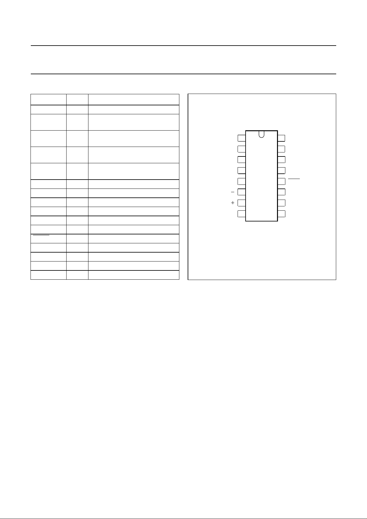
handbook, halfpage
Leq=C3×R9 × Rp.
Rp= 16.2 kΩ.
At line currents below 9 mA the internal reference voltage
is automatically adjusted to a lower value (typically 1.6 V
at 1 mA). This means that more sets can be operated in
parallel with DC line voltages (excluding the polarity guard)
down to an absolute minimum voltage of 1.6 V. At line
currents below 9 mA the circuit has limited sending and
receiving levels. The internal reference voltage can be
adjusted by means of an external resistor (R
This resistor when connected between LN and REG will
decrease the internal reference voltage and when
connected between REG and SLPE will increase the
internal reference voltage.
Current (Ip) available from VCC for peripheral circuits
depends on the external components used. Fig.10 shows
this current for VCC> 2.2 V. If MUTE is LOW (TEA1062) or
MUTE is HIGH (TEA1062A) when the receiving amplifier
is driven, the available current is further reduced. Current
availability can be increased by connecting the supply IC
(TEA1081) in parallel with R1 as shown in Fig.19 and
Fig.20, or by increasing the DC line voltage by means of
an external resistor (RVA) connected between REG and
SLPE (Fig.18).
LN
L
eq
V
R9
20 Ω
V
EE
ref
R
REG
p
C3
4.7 µF C1100 µF
R1
V
CC
MBA454
Fig.3 Equivalent impedance circuit.
VA
).
1997 Sep 03 5

Philips Semiconductors Product specification
Low voltage transmission circuits with
dialler interface
Microphone inputs MIC+ and MIC− and gain pins
GAS1 and GAS2
The circuit has symmetrical microphone inputs. Its input
impedance is 64 kΩ (2 × 32 kΩ) and its voltage gain is
typically 52 dB (when R7 = 68 kΩ, see Figures 14
and 15). Dynamic, magnetic, piezoelectric or electret (with
built-in FET source followers) can be used. Microphone
arrangements are illustrated in Fig.11.
The gain of the microphone amplifier can be adjusted
between 44 dB and 52 dB to suit the sensitivity of the
transducer in use. The gain is proportional to the value of
R7 which is connected between GAS1 and GAS2.
Stability is ensured by two external capacitors, C6
connected between GAS1 and SLPE and C8 connected
between GAS1 and V
may be increased to obtain a first-order low-pass filter.
The value of C8 is 10 times the value of C6. The cut-off
frequency corresponds to the time constant R7 × C6.
. The value of C6 is 100 pF but this
EE
TEA1062; TEA1062A
Receiving amplifier IR, QR and GAR
The receiving amplifier has one input (IR) and a
non-inverting output (QR). Earpiece arrangements are
illustrated in Fig.12. The IR to QR gain is typically 31 dB
(when R4 = 100 kΩ). It can be adjusted between
20 and 31 dB to match the sensitivity of the transducer in
use. The gain is set with the value of R4 which is
connected between GAR and QR. The overall receive
gain, between LN and QR, is calculated by subtracting the
anti-sidetone network attenuation (32 dB) from the
amplifier gain. Two external capacitors, C4 and C7, ensure
stability. C4 is normally 100 pF and C7 is 10 times the
value of C4. The value of C4 may be increased to obtain a
first-order low-pass filter. The cut-off frequency will depend
on the time constant R4 × C4.
The output voltage of the receiving amplifier is specified for
continuous-wave drive. The maximum output voltage will
be higher under speech conditions where the peak to RMS
ratio is higher.
Input MUTE (TEA1062)
When MUTE is HIGH the DTMF input is enabled and the
microphone and receiving amplifier inputs are inhibited.
The reverse is true when MUTE is LOW or open-circuit.
MUTE switching causes only negligible clicking on the line
and earpiece output. If the number of parallel sets in use
causes a drop in line current to below 6 mA the speech
amplifiers remain active independent to the DC level
applied to the MUTE input.
Input MUTE (TEA1062A)
When MUTE is LOW or open-circuit, the DTMF input is
enabled and the microphone and receiving amplifier inputs
are inhibited. The reverse is true when MUTE is HIGH.
MUTE switching causes only negligible clicking on the line
and earpiece output. If the number of parallel sets in use
causes a drop in line current to below 6 mA the DTMF
amplifier becomes active independent to the DC level
applied to the MUTE input.
Dual-tone multi-frequency input DTMF
When the DTMF input is enabled dialling tones may be
sent on to the line. The voltage gain from DTMF to LN is
typically 25.5 dB (when R7 = 68 kΩ) and varies with R7 in
the same way as the microphone gain. The signalling
tones can be heard in the earpiece at a low level
(confidence tone).
Automatic Gain Control input AGC
Automatic line loss compensation is achieved by
connecting a resistor (R6) between AGC and V
The automatic gain control varies the gain of the
microphone amplifier and the receiving amplifier in
accordance with the DC line current. The control range is
5.8 dB which corresponds to a line length of 5 km for a
0.5 mm diameter twisted-pair copper cable with a DC
resistance of 176 Ω/km and average attenuation of
1.2 dB/km). Resistor R6 should be chosen in accordance
with the exchange supply voltage and its feeding bridge
resistance (see Fig.13 and Table 1). The ratio of start and
stop currents of the AGC curve is independent of the value
of R6. If no automatic line-loss compensation is required
the AGC pin may be left open-circuit. The amplifiers, in this
condition, will give their maximum specified gain.
EE
.
1997 Sep 03 6

Philips Semiconductors Product specification
Low voltage transmission circuits with
dialler interface
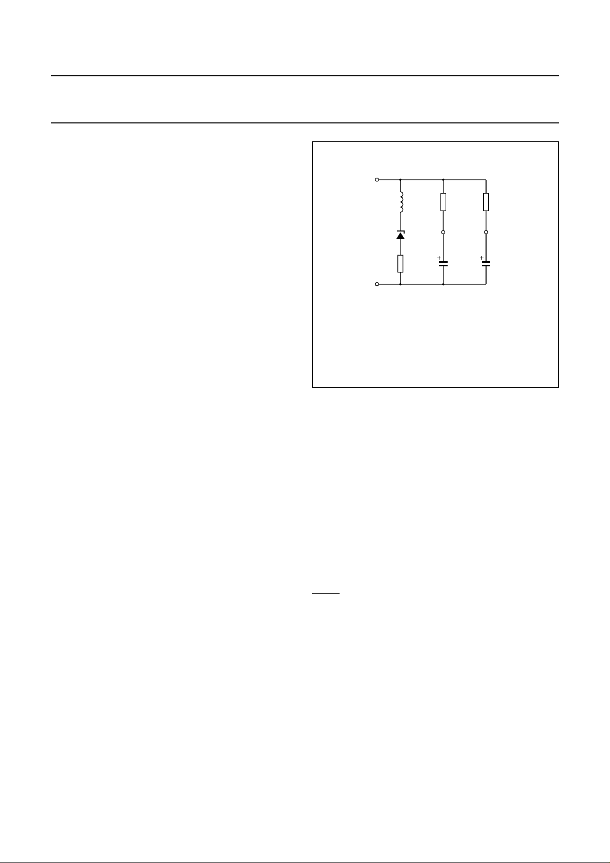
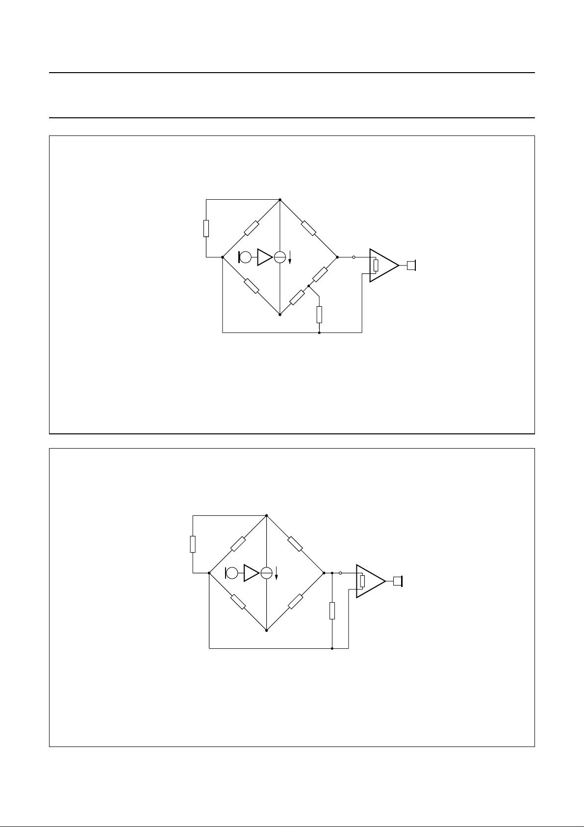
Sidetone suppression
The anti-sidetone network, R1//Z
Z
, (see Fig.4) suppresses the transmitted signal in the
bal
earpiece. Maximum compensation is obtained when the
following conditions are fulfilled:
R9 R2× R1 R3
------------------------ Z
bal
×=
Z
bal
=
R8+
If fixed values are chosen for R1, R2, R3 and R9, then
condition (1) will always be fulfilled when |R8//Z
To obtain optimum sidetone suppression, condition (2) has
to be fulfilled which results in:
R8
Z
bal
Where k is a scale factor;
------- R1
Z
line
kZ
×=×=
line
k
The scale factor k, dependent on the value of R8, is
chosen to meet the following criteria:
• compatibility with a standard capacitor from the E6 or
E12 range for Z
•Z
//R8 << R3 fulfilling condition (a) and thus
bal
bal
ensuring correct anti-sidetone bridge operation
•Z
+ R8 >> R9 to avoid influencing the transmit gain.
bal
In practise Z
varies considerably with the line type and
line
length. The value chosen for Z
an average line length thus giving optimum setting for
short or long lines.
, R2, R3, R8, R9 and
line
×
R8 Z
+
Z
line
-------------------------Z
line
R8
=
------- R1
should therefore be for
bal
bal
------------------------ -
+
R8 Z
bal
R1+
| << R3.
bal
(1)
(2)
TEA1062; TEA1062A
E
XAMPLE
The balance impedance Z
suppression is present can be calculated by:
Suppose Z
= 210 Ω + (1265 Ω//140 nF) representing a
line
5 km line of 0.5 mm diameter, copper, twisted-pair cable
matched to 600 Ω (176 Ω/km; 38 nF/km).
When k = 0.64 then R8 = 390 Ω;
Z
= 130 Ω + (820 Ω//220 nF).
bal
The anti-sidetone network for the TEA1060 family shown
in Fig.4 attenuates the signal received from the line by
32 dB before it enters the receiving amplifier.
The attenuation is almost constant over the whole
audio-frequency range.
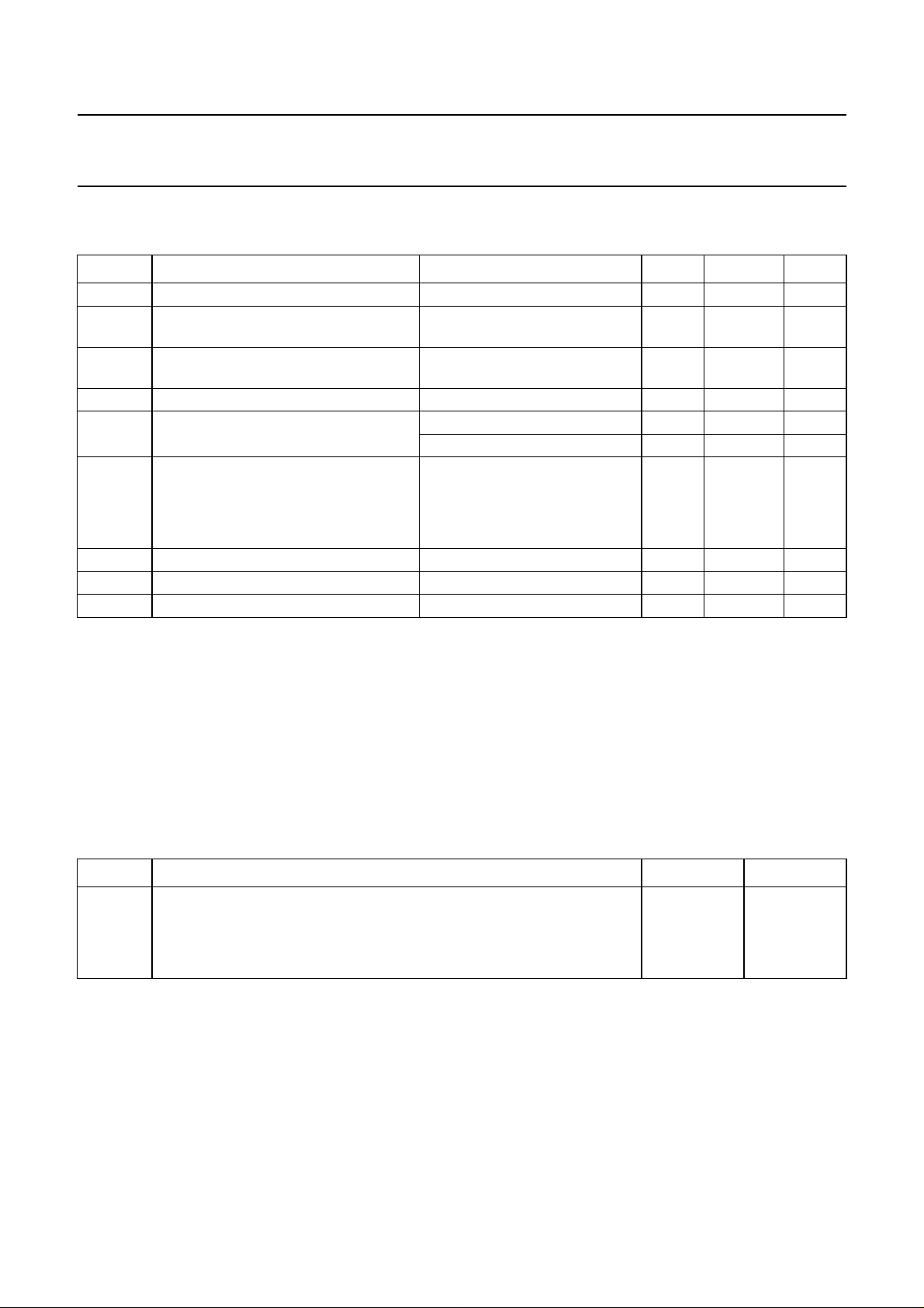
Figure 5 shows a conventional Wheatstone bridge
anti-sidetone circuit that can be used as an alternative.
Both bridge types can be used with either resistive or
complex set impedances. (More information on the
balancing of anti-sidetone bridges can be obtained in our
publication
systems, IC03b”
“Applications Handbook for Wired telecom
, order number 9397 750 00811.)
at which the optimum
bal
1997 Sep 03 7
Philips Semiconductors Product specification
Low voltage transmission circuits with
dialler interface
LN
handbook, full pagewidth
Z
line
V
EE
R1 R2
R9
SLPE
TEA1062; TEA1062A
R3
IR
R
t
Z
bal
MSA500 - 1
i
m
R8
ok, full pagewidth
Fig.4 Equivalent circuit of TEA1060 family anti-sidetone bridge.
LN
Z
line
V
EE
R1
R9
SLPE
Z
bal
i
m
R8
IR
R
t
R
A
MSA501 - 1
Fig.5 Equivalent circuit of an anti-sidetone network in a Wheatstone bridge configuration.
1997 Sep 03 8
Philips Semiconductors Product specification
Low voltage transmission circuits with
TEA1062; TEA1062A
dialler interface
LIMITING VALUES
In accordance with the Absolute Maximum Rating System (IEC 134).
SYMBOL PARAMETER CONDITIONS MIN. MAX. UNIT
V
LN
V
LN(R)
V
LN(RM)
I
line
V
I
P
tot
T
amb
T
stg
T
j
positive continuous line voltage − 12 V
repetitive line voltage during switch-on
− 13.2 V
or line interruption
repetitive peak line voltage for a 1 ms
pulse per 5 s
R9 = 20 Ω; R10 = 13 Ω;
see Fig.18
− 28 V
line current R9 = 20 Ω; note 1 − 140 mA
input voltage on all other pins positive input voltage − VCC+ 0.7 V
negative input voltage −−0.7 V
total power dissipation R9 = 20 Ω; note 2
TEA1062; TEA1062A − 666 mW
TEA1062M1; TEA1062AM1 − 617 mW
TEA1062T; TEA1062AT − 454 mW
operating ambient temperature −25 +75 °C
storage temperature −40 +125 °C
junction temperature − 125 °C
Notes
1. Mostly dependent on the maximum required T
2. Calculated for the maximum ambient temperature specified (T
and on the voltage between LN and SLPE (see Figs 6, 7 and 8).
amb
=75°C) and a maximum junction temperature of
amb
125 °C.
HANDLING
This device meets class 2 ESD test requirements [Human Body Model (HBM)], in accordance with
“MIL STD 883C - method 3015”
.
THERMAL CHARACTERISTICS
SYMBOL PARAMETER VALUE UNIT
R
th j-a
thermal resistance from junction to ambient in free air
TEA1062; TEA1062A 75 K/W
TEA1062M1; TEA1062AM1 81 K/W
TEA1062T; TEA1062AT (note 1) 110 K/W
Note
1. Mounted on glass epoxy board 28.5 × 19.1 × 1.5 mm.
1997 Sep 03 9
 Loading...