

Philips TEA1039 Datasheet

INTEGRATED CIRCUITS
DATA SH EET
TEA1039
Control circuit for switched-mode
power supply
Product specification
File under Integrated Circuits, IC02
August 1982

Philips Semiconductors Product specification
Control circuit for switched-mode power supply TEA1039
GENERAL DESCRIPTION
The TEA1039 is a bipolar integrated circuit intended for the control of a switched-mode power supply. Together with an
external error amplifier and a voltage regulator (e.g. a regulator diode) it forms a complete control system. The circuit is
capable of directly driving the SMPS power transistor in small SMPS systems.
It has the following features:
• Suited for frequency and duty factor regulation.
• Suited for flyback converters and forward converters.
• Wide frequency range.
• Adjustable input sensitivity.
• Adjustable minimum frequency or maximum duty factor limit.
• Adjustable overcurrent protection limit.
• Supply voltage out-of-range protection.
• Slow-start facility.
QUICK REFERENCE DATA
Supply voltage V
Supply current I
Output pulse repetition frequency range f
Output current LOW I
Operating ambient temperature range T
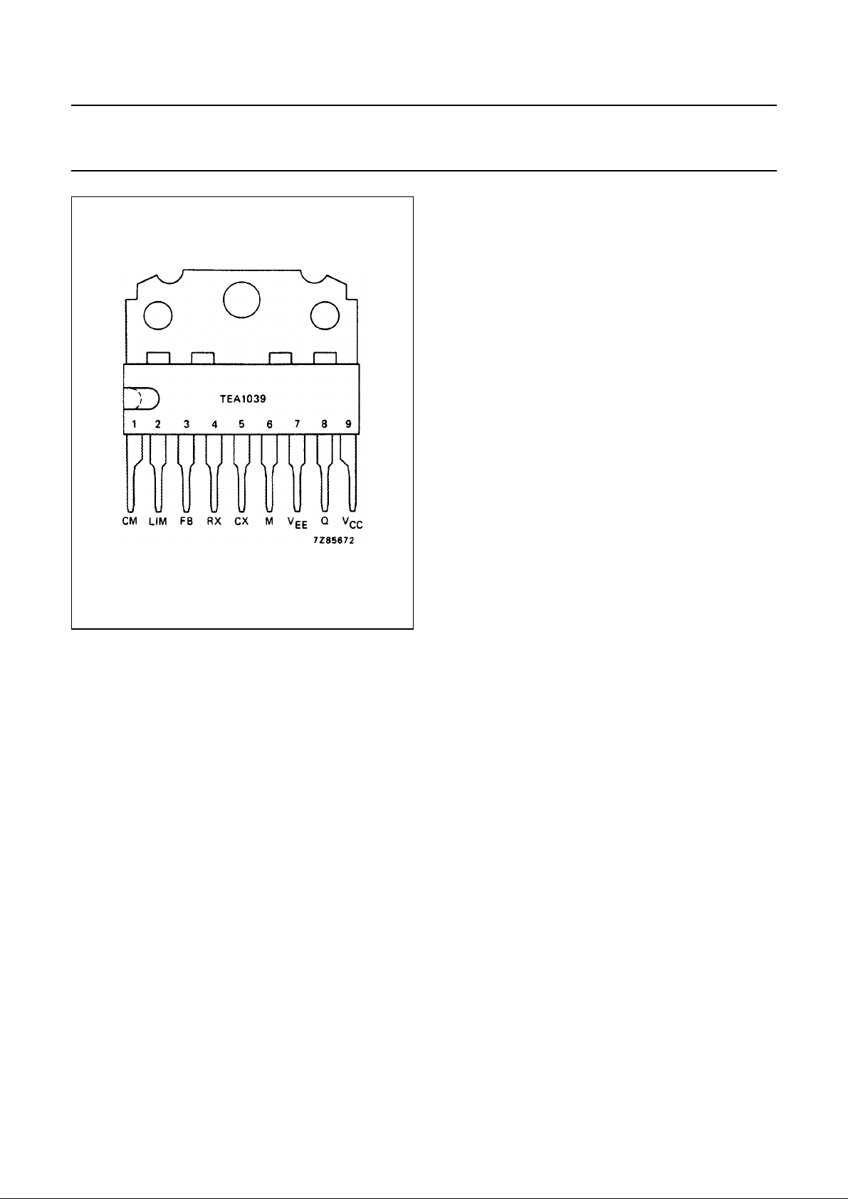
PACKAGE OUTLINE
9-lead SIL; plastic (SOT-110B); SOT110-1; 1996 November 18.
CC
o
OL
CC
amb
nom. 14 V
max. 13 mA
1 Hz to 100 kHz
max. 1 A
−25 to +125 °C
August 1982 2
Philips Semiconductors Product specification
Control circuit for switched-mode power
supply
TEA1039
August 1982 3
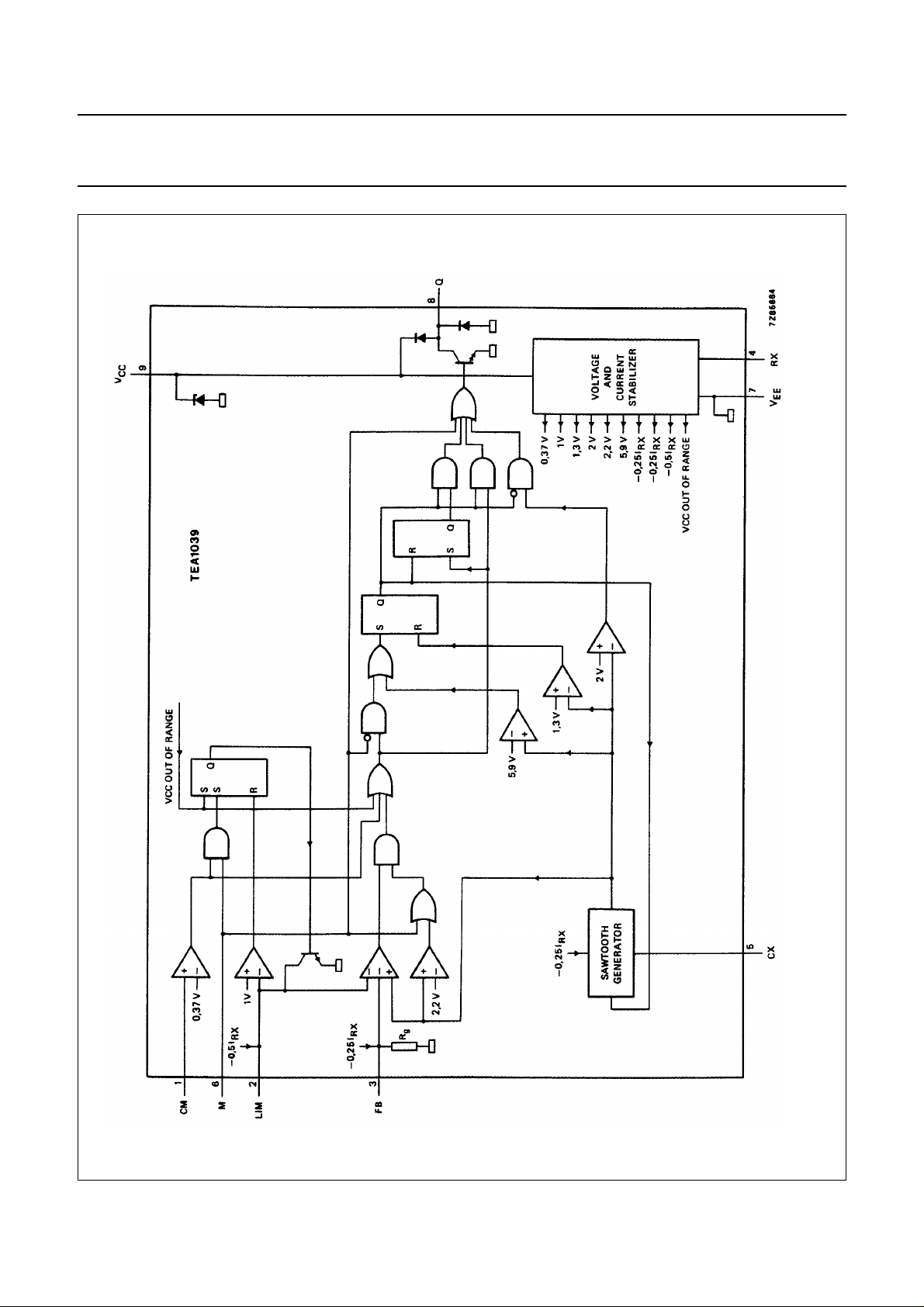
Fig.1 Block diagram.
Philips Semiconductors Product specification
Control circuit for switched-mode power supply TEA1039
PINNING
1 CM overcurrent protection input
2 LIM limit setting input
3 FB feedback input
4 RX external resistor connection
5 CX external capacitor connection
6 M mode input
7V
8 Q output
9V
common
EE
positive supply connection
CC
Fig.2 Pinning diagram.
FUNCTIONAL DESCRIPTION
The TEA1039 produces pulses to drive the transistor in a
switched-mode power supply. These pulses may be varied
either in frequency (frequency regulation mode) or in width
(duty factor regulation mode).
The usual arrangement is such that the transistor in the
SMPS is ON when the output of the TEA1039 is HIGH, i.e.
when the open-collector output transistor is OFF. The duty
factor of the SMPS is the time that the output of the
TEA1039 is HIGH divided by the pulse repetition time.
Supply V
CC
(pin 9)
The circuit is usually supplied from the SMPS that it
regulates. It may be supplied either from its primary d.c.
voltage or from its output voltage. In the latter case an
auxiliary starting supply is necessary.
The circuit has an internal V
out-of-range protection. In
CC
the frequency regulation mode the oscillator is stopped; in
the duty factor regulation mode the duty factor is made
zero. When the supply voltage returns within its range, the
circuit is started with the slow-start procedure.
When the circuit is supplied from the SMPS itself, the
out-of-range protection also provides an effective
protection against any interruption in the feedback loop.
Mode input M (pin 6) The circuit works in the frequency regulation mode when
the mode input M is connected to ground (V
, pin 7). In
EE
this mode the circuit produces output pulses of a constant
width but with a variable pulse repetition time.
The circuit works in the duty factor regulation mode when
the mode input M is left open. In this mode the circuit
produces output pulses with a variable width but with a
constant pulse repetition time.
Oscillator resistor and capacitor connections RX and CX (pins 4 and 5)
The output pulse repetition frequency is set by an oscillator
whose frequency is determined by an external capacitor
C5 connected between the CX connection (pin 5) and
ground (V
, pin 7), and an external resistor R4connected
EE
between the RX connection (pin 4) and ground. The
capacitor C5 is charged by an internal current source,
whose current level is determined by the resistor R4. In the
frequency regulation mode these two external
August 1982 4

Philips Semiconductors Product specification
Control circuit for switched-mode power supply TEA1039
components determine the minimum frequency; in the
duty factor regulation mode they determine the working
frequency (see Fig.4). The output pulse repetition
frequency varies less than 1% with the supply voltage over
the supply voltage range.
In the frequency regulation mode the output is LOW from
the start of the cycle until the voltage on the capacitor
reaches 2 V. The capacitor is further charged until its
voltage reaches the voltage on either the feedback input
FB or the limit setting input LIM, provided it has exceeded
2,2 V. As soon as the capacitor voltage reaches 5,9 V the
capacitor is discharged rapidly to 1,3 V and a new cycle is
initiated (see Figs 5 and 6).
For voltages on the FB and LIM inputs lower than 2,2 V,
the capacitor is charged until this voltage is reached; this
sets an internal maximum frequency limit.
In the duty factor regulation mode the capacitor is charged
from 1,3 V to 5,9 V and discharged again at a constant
rate. The output is HIGH until the voltage on the capacitor
exceeds the voltage on the feedback input FB; it becomes
HIGH again after discharge of the capacitor (see Figs 7
and 8). An internal maximum limit is set to the duty factor
of the SMPS by the discharging time of the capacitor.
Feedback input FB (pin 3) The feedback input compares the input current with an
internal current source whose current level is set by the
external resistor R4. In the frequency regulation mode, the
higher the voltage on the FB input, the longer the external
capacitor C5 is charged, and the lower the frequency will
be. In the duty factor regulation mode external capacitor
C5 is charged and discharged at a constant rate, the
voltage on the FB input now determines the moment that
the output will become LOW. The higher the voltage on the
FB input, the longer the output remains HIGH, and the
higher the duty factor of the SMPS.
Limit setting input LIM (pin 2) In the frequency regulation mode this input sets the
minimum frequency, in the duty factor regulation mode it
sets the maximum duty factor of the SMPS. The limit is set
by an external resistor R2 connected from the LIM input to
ground (pin 7) and by an internal current source, whose
current level is determined by external resistor R4.
A slow-start procedure is obtained by connecting a
capacitor between the LIM input and ground. In the
frequency regulation mode the frequency slowly
decreases from f
factor regulation mode the duty factor slowly increases
from zero to the working duty factor.
Overcurrent protection input CM (pin 1) A voltage on the CM input exceeding 0,37 V causes an
immediate termination of the output pulse. In the duty
factor regulation mode the circuit starts again with the
slow-start procedure.
Output Q (pin 8) The output is an open-collector n-p-n transistor, only
capable of sinking current. It requires an external resistor
to drive a n-p-n transistor in the SMPS (see Figs 9 and 10).
The output is protected by two diodes, one to ground and
one to the supply.
At high output currents the dissipation in the output
transistor may necessitate a heatsink. See the power
derating curve (Fig.3).
to the working frequency. In the duty
max
August 1982 5
 Loading...