

Philips TEA1024T Datasheet

DATA SH EET
Product specification
Supersedes data of 1996 Sep 05
File under Integrated Circuits, IC03
1998 Mar 02
INTEGRATED CIRCUITS
TEA1204T
High efficiency DC/DC converter

1998 Mar 02 2
Philips Semiconductors Product specification
High efficiency DC/DC converter TEA1204T
FEATURES
• Fully integrated DC/DC converter circuit
• Up-or-down conversion, each in 2 different modes
• High efficiency (up to 96%) at high loads
• Output power up to 3.6 W (typ.) continuous, 8 W in GSM
burst mode
• Low quiescent power consumption
• Burst mode input for optimal dynamic response to
switching loads
• True current limit for LiIon battery compatibility
• Up to 100% duty cycle in down mode
• Shut-down function
• 8-pin SO package.
APPLICATIONS
• Cellular and cordless phones PDAs and others
• Supply voltage source for low-voltage chip sets
• Portable computers
• Battery backup supplies
• Cameras.
GENERAL DESCRIPTION
The TEA1204T is a fully integrated DC/DC converter
circuit using the minimum amount of external components.
It is intended to be used to supply electronic circuits with
supply voltages of 3.3, 3.6 or 5.0 V from 2, 3 or 4 NiCd cell
batteries or one LiIon battery at an output power level up
to 3.6 W (typ.) continuously, or 8 W in GSM TDMA (1 : 8)
burst mode. Efficient, compact and dynamic power
conversion is achieved using a novel, digitally controlled
Pulse Width and Frequency Modulation (PWFM) like
control concept, integrated low R
dsON
CMOS power
switches with low parasitic capacitances and synchronous
rectification.
ORDERING INFORMATION
TYPE NUMBER
PACKAGE
NAME DESCRIPTION VERSION
TEA1204T SO8 plastic small outline package; 8 leads; body width 3.9 mm SOT96-1
1998 Mar 02 3
Philips Semiconductors Product specification
High efficiency DC/DC converter TEA1204T
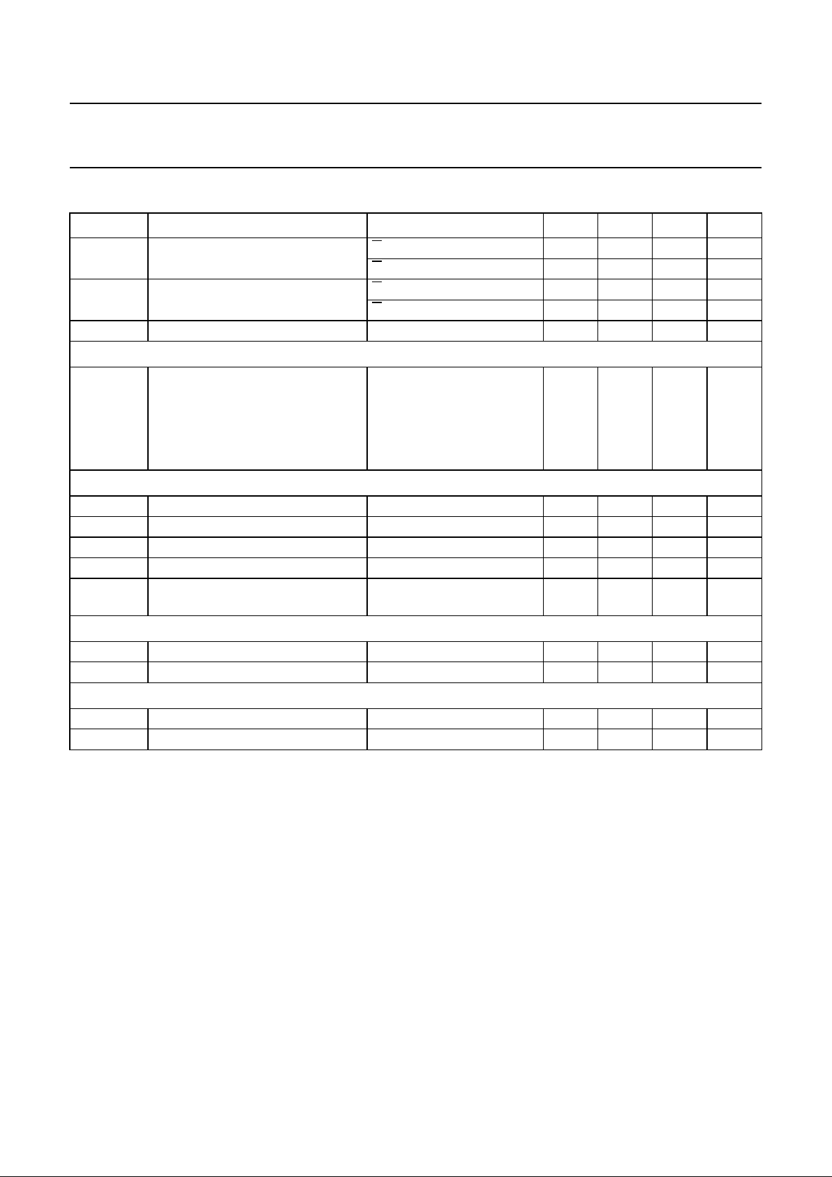
QUICK REFERENCE DATA
SYMBOL PARAMETER CONDITIONS MIN. TYP. MAX. UNIT
V
O(up)
output voltage in up mode U/D = LOW, VSEL = LOW 4.75 5.05 5.35 V
U/D = LOW; VSEL = HIGH 3.13 3.34 3.54 V
V
O(down)
output voltage in down mode U/D = HIGH; VSEL = LOW 3.42 3.64 3.85 V
U/D = HIGH; VSEL = HIGH 3.13 3.34 3.54 V
V
start
start-up voltage up mode 1.6 2.0 2.2 V
Efficiency
η efficiency
from 2.4 to 3.3 V 1 mA < I
L
<1.0A 839095%
from 3.6 to 5.0 V 1 mA < I
L
<1.0A 829094%
from 5.0 to 3.6 V 1 mA < I
L
<1.0A 809295%
from 5.0 to 3.3 V 1 mA < I
L
<1.0A 789094%
Current levels
I
q
quiescent current at pin 3 up mode 50 60 70 µA
I
SHDWN
shut-down current − 210µA
I
limN
current limit NFET up mode 2.38 2.80 3.20 A
I
limP
current limit PFET down mode 2.05 2.40 2.75 A
I
LX(max)
maximum continuous current at
pin 5
−−1.0 A
Power MOSFETS
R
dsON(N)
pin-to-pin resistance NFET 0.08 0.12 0.20 Ω
R
dsON(P)
pin-to-pin resistance PFET 0.10 0.16 0.25 Ω
Timing
f
sw
switching frequency 150 200 240 kHz
t
res
response time from standby to P
max
− 25 −µs
1998 Mar 02 4
Philips Semiconductors Product specification
High efficiency DC/DC converter TEA1204T
This text is here in white to force landscape pages to be rotated correctly when browsing through the pdf in the Acrobat reader.This text is here in
_white to force landscape pages to be rotated correctly when browsing through the pdf in the Acrobat reader.This text is here inThis text is here in
white to force landscape pages to be rotated correctly when browsing through the pdf in the Acrobat reader. white to force landscape pages to be ...
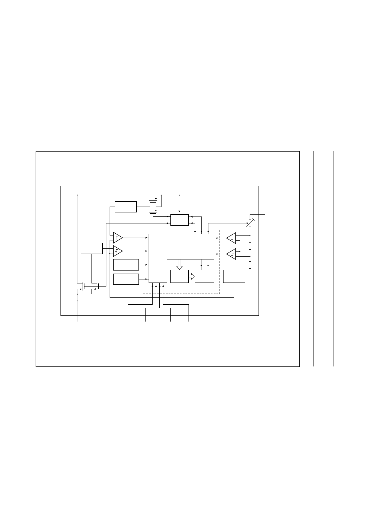
BLOCK DIAGRAM
a
ndbook, full pagewidth
MGK923
CONTROL LOGIC
AND
MODE GEARBOX
ROM
START-UP
CIRCUIT
I/V
CONVERTER
I/V
CONVERTER
TIME
COUNTER
BANDGAP
REFERENCE
20 MHz
OSCILLATOR
TEMPERATURE
PROTECTION
DIGITAL CONTROLLER
sense FET
P-type POWER FET
sense
FET
VSEL
GND
BURST SHDWNU/D
N-type
POWER
FET
LX
UPOUT/DNIN
SENSE
TEA1204T
16278
5
3
4
I
IimP
I
IimN
Fig.1 Block diagram.
1998 Mar 02 5
Philips Semiconductors Product specification
High efficiency DC/DC converter TEA1204T
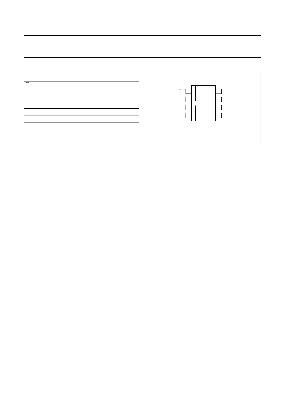
PINNING
SYMBOL PIN DESCRIPTION
U/D 1 conversion mode selection input
VSEL 2 output voltage selection input
UPOUT/DNIN 3 up mode; output voltage/
down mode; input voltage
SENSE 4 output voltage sense input
LX 5 inductor connection
GND 6 ground
BURST 7 burst mode trigger input
SHDWN 8 shut-down input
Fig.2 Pin configuration.
handbook, halfpage
MBH564
1
2
3
4
8
7
6
5
U/D SHDWN
VSEL BURST
UPOUT/DNIN GND
SENSE LX
TEA1204T
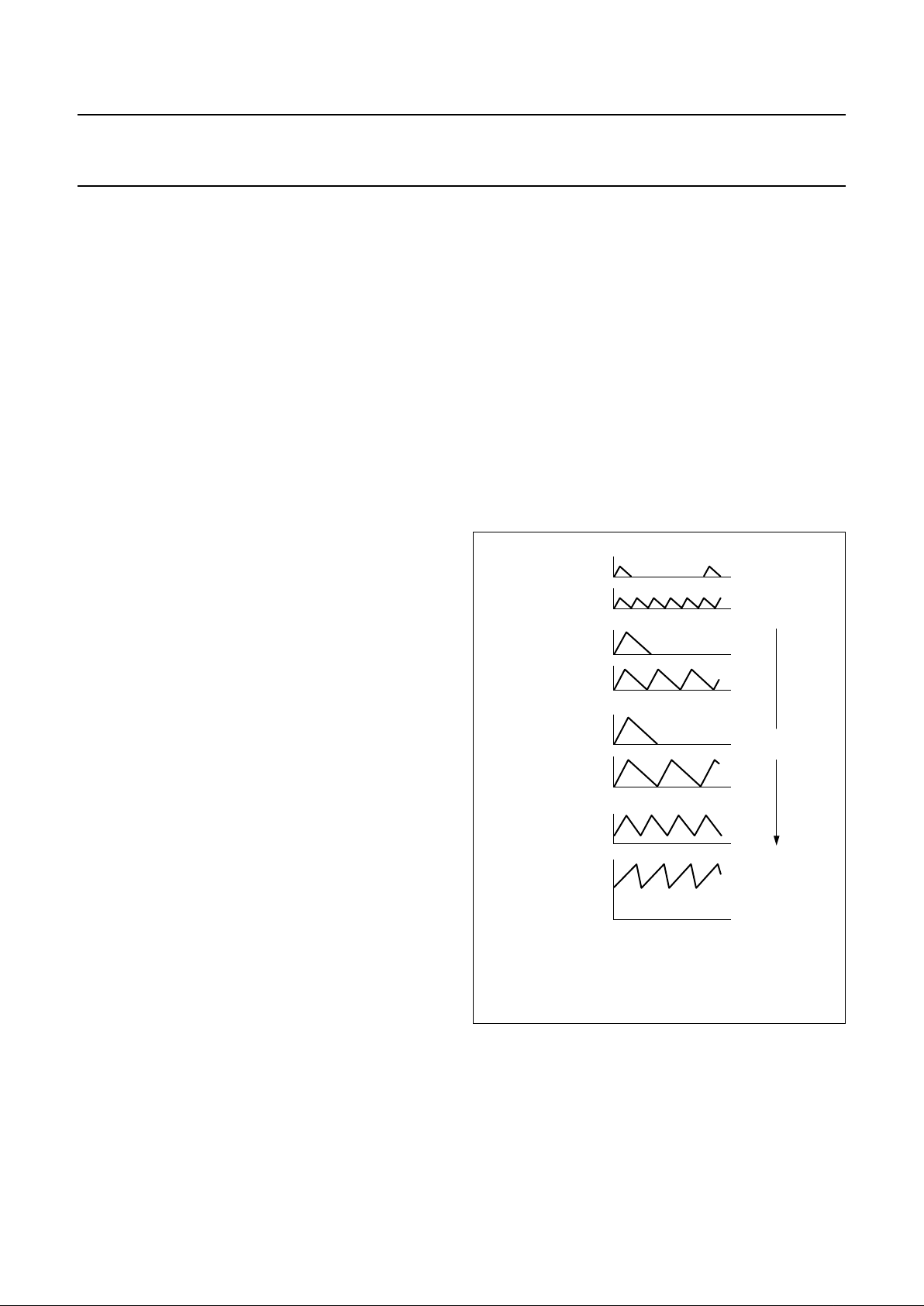
FUNCTIONAL DESCRIPTION
Control mechanism
The TEA1204T DC/DC converter is able to operate in
discontinuous or continuous conduction operation.
All switching actions are completely determined by a
digital control circuit which uses the output voltage level as
its control input. This novel digital approach enables the
use of a new pulse width and frequency modulation
scheme, which ensures optimum power efficiency over the
complete range of operation of the converter. The scheme
works as follows. At low output power, a very small current
pulse is generated in the inductor, and the pulse rate
varies with a varying load. When the output voltage drops
below a specific limit, which indicates that the converter’s
current capability is not sufficient, the digital controller
switches to the next state of operation. The peak current in
the inductor is made higher, and the pulse rate can again
vary with a varying load. A third operational state is
available for even higher currents.
When high output power is requested, the device starts
operating in continuous conduction mode. This results in
minimum AC currents in the circuit components and hence
optimum efficiency, cost, and EMC. In this mode, the
output voltage is allowed to vary between two predefined
voltage levels. As long as the output voltage stays within
this so-called window, switching continues in a fixed
pattern. When the output voltage reaches one of the
window borders, the digital controller immediately reacts
by adjusting the pulse width and inserting a current step in
such a way that the output voltage stays within the window
with higher or lower current capability. This approach
enables very fast reaction to load variations. Figure 3
shows the various coil current waveforms for low and high
current capability in each power conversion mode.
Figure 4 shows the converter’s response to a sudden load
increase. The upper trace shows the output voltage.
The ripple on top of the DC level is a result of the current
in the output capacitor, which changes in sign twice per
cycle, times the capacitor’s internal Equivalent Series
Resistance (ESR). After each ramp-down of the inductor
current, i.e. when the ESR effect increases the output
voltage, the converter determines what to do in the next
cycle. As soon as more load current is taken from the
output the output voltage starts to decay. When the output
voltage becomes lower than the low limit of the window, a
corrective action is taken by a ramp-up of the inductor
current during a much longer time. As a result, the DC
current level is increased and normal continuous
conduction mode can continue. The output voltage
(including ESR effect) is again within the predefined
window.
Figure 5 depicts the spread of the output voltage window.
The absolute value is most dependent on spread, while the
actual window size is not affected. For one specific device,
the output voltage will not vary more than 4%.
Start-up
A possible deadlock situation in boost configuration can
occur after a sequence of disconnecting and reconnecting
the input voltage source. If, after disconnection of the input
source, the output voltage falls below 2.0 V, the device
may not restart properly after reconnection of the input
source, and may take continuous current from the input.
An external circuit to prevent the deadlock situation is
shown in Chapter “Application information”.
1998 Mar 02 6
Philips Semiconductors Product specification
High efficiency DC/DC converter TEA1204T
Burst mode trigger input
For burst-mode applications, in which the required output
power periodically changes between two different power
levels, the burst mode trigger feature gains optimal
dynamic response. A digital signal indicating the load
change must be connected to the burst pin. Polarity of the
burst signal is arbitrary. When not used, the burst pin must
be tied to pin 3 or pin 6.
Shut-down
When the shut-down pin is made HIGH, the converter
disables both switches and power consumption is reduced
to a few µA.
Power switches
The power switches in the IC are one N-type and one
P-type MOSFET, having a typical pin-to-pin resistance of
0.12 Ω and 0.16 Ω respectively. The maximum average
current in the switches is 1.0 A.
Temperature protection
At too high device temperature (typical 165 °C), the
converter stops operating. It resumes operation when the
device temperature falls below 165 °C again. As a result,
low-frequent cycling between on and off state will occur.
It should be noted that in the event of device temperatures
around the cut-off limit, the application differs strongly from
maximum specifications.
Current limiters
If the current in one of the power switches exceeds its limit,
current ramping is stopped immediately, and the next
switching phase is entered. Current limitation is required to
enable optimal use of energy in Lithium-Ion batteries, and
to keep power conversion efficient during temporary high
loads. Furthermore, current limitation protects the IC
against overload conditions, inductor saturation, etc.
Behaviour at input voltage exceeding the specified
range
In general, an input voltage exceeding the specified range
is not recommended since instability may occur. There are
two exceptions:
• Upconversion: at an input voltage equal to or higher than
the target output voltage, but up to 6 V, the converter will
stop switching and the external schottky diode will take
over, resulting in V
o
equalling Vi minus the diode voltage
drop.
• Downconversion: when the input voltage is equal to or
lower than the target output voltage, but higher than
2.6 V, the P-type FET will stay conducting resulting in V
o
being equal to Vi minus some resistive voltage drop.
The current limit function remains active.
Fig.3 Coil current waveforms in the various power
modes.
handbook, halfpage
time
low power
mode
medium power
mode 1
medium power
mode 2
low DC current
high DC current
increasing
load
MGK924
 Loading...