

Philips TEA0679T Datasheet
INTEGRATED CIRCUITS
DATA SH EET
TEA0679T
2
I
C-bus controlled dual Dolby*
B-type noise reduction circuit for
playback applications
Product specification
Supersedes data of 1998 Jun 24
File under Integrated Circuits, IC01
1998 Nov 12
Philips Semiconductors Product specification
I2C-bus controlled dual Dolby* B-type noise
reduction circuit for playback applications
FEATURES
• Dual Noise Reduction (NR) channels
• Head preamplifiers
• Reverse head switching
• Automatic Music Search (AMS)
• Blank skip
• Mute position
• Equalization with electronically switched time constants
• Switch functions and level adjustment controlled via
I2C-bus
• Optional switch inputs TTL compatible
• Dolby reference level = 387.5 mV
• Contained in a 32-pin small outline package
• Improved EMC behaviour.
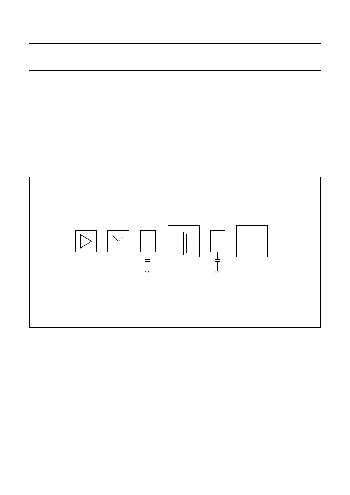
GENERAL DESCRIPTION
The TEA0679T is a bipolar integrated circuit that provides
two channels of Dolby B noise reduction for playback
applications in car radios. It includes head and
equalization amplifiers with electronically switchable time
constants. The device also includes electronically
switchable inputs for tape drivers with reverse heads.
This device detects pauses of music in the Automatic
Music Search (AMS) scan mode (for applications with an
intelligent controlled tape driver) or AMS latch mode (for
applications with a simple controlled tape driver).
For both modes the delay time can be fixed by using an
external resistor. In the blank skip mode the IC can detect
pauses of music during playback and allows a
microcontroller to react on this situation.
The equalization amplifier gain adjustment, the output
offset adjustment and all switching functions are I
controlled. Head switching and equalization time constant
switching can be controlled via separate pins (optional).
The device operates with power supplies from 7.6 to 12 V.
The output overload level increases with increases in
supply voltage.
Current drain varies with the following variables:
• Supply voltage
• Noise reduction on/off
• AMS on/off.
Because of this current drain variation it is advisable to use
a regulated power supply or a supply with a long time
constant.
TEA0679T
2
C-bus
QUICK REFERENCE DATA
SYMBOL PARAMETER MIN. TYP. MAX. UNIT
V
CC
I
CC
SN+
-------------N
ORDERING INFORMATION
TYPE
NUMBER
TEA0679T SO32 plastic small outline package; 32 leads; body width 7.5 mm SOT287-1
Remark Dolby*: Available only to licensees of Dolby Laboratories Licensing Corporation, San Francisco, CA94111,
USA, from whom licensing and application information must be obtained. Dolby is a registered trade-mark of Dolby
Laboratories Licensing Corporation.
1998 Nov 12 2
supply voltage 7.6 − 12 V
supply current − 35 40 mA
signal plus noise-to-noise ratio 78 84 − dB
PACKAGE
NAME DESCRIPTION VERSION
This text is here in white to force landscape pages to be rotated correctly when browsing through the pdf in the Acrobat reader.This text is here in
_white to force landscape pages to be rotated correctly when browsing through the pdf in the Acrobat reader.This text is here inThis text is here in
white to force landscape pages to be rotated correctly when browsing through the pdf in the Acrobat reader. white to force landscape pages to be ...
1998 Nov 12 3
handbook, full pagewidth
BLOCK DIAGRAM
reduction circuit for playback applications
I
2
C-bus controlled dual Dolby* B-type noise
Philips Semiconductors Product specification
BEN
32
1
MAD
SDA
31
I2C-BUS
2
BSC
220 nF
output B
SCL
3
TD
R
t
(ref)
output A
4
BTC
47 nF
EQS
(opt)
10 µF
282930
EQS
10 µF
OUTBDGND AMS
27
65
OUTA
330 nF
(±10%)
270 kΩ
(±10%)
INTB
MUTE
7
INTA
270 kΩ
(±10%)
330 nF
(±10%) (±5%)
100 nF
(±10%)
180 kΩ
(±10%)
CONTRB
2526
DOLBY B
LATCH
AND
RISE TIME
DELAY
TIME
DOLBY B
8
CONTRA
180 kΩ
(±10%)
100 nF
(±10%)
15 nF
(±5%)
HPB
24
AMS
PROCESSOR
LEVEL
DETECTOR
9
(±5%)
4.7 nF
(±5%)
SCB
23
10
SCAHPA
4.7 nF15 nF
BLANK
SKIP
24 kΩ
(±2%)
24 kΩ
(±2%)
390 kΩ
EQB
22
LOGIC
11
EQA
390 kΩ
8.2
nF
5.6
kΩ
5.6
kΩ
8.2
nF
EQ
AMP
EQ
AMP
EQFB
21
12
EQFA
2.7 kΩ
2.7 kΩ
AGND
20
13
V
CC
10 µF
POWER
SUPPLY
10 µF
PRE
AMP
PRE
AMP
470
pF
INB1
INA1
470
pF
HS
(opt)
HS
19
18
TEA0679T
15
14
V
470
pF
INB2
17
16
INA2
ref
100
µF
470
pF
TEA0679T
Fig.1 Block and application diagram.
MHB117
Philips Semiconductors Product specification
I2C-bus controlled dual Dolby* B-type noise
reduction circuit for playback applications
PINNING
SYMBOL PIN DESCRIPTION
MAD 1 programmable address bit
BSC 2 blank skip reference capacitance
TD 3 delay time constant
BTC 4 blank skip integration capacitance
EQS 5 equalization switch input (optional)
OUTA 6 output channel A
INTA 7 integrating filter channel A
CONTRA 8 control voltage channel A
HPA 9 high-pass filter channel A
SCA 10 side chain channel A
EQA 11 equalizing output channel A
EQFA 12 equalizing input channel A
V
CC
INA1 14 input channel A1 (forward or reverse)
V
ref
INA2 16 input channel A2 (reverse or forward)
INB2 17 input channel B2 (reverse or forward)
HS 18 head switch input (optional)
INB1 19 input channel B1 (forward or reverse)
AGND 20 analog ground
EQFB 21 equalizing input channel B
EQB 22 equalizing output channel B
SCB 23 side chain channel B
HPB 24 high-pass filter channel B
CONTRB 25 control voltage channel B
INTB 26 integrating filter channel B
OUTB 27 output channel B
AMS
DGND 29 digital ground
SCL 30 serial clock input
SDA 31 serial data input/output
BEN 32 bus enable
13 supply voltage
15 reference voltage
Automatic Music Search (AMS)
28
output
handbook, halfpage
MAD
1
BSC
2
TD
3
BTC
4
EQS
5
OUTA
6
INTA
7
CONTRA
HPA
SCA
EQA
EQFA
V
CC
INA1
V
INA2
ref
8
TEA0679T
9
10
11
12
13
14
15
16
Fig.2 Pin configuration.
MHB118
TEA0679T
BEN
32
SDA
31
SCL
30
DGND
29
AMS
28
OUTB
27
INTB
26
CONTRB
25
HPB
24
SCB
23
EQB
22
EQFB
21
AGND
20
INB1
19
HS
18
INB2
17
1998 Nov 12 4

Philips Semiconductors Product specification
I2C-bus controlled dual Dolby* B-type noise
reduction circuit for playback applications
FUNCTIONAL DESCRIPTION
The following functions can be controlled via the I2C-bus:
• Equalization time constant switching
• Head switching
• Automatic Music Search (AMS) modes and blank skip
• Noise Reduction (NR) on/off switching
• Mute switching
• Equalization amplifier gain adjustment
• Output offset adjustment.
Dolby B noise reduction only operates correctly if the 0 dB
Dolby level is adjusted at 387.5 mV. The gain adjustment
can also be used to change the AMS level detector
threshold. The IC is able to generate an internal power-on
reset to guarantee a proper start-up behaviour.
Two of the above functions can be controlled via separate
pins (optional), if required.
Head switching is achieved when pin HS is connected to a
LOW level (input IN2 active) or connected to a HIGH level
(input IN1 active).
Equalization time constant switching (70 or 120 µs) is
achieved when pin EQS is connected to a LOW level
(70 µs) or connected to a HIGH level (120 µs).
2
C-bus control is used the respective external function
If I
control pin has to be left open-circuit. When open-circuit
the current state of the function can be observed at these
pins.
Automatic Music Search (AMS) modes and blank skip
If AMS is active (search mode bits SMOD1 = 1 and
SMOD0 = 0 or 1) the NR function is internally switched off
and the equalization time constant is internally forced to
70 µs. The signals of both channels are full-wave rectified
and then added. This means that even if one channel
appears inverted to the other channel the normal AMS
function is ensured.
It is possible to choose between the AMS scan and the
AMS latch mode via the I
internal flip-flop the switching from one mode to the other
must be done via the AMS off state. This guarantees an
appropriate flip-flop reset:
• Start from the initial AMS off state (SMOD1 = 0 and
SMOD0 = 0 or 1)
• Enable the desired AMS operation mode: AMS latch
mode (SMOD1 = 1 and SMOD0 = 0) or AMS scan mode
(SMOD1 = 1 and SMOD0 = 1).
2
C-bus. Due to the usage of an
TEA0679T
For further information on music search see Figs 4 to 8.
If blank skip is active (SMOD1 = 0 and SMOD0 = 1)
periods of music can be detected in the playback mode
using the AMS pin as the detector output. It is possible to
defeat this function via the I
SMOD0 = 0). For further information on blank skip
see Figs 9 and 10.
Offset adjustment procedure
The offset adjustment is performed using two bits in the
2
C-bus write byte 0. The offset monitor bit OMOR enables
I
the AMS output to indicate whether the selected offset
value is positive or negative. The channel select bit OFCH
selects the channel (A or B) which is currently monitored
by the output at pin AMS. The monitoring needs a few
microseconds until the output result is valid. A complete
offset adjustment is performed in the following way:
• Adjust the output to Dolby level using the I
controlled equalization gain adjustment
• Enable the offset monitor and select the channel to be
monitored by transmitting the bits OMOR = 1 and OFCH
(0 = Channel A, 1 = Channel B) to the IC
• If the monitor output (pin AMS) is LOW send the next
offset value OFFCHA or OFFCHB one offset step below
the last valid value. If the monitor output (pin AMS) is
HIGH send the next offset value OFFCHA or OFFCHB
one offset step above the last valid value
• Repeat the last two steps until the monitor output
changes its polarity
• If necessary store the transmitted digital offset value for
the selected channel.
The start value is either set by the power-on reset or the
last I2C-bus transmission. The offset adjustment can be
performed during the power-on reset condition and also
each time the tape driver is not active. A complete digital
offset data set consists of four values: one for each head
(head 1 and head 2) in each channel. After an offset value
transmission the IC stores one value for channel A and
one value for channel B. If a head switch is performed
these values have to be updated via the I2C-bus for the
alternative head.
2
C-bus (SMOD1 = 0 and
2
C-bus
1998 Nov 12 5
Philips Semiconductors Product specification
I2C-bus controlled dual Dolby* B-type noise
TEA0679T
reduction circuit for playback applications
I2C-bus operation mode
The IC is capable of operating with I2C-bus systems that provide either 5 V or digital supply voltage related logic levels
below 5 V. This is achieved using the bus enable (pin 32) with different input voltages. An open pin or input voltages
above 5 V enable 5 V related I2C-bus logic levels. If input voltages between 3 and 5 V are used the IC operates with
I2C-bus logic levels related to these input voltages. To disable the I2C-bus receiver it is necessary to use pin voltages
below the specified LOW level.
LIMITING VALUES
In accordance with the Absolute Maximum Rating System (IEC 134).
SYMBOL PARAMETER CONDITIONS MIN. MAX. UNIT
V
CC
V
i
V
i(n1)
V
i(n2)
V
i(stb)
t
sc
T
stg
T
amb
V
es
supply voltage 0 14 V
input voltage (pins 1 to 32) except pin 5 (EQS),
pin 15 (V
(SDA) to V
), pin 18 (HS), pin 30 (SCL) and pin 31
ref
CC
−0.3 V
CC
V
input voltage at pin 30 (SCL) and pin 31 (SDA) −0.3 +12 V
input voltage at pin 5 (EQS) and pin 18 (HS) −0.3 +6.5 V
standby input voltage at pin 1 (MAD), pin 32 (BEN),
note 1 −0.3 +6.5 V
pin 5 (EQS) and pin 18 (HS)
pin 15 (V
) to VCC short-circuiting duration − 5s
ref
storage temperature −55 +150 °C
operating ambient temperature −40 +85 °C
electrostatic handling voltage for all pins note 2 −2+2kV
note 3 −500 +500 V
Notes
1. The TEA0679T allows a HIGH level at switching pins without voltage (V
= 0; standby mode). This means a
CC
maximum input voltage of 6.5 V for the switching pins.
2. Human body model (1.5 kΩ; 100 pF).
3. Machine model (0 Ω; 200 pF).
THERMAL CHARACTERISTICS
SYMBOL PARAMETER CONDITIONS VALUE UNIT
R
th(j-a)
thermal resistance from junction to ambient in free air 62 K/W
1998 Nov 12 6

Philips Semiconductors Product specification
I2C-bus controlled dual Dolby* B-type noise
TEA0679T
reduction circuit for playback applications
CHARACTERISTICS
V
= 10 V; f = 20 Hz to 20 kHz; T
CC
(TP) pin OUTA or OUTB; see Fig.1; NR on/AMS off; EQ switch in the 70 µs position; unless otherwise specified.
SYMBOL PARAMETER CONDITIONS MIN. TYP. MAX. UNIT
V
CC
I
CC
α
m
supply voltage 7.6 10 12 V
supply current − 35 40 mA
channel matching f = 1 kHz; Vo= 0 dB; NR off −0.5 −+0.5 dB
THD total harmonic distortion
(2nd and 3rd harmonic)
H
R
SN+
-------------N
headroom at output VCC= 7.6 V; THD = 1%;
signal plus noise-to-noise ratio internal gain 40 dB, linear;
PSRR power supply ripple rejection V
V
o
output voltage frequency
response; referenced to TP
α
cs
α
ct
channel separation Vo= 10 dB; f = 1 kHz;
crosstalk between active and
inactive input
R
L
G
v
V
i(offset)(DC)
I
i(bias)
R
EQ
R
i
G
v(ol)
V
− V
ref
load resistance at output AC-coupled; f = 1 kHz;
voltage gain of preamplifier pin INA1/INA2 to pin EQFA;
DC input offset voltage − 2 − mV
input bias current − 0.1 0.4 µA
internal equalization resistor pin EQA/EQB to EQ amplifier
input resistance of head inputs 60 100 − kΩ
open-loop gain pin INA1 or INA2 to pin EQA;
DC output offset voltage at
OUT
pins OUTA and OUTB after
adjustment
=25°C; all levels are referenced to Vo= 387.5 mV (RMS) (0 dB) at test point
amb
f = 1 kHz; V
f = 10 kHz; V
=0dB − 0.08 0.15 %
o
=10dB − 0.15 0.3 %
o
12 −−dB
f = 1 kHz
78 84 − dB
CCIR/ARM weighted;
decode mode; see Fig.41
= 0.25 V; f = 1 kHz;
i(rms)
52 57 − dB
see Fig.38
encode mode; see Fig.41
−25 dB; f = 0.2 kHz −25.9 −24.4 −22.9 dB
0 dB; f = 1 kHz −1.5 0 +1.5 dB
−25 dB; f = 1 kHz −20.8 −19.3 −17.8 dB
−25 dB; f = 5 kHz −21.1 −19.6 −18.1 dB
−35 dB; f = 10 kHz −27.4 −25.9 −24.4 dB
57 63 − dB
see Fig.39
f = 1 kHz; Vo= 10 dB; NR off;
70 77 − dB
see Fig.39
10 −−kΩ
Vo= 12 dB; THD = 1%
29 30 31 dB
pin INB1/INB2 to pin EQFB;
f = 1 kHz
4.7 5.8 6.9 kΩ
A/B output
pin INB1 or INB2 to pin EQB;
additional gain=0dB
f = 10 kHz 80 86 − dB
f = 400 Hz 104 110 − dB
NR off; pins INA1, INA2, INB1
and INB2 connected to V
ref
−20 −+20 mV
1998 Nov 12 7
Philips Semiconductors Product specification
I2C-bus controlled dual Dolby* B-type noise
TEA0679T
reduction circuit for playback applications
SYMBOL PARAMETER CONDITIONS MIN. TYP. MAX. UNIT
I
O
Z
o
V
no(rms)
V
TD
V
offset(DC)
V
offset(AD)
Level adjustment
G
CR
G
step
G
E
DC output current pins OUTA and OUTB
−2 −−mA
connected to ground
pins OUTA and OUTB
connected to V
CC
0.3 −−mA
output impedance − 80 100 Ω
equivalent input noise voltage
(RMS value)
AMS timing (DC level) resistor Rt connected to pin TD VCC− 3 − V
DC offset voltage at pins OUTA
NR off; unweighted;
f = 20 Hz to 20 kHz;
R
f = 900 MHz; V
source
=0Ω
i(rms)
− 0.7 1.4 µV
CC
V
=6V − 40 − mV
and OUTB
overall offset voltage between
−0.4 − +0.4 V
AGND (pin 20) and DGND
(pin 29)
gain control range note 1 24.2 25.2 26.2 dB
step size − 0.4 − dB
step error between any
−−0.4 dB
adjacent step
Switching thresholds
O
PTIONAL EQUALIZATION TIME CONSTANT SWITCH (pin EQS)
V
IL
V
OL
V
IH
V
OH
LOW-level input voltage 70 µs; IL≥−200 µA −0.3 − +0.8 V
LOW-level output voltage 70 µs; IL≤ 1mA −−0.4 V
HIGH-level input voltage 120 µs2−−V
HIGH-level output voltage 120 µs; IL≥−50 µA 2.8 − 3.3 V
OPTIONAL HEAD SWITCH (pin HS)
V
IL
V
OL
V
IH
V
OH
LOW-level input voltage INPUT 2 on; IL≥−150 µA −0.3 − +0.8 V
LOW-level output voltage INPUT 2 on; IL≤ 10 µA −−0.4 V
HIGH-level input voltage INPUT 1 on 2 −−V
HIGH-level output voltage INPUT 1 on; IL≥−50 µA 2.8 − 3.3 V
Search modes
B
LANK SKIP
BS
th(M-P)
t
sw(P-M)
dynamic level threshold blank skip mode; f = 10 kHz −30 −27 −24 dB
switching time pause-to-music blank skip mode; f = 10 kHz;
signal on channel A and B;
note 2
blank skip mode; f = 10 kHz;
signal on one channel; note 2
t
sw(M-P)
switching time music-to-pause blank skip mode; f = 10 kHz;
note 2
2.1 4.15 6.3 ms
4.1 8.3 12.5 ms
10 19 30 ms
1998 Nov 12 8
Philips Semiconductors Product specification
I2C-bus controlled dual Dolby* B-type noise
TEA0679T
reduction circuit for playback applications
SYMBOL PARAMETER CONDITIONS MIN. TYP. MAX. UNIT
UTOMATIC MUSIC SEARCH (AMS)
A
t
W(min)(r)
AMS
(P-M)
AMS
(M-P)
OUTPUT (pin AMS)
V
OH
V
OL
Digital part (pins MAD and BEN)
V
IH
V
IL
I
IH
I
IL
Digital part (pins SDA and SCL); note 4
V
IH
V
IL
I
IH
I
IL
V
OL
Notes
1. For Dolby NR level adjust and AMS pause detection level setting.
2. All blank skip timing characteristics are based on the assumption that a signal level change from −33 to −21 dB
pause-to-music or −21 to −33 dB music-to-pause occurs in the specified channels.
3. The high speed of the tape (FF and REW) at the tape head during AMS mode causes a transformation of level and
frequency of the originally recorded signal. It means a boost of signal level of approximately 10 dB and more for
recorded frequencies from 500 Hz to 4 kHz. So the threshold level of−22 dB corresponds to signal levels in PlayBack
(PB) mode of approximately −32 dB. The AMS inputs for each channel are pins SCA and SCB. As the frequency
spectrum is transformed by a factor of approximately 10 to 30 due to the higher tape speed in FF and REW, the
high-pass filter (4.7 nF/24 kΩ) removes the effect of offset voltages but does not affect the music search function.
In the block and application diagram (see Fig.1) the frequency response of the system between tape heads input,
e.g. pins INA2 and INB2, to the AMS input pins SCA and SCB is constant over the whole frequency range (see
Fig.3).
4. These levels correspond to a gain setting of Dolby level at TP (for TP see Fig.41). The gain adjustment can be used
to change the threshold level during AMS operation.
5. The characteristics are in accordance with the I2C-bus specification. Information about the I2C-bus can be found in
the brochure
minimum pulse width rise time AMS scan mode 2 − 10 ms
AMS latch mode 130 − 170 ms
signal level at output for AMS
switching pause-to-music
AMS switching hysteresis
AMS mode; f = 10 kHz;
−23.7 −21 −18 dB
notes 3 and 4; see Fig.40
AMS mode; f = 10 kHz −0.7 −1 −1.3 dB
music-to-pause
HIGH-level output voltage IL≥−1 mA 2.8 − 3.3 V
LOW-level output voltage IL≤ 1mA −−0.4 V
HIGH-level input voltage 3 − V
CC
V
LOW-level input voltage −0.3 −+1.5 V
HIGH-level input current −10 −+10 µA
LOW-level input current −10 −+10 µA
HIGH-level input voltage BEN (pin 32) open-circuit 3 − V
5V≤V
3V≤V
≤ V
BEN
BEN
CC
< 5 V 0.7V
3 − V
− V
BEN
CC
CC
CC
V
V
V
LOW-level input voltage BEN (pin 32) open-circuit −0.3 −+1.5 V
5V≤V
3V≤V
≤ V
BEN
BEN
CC
<5V −0.3 − 0.3V
−0.3 −+1.5 V
BEN
V
HIGH-level input current VCC=0to12V −10 −+10 µA
LOW-level input current −10 −+10 µA
LOW-level output voltage SDA IL=3mA −−0.4 V
“The I2C-bus and how to use it”
(order number 9398 393 40011).
1998 Nov 12 9
Philips Semiconductors Product specification
I2C-bus controlled dual Dolby* B-type noise
TEA0679T
reduction circuit for playback applications
General note
It is recommended to switch off VCC with a gradient of 400 V/s at maximum to avoid plops on tape in the event of contact
between tape and tape head while switching off.
AMS delay time
Table 1 AMS delay time set by resistor R
RESISTOR VALUE R
(kΩ) DELAY TIME tdTYP. (ms) TOLERANCE (%)
t
68 23 20
150 42 15
180 48 15
220 56 15
270 65 10
330 76 10
470 98 10
560 112 10
680 126 10
820 142 10
1000 160 10
at pin TD
t
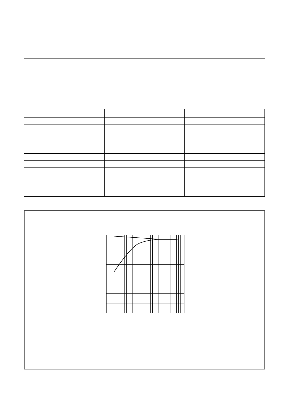
AMS threshold level
−20
handbook, halfpage
AMS
(P-M)
(dB)
−30
−40
−50
−60
(1) AMS threshold level for application circuit (see Fig.1).
(2) AMS threshold level for test circuit (see Fig.40).
MHB119
(1)
(2)
2
10
3
10
4
10
f (Hz)
5
10
Fig.3 AMS threshold level.
1998 Nov 12 10
Philips Semiconductors Product specification
I2C-bus controlled dual Dolby* B-type noise
reduction circuit for playback applications
Short description of music search
A system for music search consists mainly of a level and a
time detection circuit (see Fig.4). For adapting and
decoupling the input signal is amplified (A), then rectified
(B) and smoothed with a time constant (C). Thus the
voltage at (C) corresponds to the signal level and will be
compared to the predefined pause level at the first
comparator (D), the level detector. If the signal level
becomes smaller than the pause level, the level detector
changes its output signal. Due to the output level of the
level detector the capacitor of the second time constant (E)
will be charged, respectively discharged.
handbook, full pagewidth
INPUT
(A)
(B)
(C)
COMPARATOR 1 COMPARATOR 2
V
I
t
1
TEA0679T
If the pause level of the input signal remains for a certain
time period, the voltage at the capacitor reaches a certain
value, which corresponds to an equivalent time value.
The voltage at the capacitor will be compared to a
predefined time-equivalent voltage by the second
comparator (F), the time detector. If the pause level of the
input signal remains for this predefined time, the time
detector changes its output level to pause found status.
(D)
(E) (F)
V
t
t
2
OUTPUT
AMPLIFIER RECTIFIER
LEVEL DETECTOR TIME DETECTOR
MED624
Fig.4 Integrated music search function.
1998 Nov 12 11
Philips Semiconductors Product specification
I2C-bus controlled dual Dolby* B-type noise
reduction circuit for playback applications
Description of the principle timing diagram for AMS
scan mode without initial input signal (see Fig.5)
By activating the AMS scan mode the AMS output level
directly indicates whether the input level corresponds to a
pause level (V
At t0 the AMS scan mode is activated. Without a signal at
Vin, the following initial procedure runs until the AMS
output changes to a LOW level: due to no signal at Vin the
voltage at the level detector input VI (CONTRA) remains
below the level threshold and the second time constant will
be discharged (time detector input Vt). When Vt exceeds
the time threshold level, the time detector output changes
to LOW level. Now the initial procedure is completed.
If a signal burst appears at t3, the level detector input
voltage rises immediately and causes its output to charge
the second time constant, which supplies the input voltage
Vt for the time detector.
handbook, full pagewidth
= LOW) or not (V
AMSEQ
AMS on
V
in
t
r
AMSEQ
= HIGH).
t
d
t
f
TEA0679T
When V
time tr (at t4) the AMS output changes to HIGH. If the signal
burst ends at t5 the level detector input VI falls to its LOW
level. Discharging of the second time constant begins
when the level threshold is exceeded at t6. The circuit then
measures the delay time td, which is externally fixed by a
resistor and defines the length of a pause to be detected.
If no signal appears at Vin within the time interval td, the
time detector output switches the AMS output to a LOW
level at t7.
If a plop noise pulse appears at Vin (t8) with a pulse width
less than the rise time tr>tb, the plop noise will not be
detected as music. The AMS output remains LOW.
Similarly the system handles no music pulses tp: when
music appears at t11 with a small interruption at t13, this
interruption will not affect the AMS output for tp<td.
tb < t
exceeds the upper threshold level after the rise
t
r
tp < t
d
V
l
level threshold
V
ref
V
t
upper threshold
(hysteresis)
time threshold
V
AMSEQ
4.5 V
output signal
to microprocessor
t
0
tr= rise time; td= delay time; tb= burst time; tp= pause time; tf= fall time.
t3t
t5t
4
6
t
7
t8t9t
t
Vl: voltage at
level detector
input
pin 8 (CONTRA)
t
Vt: voltage at
time detector
input
pin 25 (CONTRB)
t
t
10
t11t
12t13t14
t
15
MHB120
Fig.5 AMS scan mode without initial input signal.
1998 Nov 12 12
 Loading...