

Page 1

INTEGRATED CIRCUITS
DATA SH EET
TDA9887
2
I
C-bus controlled multistandard
alignment-free IF-PLL demodulator
with FM radio
Product specification
Supersedes data of 2003 Oct 03
2004 Aug 25
Page 2

Philips Semiconductors Product specification
I2C-bus controlled multistandard alignment-free
IF-PLL demodulator with FM radio
CONTENTS
1 FEATURES
2 GENERAL DESCRIPTION
3 APPLICATIONS
4 ORDERING INFORMATION
5 QUICK REFERENCE DATA
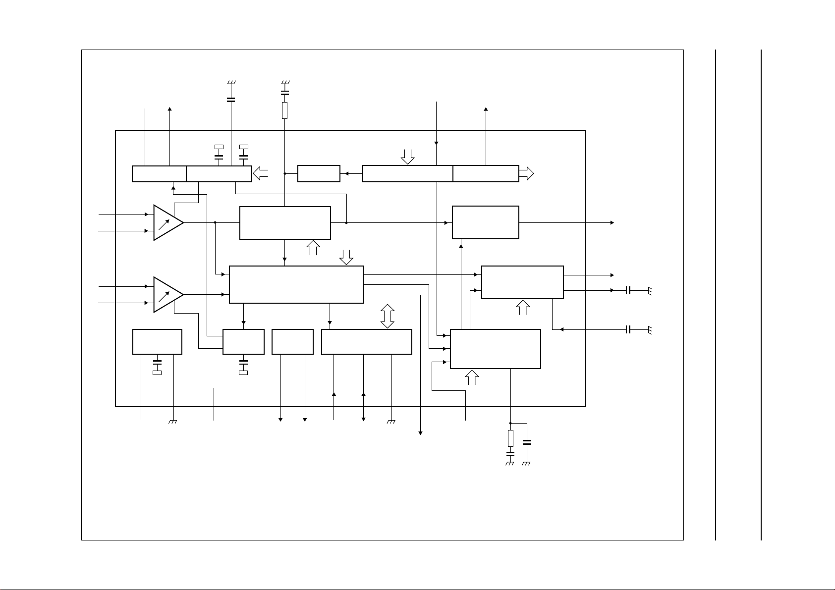
6 BLOCK DIAGRAM
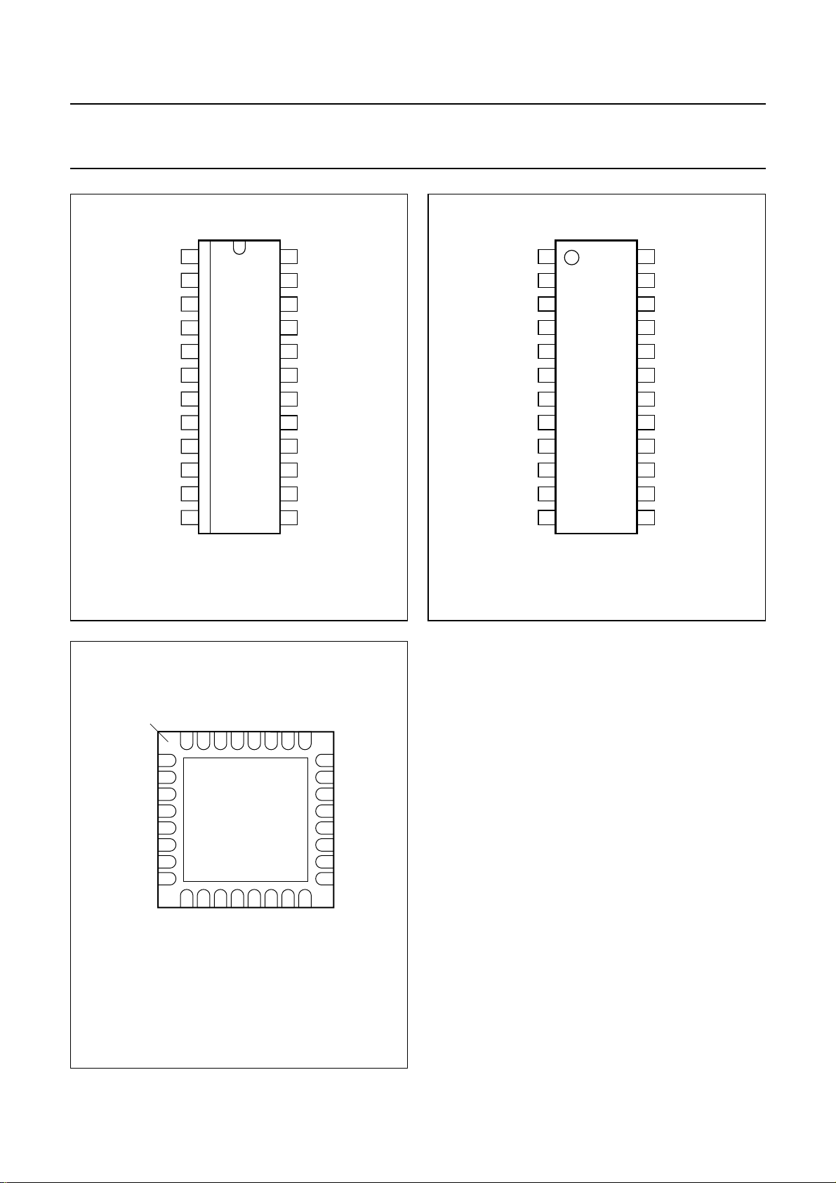
7 PINNING
8 FUNCTIONAL DESCRIPTION
8.1 VIF amplifier
8.2 Tuner AGC and VIF-AGC
8.3 VIF-AGC detector
8.4 FPLL detector
8.5 VCO and divider
8.6 AFC and digital acquisition help
8.7 Video demodulator and amplifier
8.8 Sound carrier trap
8.9 SIF amplifier
8.10 SIF-AGC detector
8.11 Single reference QSS mixer
8.12 AM demodulator
8.13 FM demodulator and acquisition help
8.14 Audio amplifier and mute time constant
8.15 Radio mode
8.16 Internal voltage stabilizer
8.17 I2C-bus transceiver and module address
9I
9.1 Read format
9.1.1 Slave address
9.1.2 Data byte
9.2 Write format
9.2.1 Subaddress
9.2.2 Data byte for switching mode
9.2.3 Data byte for adjust mode
9.2.4 Data byte for data mode
2
C-BUS CONTROL
10 LIMITING VALUES
11 THERMAL CHARACTERISTICS
12 CHARACTERISTICS
13 TEST AND APPLICATION INFORMATION
14 PACKAGE OUTLINES
15 SOLDERING
15.1 Introduction to soldering surface mount
packages
15.2 Reflow soldering
15.3 Wave soldering
15.4 Manual soldering
15.5 Suitability of surface mount IC packages for
wave and reflow soldering methods
16 DATA SHEET STATUS
17 DEFINITIONS
18 DISCLAIMERS
19 PURCHASE OF PHILIPS I2C COMPONENTS
TDA9887
2004 Aug 25 2
Page 3

Philips Semiconductors Product specification
I2C-bus controlled multistandard alignment-free
IF-PLL demodulator with FM radio
1 FEATURES
• 5 V supply voltage
• Gain controlled wide-band Vision Intermediate
Frequency (VIF) amplifier, AC-coupled
• Multistandard true synchronous demodulation with
active carrier regeneration: very linear demodulation,
good intermodulation figures, reduced harmonics, and
excellent pulse response
• Gated phase detector for L and L-accent standard
• Fully integrated VIF Voltage Controlled Oscillator
(VCO), alignment-free, frequencies switchable for all
negative and positive modulated standards via I2C-bus
• Digital acquisition help, VIF frequencies of 33.4, 33.9,
38.0, 38.9, 45.75, and 58.75 MHz
• 4 MHz reference frequency input: signal from
Phase-Locked Loop (PLL) tuning system or operating
as crystal oscillator
• VIF Automatic Gain Control (AGC) detector for gain
control, operating as peak sync detector for negative
modulated signals and as a peak white detector for
positive modulated signals
• VIF-AGC monitor output at pin OP2
• External VIF-AGC setting via pin OP1
• Precise fully digitalAutomatic Frequency Control (AFC)
detector with 4-bit digital-to-analog converter, AFC bits
readable via I2C-bus
• TakeOver Point (TOP) adjustable via I2C-bus or
alternatively with potentiometer
• Fully integrated sound carrier trap for 4.5, 5.5,
6.0, and 6.5 MHz, controlled by FM-PLL oscillator
• Sound IF (SIF) input for single reference Quasi Split
Sound (QSS) mode, PLL controlled
• SIF-AGC for gain controlled SIF amplifier, single
reference QSS mixer able to operate in high
performance single reference QSS mode and in
intercarrier mode, switchable via I2C-bus
• AM demodulator without extra reference circuit
• Alignment-free selective FM-PLLdemodulator with high
linearity and low noise
• I2C-bus control for all functions
• I2C-bus transceiver with pin programmable Module
Address (MAD)
• Four selectable I2C-bus addresses
• SIF and FM-AGC for radio (optional)
• Radio IF (RIF) input using the sound IF SAW input for
convertingto 10.7 MHz, input frequenciesare 41.3 MHz
for NTSC (M/N standard)applications and 33.3 MHz for
other applications
• Alignment-free FM radio demodulation at 10.7 MHz
• Radio AFC
• External FM input and demodulation.
2 GENERAL DESCRIPTION
The TDA9887 is an alignment-free multistandard
(PAL, SECAM and NTSC) vision and sound IF signal PLL
demodulator for positive and negative modulation,
includingsoundAM andFM processing.Aspecialfunction
is implemented for the demodulation of FM radio signals
(f
= 10.7 MHz).
RIF
3 APPLICATIONS
• TV, VTR, PC, and STB applications.
TDA9887
4 ORDERING INFORMATION
TYPE NUMBER
NAME DESCRIPTION VERSION
TDA9887T/V4 SO24 plastic small outline package; 24 leads; body width 7.5 mm SOT137-1
TDA9887TS/V4 SSOP24 plastic shrink small outline package; 24 leads; body width 5.3 mm SOT340-1
TDA9887HN/V4 HVQFN32 plastic thermal enhanced very thin quad flat package; no leads;
32 terminals; body 5 × 5 × 0.85 mm
2004 Aug 25 3
PACKAGE
SOT617-3
Page 4

Philips Semiconductors Product specification
I2C-bus controlled multistandard alignment-free
TDA9887
IF-PLL demodulator with FM radio
5 QUICK REFERENCE DATA
SYMBOL PARAMETER CONDITIONS MIN. TYP. MAX. UNIT
V
P
I
P
Video part
V
i(VIF)(rms)
G
VIF(cr)
f
VIF
∆f
VIF
V
o(v)(p-p)
G
dif
ϕ
dif
B
v(−1dB)
B
v(−3dB)(trap)
α
SC1
S/N
W
PSRR
CVBS
AFC
stps
supply voltage notes 1 and 2 4.5 5.0 5.5 V
supply current 52 63 70 mA
VIF input voltage sensitivity
−1 dB video at output − 60 100 µV
(RMS value)
VIF gain control range 60 66 − dB
vision carrier operating frequencies see Table 17 − 33.4 − MHz
− 33.9 − MHz
− 38.0 − MHz
− 38.9 − MHz
− 45.75 − MHz
− 58.75 − MHz
VIF frequency window of digital
related to f
; see Fig.11 −±2.3 − MHz
VIF
acquisition help
video signal output voltage
(peak-to-peak value)
see Fig.5
normal mode 1.7 2.0 2.3 V
trap bypass mode 0.95 1.10 1.25 V
differential gain “CCIR 330”; note 3
B/G standard −−5%
L standard −−7%
differential phase “CCIR 330” − 2 4 deg
−1 dB video bandwidth trap bypass mode; AC load;
56− MHz
CL< 20 pF; RL>1kΩ
−3 dB video bandwidth including
sound carrier trap
trap attenuation at first sound
carrier
weighted signal-to-noise ratio weightedinaccordance with
note 4
f
= 4.5 MHz 3.95 4.05 − MHz
trap
f
= 5.5 MHz 4.90 5.00 − MHz
trap
f
= 6.0 MHz 5.40 5.50 − MHz
trap
f
= 6.5 MHz 5.50 5.95 − MHz
trap
M/N standard 30 36 − dB
B/G standard 30 36 − dB
56 59 − dB
“CCIR 567”
; see Fig.13;
note 5
power supply ripple rejection at
pin CVBS
f
= 70 Hz; video signal;
ripple
grey level; positive and
20 25 − dB
negative modulation;
see Fig.6
AFC control steepness definition: ∆I
AFC
/∆f
VIF
0.85 1.05 1.25 µA/kHz
2004 Aug 25 4
Page 5

Philips Semiconductors Product specification
I2C-bus controlled multistandard alignment-free
TDA9887
IF-PLL demodulator with FM radio
SYMBOL PARAMETER CONDITIONS MIN. TYP. MAX. UNIT
Audio part
V
o(AF)(rms)
THD total harmonic distortion of audio
B
AF(−3dB)
S/N
W(AF)
α
AM(sup)
PSRR
AUD
V
o(intc)(rms)
Radio part
AFC
stps
V
i(FM)(rms)
Reference frequency
f
ref
V
ref(rms)
AF output voltage (RMS value) 27 kHz FM deviation;
430 540 650 mV
50 µs de-emphasis
signal
FM: 27 kHz FM deviation;
50 µs de-emphasis
− 0.15 0.50 %
AM: m = 54 % − 0.5 1.0 %
−3 dB AF bandwidth without de-emphasis;
80 100 − kHz
dependent on FM-PLL filter
weighted signal-to-noise ratio of
audio signal
FM: 27 kHz FM deviation;
50 µs de-emphasis;
52 56 − dB
vision carrier unmodulated
AM: m = 54 % 45 50 − dB
AM suppression of
FM demodulator
50 µs de-emphasis;
AM: f = 1 kHz and
40 46 − dB
m = 54 %; referenced to
27 kHz FM deviation
power supply ripple rejection on
pin AUD
f
= 70 Hz; see Fig.6
ripple
for AM 20 26 − dB
for FM 14 20 − dB
IF intercarrier output level
(RMS value)
QSS mode; SC1; SC2off 90 140 180 mV
L standard;
90 140 180 mV
without modulation
intercarrier mode;
− 75 − mV
PC/SC1= 20 dB; SC2off;
note 6
AFC control steepness definition: ∆I
IF intercarrier input level on
pin FMIN for gain controlled
radiomode and FM external
mode; see Table 16
AFC
/∆f
RIF
0.85 1.05 1.25 µA/kHz
1 − 100 mV
operation of FM-PLL (RMS value)
reference signal frequency note 7 − 4 − MHz
reference signal voltage
operation as input terminal 80 − 400 mV
(RMS value)
Notes
1. Values of video and sound parameters can be decreased at VP= 4.5 V.
2. For applications without I2C-bus, the time constant (R × C) at the supply must be >1.2 µs (e.g. 1 Ω and 2.2 µF).
3. Condition: luminance range (5 steps) from 0 % to 100 %.
4. AC load: CL< 20 pF and RL>1kΩ. The sound carrier frequencies (depending on the TV standard) are attenuated
by the integrated sound carrier traps (see Figs 15 to 20; H (s) is the absolute value of transfer function).
5. S/NWisthe ratio of theblack-to-whiteamplitude to the blacklevelnoise voltage (RMS value measuredonpin CVBS).
B = 5 MHz weighted in accordance with
“CCIR 567”
.
2004 Aug 25 5
Page 6

Philips Semiconductors Product specification
I2C-bus controlled multistandard alignment-free
TDA9887
IF-PLL demodulator with FM radio
6. The intercarrier output signal at pin SIOMAD can be calculated by the following formula taking into account the
internal video signal with 1.1 V (p-p) as a reference:
1
× 10
V
o(intc)(rms)
and
r
1.1
---------- 22
V
1
i(SC)
×=
------
20
-------------V
i(PC)
dB()6 dB 3 dB±+
where:
1
is the correction term for RMS value, is the sound-to-picture carrier ratio at pins VIF1 and VIF2
---------- 22
in dB, 6 dB isthe correction termof internal circuitry and ±3 dB is the toleranceof video outputand intercarrier output
V
o(intc)(rms)
.
7. Pin REF is able to operate as a 1-pin crystal oscillator input as well as an external reference signal input, e.g. from
the tuning system.
r
V
×=
V
iSC()
dB()
--------------V
iPC()
2004 Aug 25 6
Page 7
This text is here in white to force landscape pages to be rotated correctly when browsing through the pdf in the Acrobat reader.This text is here in
_white to force landscape pages to be rotated correctly when browsing through the pdf in the Acrobat reader.This text is here inThis text is here in
white to force landscape pages to be rotated correctly when browsing through the pdf in the Acrobat reader. white to force landscape pages to be ...
2004 Aug 25 7
external reference signal
TDA9887
or 4 MHz crystal
REF AFC
SOUND CARRIER
TRAPS
4.5 to 6.5 MHz
AUDIO PROCESSING
AND SWITCHES
NARROW-BAND
FM-PLL DEMODULATOR
(18) 17
(7) 8
(3) 5
(4) 6
CVBS
video output: 2 V (p-p)
[1.1 V (p-p) without trap]
AUD
audio output
DEEM
de-emphasis
network
AFD
C
AF
VIF2
VIF1
SIF2
SIF1
C
VAGC(pos)
TAGC
14 (15)
C
AGC(neg)
TUNER AGC
2 (31)
1 (30)
24 (27)
23 (26)
SUPPLY SIF-AGC
VIF-AGC
VIF-PLL
filter
VAGCTOP
C
BL
SINGLE REFERENCE QSS MIXER
INTERCARRIER MIXER
AND AM DEMODULATOR
C
AGC
VPLL
19 (21)9 (8) 16 (17) 15 (16) 21 (23)
RC VCO
VIF-PLL
OUTPUT
PORTS
I2C-BUS TRANSCEIVER
DIGITAL VCO CONTROL AFC DETECTOR
MAD
6 BLOCK DIAGRAM
Philips Semiconductors Product specification
IF-PLL demodulator with FM radio
I
2
C-bus controlled multistandard alignment-free
(6, 12, 13, 19,
20 (22)
V
Pin numbers for TDA9887HN in parenthesis.
P
AGND n.c.
25, 28, 29, 32)
11 (10)3 (1)
22 (24)
OP1 OP2 FMPLLFMIN
7 (5)
12 (11)18 (20)
SIOMADSDASCL
DGND
sound intercarrier output
and MAD select
Fig.1 Block diagram.
4 (2)13 (14)10 (9)
mhc143
FM-PLL
filter
TDA9887
Page 8

Philips Semiconductors Product specification
I2C-bus controlled multistandard alignment-free
TDA9887
IF-PLL demodulator with FM radio
7 PINNING
PIN
SYMBOL
VIF1 1 30 VIF differential input 1
VIF2 2 31 VIF differential input 2
n.c. − 32 not connected
OP1 3 1 output port 1; open-collector
FMPLL 4 2 FM-PLL for loop filter
DEEM 5 3 de-emphasis output for capacitor
AFD 6 4 AF decoupling input for capacitor
DGND 7 5 digital ground
n.c. − 6 not connected
AUD 8 7 audio output
TOP 9 8 tuner AGC TakeOver Point (TOP) for resistor adjustment
SDA 10 9 I2C-bus data input and output
SCL 11 10 I2C-bus clock input
SIOMAD 12 11 sound intercarrier output and MAD select with resistor
n.c. − 12 not connected
n.c. − 13 not connected
FMIN 13 14 radio IF and external second SIF input
TAGC 14 15 tuner AGC output
REF 15 16 4MHz crystal or reference signal input
VAGC 16 17 VIF-AGC capacitor for L standard
CVBS 17 18 composite video output
n.c. − 19 not connected
AGND 18 20 analog ground
VPLL 19 21 VIF-PLL for loop filter
V
P
AFC 21 23 AFC output
OP2 22 24 output port 2; open-collector
n.c. − 25 not connected
SIF1 23 26 SIF differential input 1 and MAD select with resistor
SIF2 24 27 SIF differential input 2 and MAD select with resistor
n.c. − 28 not connected
n.c. − 29 not connected
TDA9887T
TDA9887TS
20 22 supply voltage
TDA9887HN
DESCRIPTION
2004 Aug 25 8
Page 9
Philips Semiconductors Product specification
I2C-bus controlled multistandard alignment-free
IF-PLL demodulator with FM radio
handbook, halfpage
SIOMAD
VIF1
VIF2
OP1
FMPLL
DEEM
AFD
DGND
AUD
TOP
SDA
SCL
1
2
3
4
5
6
7
8
9
10
11
12
TDA9887T
MHC575
SIF2
24
SIF1
23
OP2
22
AFC
21
V
20
P
19
VPLL
AGND
18
17
CVBS
VAGC
16
REF
15
TAGC
14
FMIN
13
handbook, halfpage
VIF1
VIF2
OP1
FMPLL
DEEM
AFD
DGND
AUD
TOP
SDA
SCL
SIOMAD
1
2
3
4
5
6
TDA9887TS
7
8
9
10
11
12
MHC144
TDA9887
SIF2
24
SIF1
23
OP2
22
AFC
21
V
20
P
19
VPLL
AGND
18
17
CVBS
VAGC
16
REF
15
TAGC
14
FMIN
13
Fig.2 Pin configuration for SO24.
terminal 1
index area
OP1 OP2
FMPLL AFC
DEEM V
AFD VPLL
DGND AGND
n.c. n.c.
AUD
TOP
n.c.
VIF2
VIF1
n.c.
n.c.
SIF2
SIF1
n.c.
32313029282726
1 24
2 23
3 22
4 21
5 20
6 19
7 18
8 17
TDA9887HN
9
10111213141516
n.c.
SCL
SDA
Transparent top view
n.c.
SIOMAD
FMIN
25
REF
TAGC
Fig.3 Pin configuration for SSOP24.
P
CVBS
VAGC
001aab385
Fig.4 Pin configuration for HVQFN32.
2004 Aug 25 9
Page 10

Philips Semiconductors Product specification
I2C-bus controlled multistandard alignment-free
IF-PLL demodulator with FM radio
8 FUNCTIONAL DESCRIPTION
Figure 1 shows the simplified block diagram of the device
which comprises the following functional blocks:
• VIF amplifier
• Tuner AGC and VIF-AGC
• VIF-AGC detector
• Frequency Phase-Locked Loop (FPLL) detector
• VCO and divider
• AFC and digital acquisition help
• Video demodulator and amplifier
• Sound carrier trap
• SIF amplifier
• SIF-AGC detector
• Single reference QSS mixer
• AM demodulator
• FM demodulator and acquisition help
• Audio amplifier and mute time constant
• Radio mode
• Internal voltage stabilizer
• I2C-bus transceiver and MAD (module address).
8.1 VIF amplifier
The VIF amplifier consists of three AC-coupled differential
stages.Gain control isperformedby emitter degeneration.
The total gain control range is typically 66 dB. The
differentialinputimpedanceistypically2 kΩinparallelwith
3 pF.
8.2 Tuner AGC and VIF-AGC
This block adapts the voltages, generated at theVIF-AGC
and SIF-AGC detectors, to the internal signal processing
at the VIF and SIF amplifiers and performs the tuner AGC
control current generation. The onset of the tuner AGC
controlcurrent generation canbeset either viathe I2C-bus
(see Table 13) or optionally by a potentiometer at pin TOP
(in case that the I2C-bus information cannot be stored).
The presence ofa potentiometer is automatically detected
and the I2C-bus setting is disabled.
Furthermore, derived from the AGC detector voltage, a
comparator is used to test if the corresponding VIF input
voltage is higher than 200 µV. This information can be
read out via the I2C-bus (bit VIFLEV = 1).
8.3 VIF-AGC detector
Gaincontrolis performed by sync leveldetection(negative
modulation) or peak white detection (positive modulation).
Fornegative modulation, the sync levelvoltageis stored at
an integrated capacitor by means of a fast peak detector.
This voltage is compared with a reference voltage
(nominal sync level) by a comparator which charges or
discharges the integrated AGC capacitor for the
generationof the requiredVIF gain. The time constants for
decreasing or increasingthe gain are nearly equaland the
total AGC reaction time is fast to cope with ‘aeroplane
fluttering’.
For positive modulation, the white peak level voltage is
compared with a reference voltage (nominal white level)
by a comparator which charges (fast) or discharges (slow)
the external AGC capacitor directly for the generation of
the required VIF gain. The need of a very long time
constant for VIF gain increase is because the peak white
level may appear only once in a field. In order to reduce
this time constant, an additional level detector increases
the discharging current of the AGC capacitor (fast mode)
in the event of a decreasing VIF amplitude step controlled
by the detected actual black level voltage. The threshold
levelfor fast modeAGC is typically−6 dB video amplitude.
The fast mode state is also transferred to the SIF-AGC
detector for speed-up. In case of missing peak white
pulses, the VIF gain increase is limited to typically +3 dB
by comparing the detected actual black level voltage with
a corresponding reference voltage.
8.4 FPLL detector
The VIF amplifier output signal is fed into a frequency
detector and into a phase detector via a limiting amplifier
for removing the video AM.
During acquisition the frequency detector produces a
current proportional to the frequency difference between
the VIF and the VCO signals. After frequency lock-in the
phase detector produces a current proportional to the
phase difference between the VIF and the VCO signals.
The currents from the frequency and phase detectors are
chargedinto the loop filterwhich controls the VIFVCO and
locks it to the frequency and phase of the VIF carrier.
For a positive modulated VIF signal, the charging currents
are gated by the composite sync in order to avoid signal
distortion in case of overmodulation. The gating depth is
switchable via the I2C-bus.
TDA9887
2004 Aug 25 10
Page 11

Philips Semiconductors Product specification
I2C-bus controlled multistandard alignment-free
IF-PLL demodulator with FM radio
8.5 VCO and divider
The VCO of the VIF-FPLL operates as an integrated low
radiation relaxation oscillator at double the picture carrier
frequency. The control voltage, required to tune the VCO
to double the picture carrier frequency, is generated at the
loop filter by the frequency phase detector. The possible
frequency range is 50 to 140 MHz (typical value).
The oscillator frequency is divided-by-two to provide two
differential square wave signals with exactly 90 degrees
phase difference, independent of the frequency, for use in
the FPLL detectors, the video demodulator and the
intercarrier mixer.
8.6 AFC and digital acquisition help
Each relaxation oscillator of the VIF-PLL and FM-PLL
demodulatorhas a widefrequency range. To preventfalse
locking of the PLLs and withrespect to thecatching range,
the digital acquisition help provides an individual control,
until the frequency of the VCO is within the preselected
standard dependent lock-in window of the PLL.
8.7 Video demodulator and amplifier
The video demodulator is realized by a multiplier which is
designed for low distortion and large bandwidth. The VIF
signalis multiplied withthe ‘in phase’signal of the VIF-PLL
VCO.
The demodulator output signal is fed into the video
preamplifier via a level shift stage with integrated low-pass
filter to achieve carrier harmonics attenuation.
The output signal of the preamplifier is fed to the VIF-AGC
detector(see Section 8.3)andin the sound trap mode also
fed internally to the integrated sound carrier trap
(see Section 8.8). The differential trap output signal is
converted and amplified by the following postamplifier.
The video output level at pin CVBS is 2 V (p-p).
In the bypass mode the output signal of the preamplifier is
fed directly through the postamplifier to pin CVBS. The
outputvideolevelis1.1 V (p-p)for using an external sound
trap with 10 % overall loss.
Noise clipping is provided in both cases.
TDA9887
The in-window and out-window control at the FM-PLL is
additionally used to mute the audio stage (if auto mute is
selected via the I2C-bus).
The working principle of the digital acquisition help is as
follows. The PLL VCO output is connected to a down
counter which has a predefined start value (standard
dependent). The VCO frequency clocks the down counter
for a fixed gate time. Thereafter, the down counter stop
value is analysed. In case the stop value is higher (lower)
than the expected value range, the VCO frequency is
lower (higher) than the wanted lock-in window frequency
range. A positive (negative) control current is injected into
the PLL loop filter and consequently the VCO frequency is
increased (decreased) and a new counting cycle starts.
The gate time as wellas thecontrol logic of the acquisition
help circuit is dependent on the precision of the reference
signal at pin REF. Operation as a crystal oscillator is
possible as well as connecting this input via a serial
capacitor to an external reference frequency, e.g. the
tuning system oscillator.
The AFC signal is derived from the corresponding down
counter stop valueafter a counting cycle. Thelast four bits
are latched and can be read out via the I2C-bus
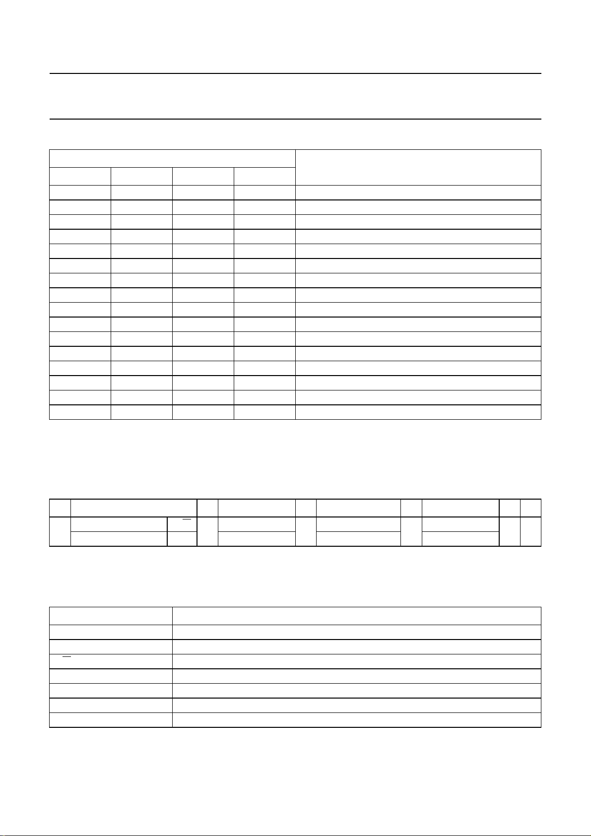
(see Table 7).Also the digital-to-analog converted valueis
given as current at pin AFC.
8.8 Sound carrier trap
The sound carrier trap consists of a reference filter, a
phase detector and the sound trap itself.
A sound carrier reference signal is fed into the reference
low-pass filter and is shifted by nominal 90 degrees. The
phasedetectorcompares the original reference signal with
the signal shifted by the reference filter and produces a
DC voltage by charging or discharging an integrated
capacitor with a current proportional to the phase
difference between both signals, respectively to the
frequency error of the integrated filters. The DC voltage
controls the frequency position of the reference filter and
the sound trap. So the accurate frequency position for the
different standards is set by the sound carrier reference
signal.
The sound trap itself is constructed of three separatetraps
to realize sufficient suppression of the first and second
sound carriers.
8.9 SIF amplifier
The SIF amplifier consists of three AC-coupled differential
stages.Gain control isperformedby emitter degeneration.
The total gain control range is typically 66 dB. The
differentialinputimpedanceistypically2 kΩinparallelwith
3 pF.
2004 Aug 25 11
Page 12

Philips Semiconductors Product specification
I2C-bus controlled multistandard alignment-free
IF-PLL demodulator with FM radio
8.10 SIF-AGC detector
SIF gain control is performed by the detection of the
DC component of the AM demodulator output signal. This
DC signal corresponds directly to the SIF voltage at the
output of the SIF amplifier so that a constant SIF signal is
supplied to the AM demodulator and to the single
reference QSS mixer.
By switching the gain of the inputamplifier of the SIF-AGC
detector via the I2C-bus, the internal SIF level for
FM sound is 5.5 dB lower than for AM sound. This is to
adapt the SIF-AGC characteristic to the VIF-AGC
characteristic. The adaption is ideal for a picture-to-sound
FM carrier ratio of 13 dB.
Viaacomparator, the integrated AGC capacitorischarged
or discharged for the generation of the required SIF gain.
Due to AM sound, the AGC reaction time is slow
(fc< 20 Hz for the closed AGC loop). For reducing this
AM sound time constant in the event of a decreasing
IF amplitude step, the load current of theAGC capacitor is
increased (fast mode) when the VIF-AGC detector (at
positive modulation mode) operates in the fast mode too.
An additional circuit (threshold approximately 7 dB)
ensures a very fast gain reduction for a large increasing
IF amplitude step.
8.11 Single reference QSS mixer
With the present system a high performance Hi-Fi stereo
sound processing can be achieved. For a simplified
application without a SIF SAW filter, the single reference
QSSmixercan be switched to theintercarriermodevia the
I2C-bus.
The single reference QSS mixer generates the 2nd FM
TV sound intercarrier signal. It is realized by a linear
multiplier which multiplies the SIF amplifier output signal
and the VIF-PLL VCO signal (90 degrees output) which is
locked to the picture carrier. In this way the QSS mixer
operates as a quadrature mixer in the intercarrier mode
and provides suppression of the low frequency video
signals.
The QSS mixer output signal is fed internally via a
high-pass and low-pass combination to the
FM demodulator as well as via an operational amplifier to
the intercarrier output pin SIOMAD.
8.12 AM demodulator
The amplitude modulated SIF amplifier output signal is fed
both to a two-stage limiting amplifier that removes the AM
and to a linear multiplier. The result of the multiplication of
the SIF signal with the limiter output signal is
AM demodulation (passive synchronous demodulator).
The demodulator output signal is fed via a low-pass filter
that attenuates the carrier harmonics and via the input
amplifier of the SIF-AGC detector to the audio amplifier.
8.13 FM demodulator and acquisition help
The narrow-band FM-PLL detector consists of:
• Gain controlled FM amplifier and AGC detector
• Narrow-band PLL.
The intercarrier signal from the intercarrier mixer or from
pin FMIN is fed to the input of an AC-coupled gain
controlled amplifier with two stages. The gain controlled
output signal is fed to the phase detector of the
narrow-band FM-PLL (FM demodulator). For good
selectivity and robustness against disturbance caused by
the video signal, a high linearity of the gain controlled
FM amplifier and of the phase detector as well as a
constantsignal level arerequired. The gain control is done
by means of an ‘in phase’ demodulator for the FM carrier
(from the output of the FM amplifier). The demodulation
output is fed into a comparator for charging or discharging
the integrated AGC capacitor. This leads to a mean value
AGC loop to control the gain of the FM amplifier.
The FM demodulator is realized as a narrow-band PLL
with an external loop filter, which provides the necessary
selectivity(bandwidthapproximately 100 kHz). To achieve
good selectivity, a linear phase detector and a constant
input level are required. The gain controlled intercarrier
signal from the FM amplifier is fed to the phase detector.
The phase detector controls via the loop filter the
integratedlowradiation relaxation oscillator. Thedesigned
frequency range is from 4 to 7 MHz.
The VCO within the FM-PLL is phase-locked to the
incoming 2nd SIF signal, which is frequency modulated.
As well as this, the VCO control voltage is superimposed
by the AF voltage. Therefore, the VCO tracks with the FM
of the 2nd SIF signal. So, the AF voltage is present at the
loop filter and is typically 5 mV (RMS) for 27 kHz
FM deviation.This AF signal isfedvia a buffer tothe audio
amplifier.
TDA9887
2004 Aug 25 12
The correct locking of the PLL is supported by the digital
acquisition help circuit (see Section 8.6).
Page 13

Philips Semiconductors Product specification
I2C-bus controlled multistandard alignment-free
IF-PLL demodulator with FM radio
8.14 Audio amplifier and mute time constant
The audio amplifier consists of two parts:
• AF preamplifier
• AF output amplifier.
The AF preamplifier used for FM sound is an operational
amplifier with internal feedback, high gain and high
common mode rejection. The AF voltage from the
PLL demodulator is 5 mV (RMS)for a frequency deviation
of 27 kHz and is amplified by 30 dB. By the use of a
DC operating point control circuit (with external
capacitor CAF), the AF preamplifier is decoupled from the
PLL DC voltage. The low-pass characteristic of the
amplifier reduces the harmonics of the sound intercarrier
signal at the AF output terminal.
For FM sound a switchable de-emphasis network (with
external capacitor) is implemented between the
preamplifier and the output amplifier.
The AF output amplifier provides the required AF output
level by a rail-to-rail output stage. A preceding stage
makes use of an input selector for switching between
FM sound, AM sound and mute state. The gain can be
switched between 10 dB (normal) and 4 dB (reduced).
Switching to the mute state is controlled automatically,
dependent on the digital acquisition help in case the VCO
of the FM-PLL is not in the required frequency window.
This is done by a time constant: fast for switching to the
mute state and slow (typically 40 ms) for switching to the
no-mute state.
All switching functions are controlled via the I2C-bus:
• AM sound, FM sound and forced mute
• Auto mute enable or disable
• De-emphasis off or on with 50 or 75 µs
• Audio gain normal or reduced.
8.15 Radio mode
The principle is to multiply the first radio IF (e.g. 33.3 MHz
at tuner output) with 44 MHz reference signal. The result
of the down-conversion is the second radio IF (10.7 MHz)
at intercarrier output.
In the radio mode the tuner delivers a first radio IF signal
of 33.3 MHz. This signal is fed via the SIF SAW filter
(conventional used for QSS TV sound processing) to the
SIF input. The sound IF amplifier supplies this radio
IF signalbymeansof gain control with constant level tothe
QSSmixer.Thesingle reference QSS mixer generates the
second radio IF signal of 10.7 MHz. In the radio mode the
VIF VCO operates as part of a frequency synthesizer and
delivers a constant 44 MHz signal (derived from the
reference signal of 4 MHz) for the down-conversion of the
firstradio IF to 10.7 MHz.Thissignal is fedviathe external
ceramic band-pass filter to the FM demodulator. The
demodulated AF signal is amplified by the audio amplifier.
In case of NTSC application (M/N standard) the internal
mixingfrequency is 52 MHz.So, the firstradio IF has tobe
41.3 MHz.
In the radio mode, the tuner AGC is derived from the
SIF-AGC.
For tuning search mode, the device offers certain
monitoring functions. Switchable are radio AFC, FM-AGC
or SIF-AGC to pin AFC.
8.16 Internal voltage stabilizer
The band gap circuit internally generates a voltage of
approximately 2.4 V, independent of supply voltage and
temperature. A voltage regulator circuit, connected to this
voltage, produces a constant voltage of 3.55 V which is
used as an internal reference voltage.
8.17 I
The device can be controlled via the 2-wire I2C-bus by a
microcontroller. Two wires carry serial data (SDA) and
serial clock (SCL) information between the devices
connected to the I2C-bus.
The device has an I2C-bus slave transceiver with
auto-increment. The circuit operates up to clock
frequencies of 400 kHz.
A slave address is sent from the master to the slave
receiver. To avoid conflicts in a real application with other
devices providing similar or complementing functions,
there are four possible slave addresses available. These
Module Addresses (MADs)can be selected by connecting
resistors on pin SIOMAD and/or pins SIF1 and SIF2 (see
Fig.25). Pin SIOMAD relates with bit A0 and pins SIF1
and SIF2 relate with bit A3. The slave addresses of this
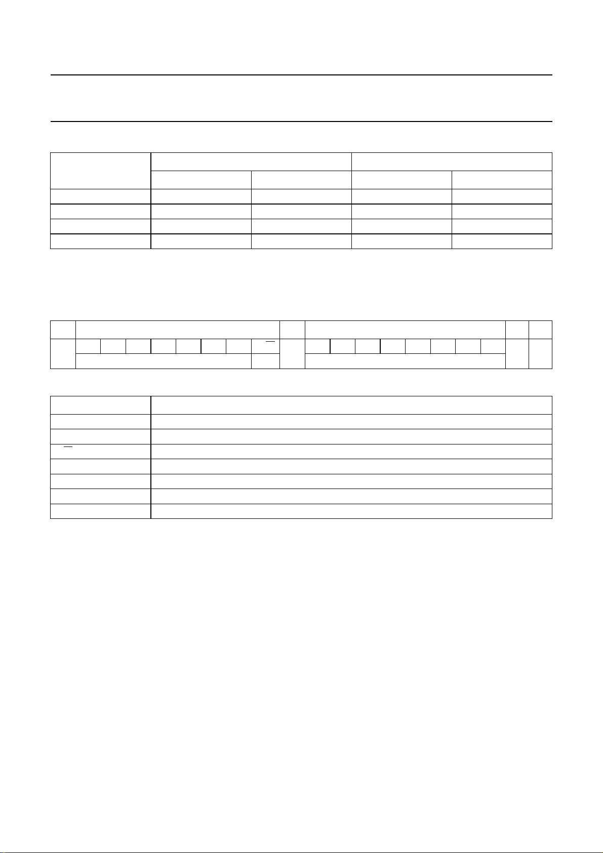
device are given in Table 1.
The power-on preset value is dependent on the use of
pin SIOMAD and can be chosen for 45.75 MHz NTSC as
default(pin SIOMADleftopen-circuit)or 58.75 MHz NTSC
(resistor on pin SIOMAD). In this way the device can be
used without the I2C-bus as an NTSC only device.
Remark: In case of using the device without the I2C-bus,
then the rise time of the supply voltage after switching on
power must be longer than 1.2 µs.
TDA9887
2
C-bus transceiver and module address
2004 Aug 25 13
Page 14
Philips Semiconductors Product specification
I2C-bus controlled multistandard alignment-free
TDA9887
IF-PLL demodulator with FM radio
Table 1 Slave address detection
SLAVE ADDRESS
MAD1 0 1 no no
MAD2 0 0 no yes
MAD3 1 1 yes no
MAD4 1 0 yes yes
2
9I
C-BUS CONTROL
9.1 Read format
2
Table 2 I
S BYTE 1 A BYTE 2 AN P
Table 3 Explanation of Table 2
C-bus read format (slave transmits data)
A6 A5 A4 A3 A2 A1 A0 R/
slave address 1 data
SELECTABLE ADDRESS BIT RESISTOR ON PIN
A3 A0 SIF1 AND SIF2 SIOMAD
W D7D6D5D4D3D2D1D0
SYMBOL FUNCTION
S START condition, generated by the master
Slave address see Table 4
R/W = 1 read command, generated by the master
A acknowledge bit, generated by the slave
Data 8-bit data word, transmitted by the slave (see Table 5)
AN acknowledge-not bit, generated by the master
P STOP condition, generated by the master
The master generates an acknowledge when it has received the dataword READ. The master next generates an
acknowledge, then slave begins transmitting the dataword READ, and so on until the master generates an
acknowledge-not bit and transmits a STOP condition.
2004 Aug 25 14
Page 15

Philips Semiconductors Product specification
I2C-bus controlled multistandard alignment-free
TDA9887
IF-PLL demodulator with FM radio
9.1.1 SLAVE ADDRESS
The first module address MAD1 is the standard address (see Table 1).
Table 4 Slave addresses; notes 1 and 2
SLAVE ADDRESS BIT
NAME
MAD1 43 1 0 0 0 0 1 1
MAD2 42 1 0 0 0 0 1 0
MAD3 4B 1 0 0 1 0 1 1
MAD4 4A 1 0 0 1 0 1 0
Notes
1. For MAD activation via external resistor: see Table 1 and Fig.25.
2. For applications without I2C-bus: see Tables 18 and 19.
9.1.2 DATA BYTE
VALUE
(HEX)
A6 A5 A4 A3 A2 A1 A0
Table 5 Data read register (status register)
MSB LSB
D7 D6 D5 D4 D3 D2 D1 D0
AFCWIN VIFLEV CARRDET AFC4 AFC3 AFC2 AFC1 PONR
Table 6 Description of status register bits
BIT VALUE DESCRIPTION
AFCWIN AFC window
1 VCO in ±1.6 MHz AFC window; note 1
0 VCO out of ±1.6 MHz AFC window
VIFLEV VIF input level
1 high level; VIF input voltage ≥ 200 µV (typically)
0 low level
CARRDET FM carrier detection
1 detection
0 no detection
AFC[4:1] Automatic frequency control
see Table 7
PONR Power-on reset
1 after Power-on reset or after supply breakdown
0 after a successful reading of the status register
Note
1. If no IF input is applied, then bit AFCWIN = 1 due to the fact that the VCO is forced to the AFC window border for
fast lock-in behaviour.
2004 Aug 25 15
Page 16
Philips Semiconductors Product specification
I2C-bus controlled multistandard alignment-free
IF-PLL demodulator with FM radio
Table 7 Automatic frequency control bits; note 1
BIT
AFC4 AFC3 AFC2 AFC1
0111 ≤ (f0− 187.5 kHz)
0110 f
0101 f
0100 f
0011 f
0010 f
0001 f
0000 f
1111 f
1110 f
1101 f
1100 f
1011 f
1010 f
1001 f
1000 ≥ (f0+ 187.5 kHz)
f
VIF
− 162.5 kHz
0
− 137.5 kHz
0
− 112.5 kHz
0
− 87.5 kHz
0
− 62.5 kHz
0
− 37.5 kHz
0
− 12.5 kHz
0
+ 12.5 kHz
0
+ 37.5 kHz
0
+ 62.5 kHz
0
+ 87.5 kHz
0
+ 112.5 kHz
0
+ 137.5 kHz
0
+ 162.5 kHz
0
TDA9887
Note
1. f0is the nominal frequency of f
VIF
.
9.2 Write format
2
Table 8 I
C-bus write format (slave receives data); note 1
S BYTE 1 A BYTE 2 A BYTE 3 A BYTE n A P
A6 to A0 R/
W A7 to A0 bits 7 to 0 bits 7 to 0
slave address 0 subaddress data 1 data n
Note
1. The auto-increment of the subaddress stops if the subaddress is 3.
Table 9 Explanation of Table 8
SYMBOL FUNCTION
S START condition, generated by the master
Slave address see Table 4
R/W = 0 write command, generated by the master
A acknowledge bit, generated by the slave
Subaddress (SAD) see Table 10
Data 1, data n 8-bit data words, transmitted by the master (seeTables 11, 12 and 14)
P STOP condition
2004 Aug 25 16
Page 17

Philips Semiconductors Product specification
I2C-bus controlled multistandard alignment-free
TDA9887
IF-PLL demodulator with FM radio
9.2.1 SUBADDRESS
If more than one data byte is transmitted, then auto-increment is performed: starting from the transmitted subaddress
and auto-increment of subaddress in accordance with the order of Table 10.
Table 10 Definition of the subaddress (second byte after slave address); note 1
REGISTER
SAD for switching mode 0 XXXXX00
SAD for adjust mode 0 XXXXX01
SAD for data mode 0 XXXXX10
Notes
1. X = don’t care.
2. Bit A7 = 1 is not allowed.
3. Bits A6 to A2 will be ignored by the internal hardware.
9.2.2 DATA BYTE FOR SWITCHING MODE
MSB LSB
A7
(2)
A6
(3)
A5
(3)
A4
(3)
A3
(3)
A2
(3)
A1 A0
Table 11 Bit description of SAD register for switching mode (SAD = 00)
BIT VALUE DESCRIPTION
B7 Output port 2 e.g. for SAW switching or AGC monitoring
1 high-impedance, disabled or HIGH
0 low-impedance, active or LOW
B6 Output port 1 e.g. for SAW switching or external AGC input
1 high-impedance, disabled or HIGH
0 low-impedance, active or LOW
B5 Forced audio mute
1on
0 off
B4 and B3 TV standard modulation and radio mode
00 positive AM TV; note 1
01 FM radio; note 2
10 negative FM TV
11 FM radio; note 2
B2 Carrier mode
1 QSS mode
0 intercarrier mode
B1 Auto mute of FM AF output
1 active
0 inactive
2004 Aug 25 17
Page 18

Philips Semiconductors Product specification
I2C-bus controlled multistandard alignment-free
IF-PLL demodulator with FM radio
BIT VALUE DESCRIPTION
B0 Video mode (sound trap)
1 sound trap bypass
0 sound trap active
Notes
1. For positive AM TV choose 6.5 MHz for the second SIF.
2. For FM radio, select f
9.2.3 DATA BYTE FOR ADJUST MODE
Table 12 Bit description of SAD register for adjust mode (SAD = 01)
BIT VALUE DESCRIPTION
C7 Audio gain
C6 De-emphasis time constant
C5 De-emphasis
C4 to C0 Tuner takeover point adjustment
= 45.75 MHz for NTSC applications; otherwise use an arbitrary video IF (see Table 17).
VIF
1 −6dB
00dB
150µs
075µs
1on
0 off
see Table 13
TDA9887
2004 Aug 25 18
Page 19

Philips Semiconductors Product specification
I2C-bus controlled multistandard alignment-free
IF-PLL demodulator with FM radio
Table 13 Tuner takeover point adjustment bits
BIT
C4 C3 C2 C1 C0
11111 +15
11110 +14
11101 +13
11100 +12
11011 +11
11010 +10
11001 +9
11000 +8
10111 +7
10110 +6
10101 +5
10100 +4
10011 +3
10010 +2
10001 +1
10000 0
01111 −1
01110 −2
01101 −3
01100 −4
01011 −5
01010 −6
01001 −7
01000 −8
00111 −9
00110 −10
00101 −11
00100 −12
00011 −13
00010 −14
00001 −15
00000 −16
TDA9887
TOP ADJUSTMENT (dB)
(1)
Note
1. 0 dB is equal to 17 mV (RMS).
2004 Aug 25 19
Page 20

Philips Semiconductors Product specification
I2C-bus controlled multistandard alignment-free
IF-PLL demodulator with FM radio
9.2.4 DATA BYTE FOR DATA MODE
Table 14 Bit description of SAD register for data mode (SAD = 10)
BIT VALUE DESCRIPTION
E7 AGC features
dependent on bit E5; see Tables 15 and 16
E6 L standard PLL gating
1 gating in case of 36 % positive modulation
0 gating in case of 0 % positive modulation
E5 VIF, SIF and tuner minimum gain
dependent on bit E7; see Table 15
E4 to E2 Frequency selection
see Table 17
E1 and E0 Standard frequency sound intercarrier (sound 2nd IF)
00 fFM= 4.5 MHz
01 fFM= 5.5 MHz
10 fFM= 6.0 MHz
11 fFM= 6.5 MHz (for positive modulation choose 6.5 MHz)
TDA9887
Table 15 Options in extended TV mode; bit B3 = 0 of SAD = 00 register
FUNCTION
BIT E5 = 0 BIT E5 = 1 BIT E5 = 0 BIT E5 = 1
Pin OP1 port function port function port function VIF-AGC external input
Pin OP2 port function port function VIF-AGC output
Gain normal gain minimum gain normal gain external gain
Note
1. The corresponding port function has to be disabled (set to ‘high-impedance’); see Table 11 and Chapter 12,
characteristics table, note 12.
Table 16 Options in extended radio mode; bit B3 = 1 of SAD = 00 register
FUNCTION BIT E7 = 0
Pin AFC FM radio carrier related AFC SIF-AGC radio output FM-AGC radio output
BIT E7 = 0 BIT E7 = 1
(1)
BIT E3 = 0 BIT E3 = 1
port function
BIT E7 = 1
(1)
2004 Aug 25 20
Page 21

Philips Semiconductors Product specification
I2C-bus controlled multistandard alignment-free
TDA9887
IF-PLL demodulator with FM radio
Table 17 Frequency selection bits
BIT DESCRIPTION
E4 E3 E2
000f
001f
010f
011f
100f
101f
110f
VIF
VIF
VIF
VIF
VIF
VIF
VIF
BIT B3 = 0 OF REGISTER SAD = 00
= 58.75 MHz; note 1 f
= 45.75 MHz; note 1 f
= 38.9 MHz f
= 38.0 MHz f
= 33.9 MHz f
= 33.4 MHz f
= 45.75 MHz plus FM external input via
TV MODE
BIT B3 = 1 OF REGISTER SAD = 00
= 33.3 MHz, f
RIF1
= 41.3 MHz, f
RIF1
= 33.3 MHz, f
RIF1
= 41.3 MHz, f
RIF1
= 33.3 MHz, f
RIF1
= 33.3 MHz, f
RIF1
f
= 33.3 MHz, f
RIF1
pin FMIN; note 2
111f
= 38.9 MHz plus FM external input via
VIF
f
= 33.3 MHz, f
RIF1
pin FMIN; note 2
Notes
1. Pin SIOMAD can be used for the selection of the different NTSC standards without I2C-bus. With a resistor on
pin SIOMAD, f
= 58.75 MHz; without a resistor on pin SIOMAD, f
VIF
= 45.75 MHz (NTSC-M).
VIF
2. Attention: video sound traps are locked on the FM VCO. The second VIF should be selected in accordance with the
selected video standard.
RADIO MODE
= 44 MHz; f
VCO
= 52 MHz; f
VCO
= 44 MHz; f
VCO
= 52 MHz; f
VCO
= 44 MHz; f
VCO
= 44 MHz; f
VCO
= 44 MHz; f
VCO
= 44 MHz; f
VCO
= 10.7 MHz
RIF2
= 10.7 MHz
RIF2
= 10.7 MHz
RIF2
= 10.7 MHz
RIF2
= 10.7 MHz
RIF2
= 10.7 MHz
RIF2
= 10.7 MHz
RIF2
= 10.7 MHz
RIF2
Table 18 Data setting after power-on reset (default setting with a resistor on pin SIOMAD)
MSB LSB
REGISTER
D7 D6 D5 D4 D3 D2 D1 D0
Switching mode 11010110
Adjust mode 00110000
Data mode 00000000
Table 19 Data setting after power-on reset (default setting without a resistor on pin SIOMAD)
MSB LSB
REGISTER
D7 D6 D5 D4 D3 D2 D1 D0
Switching mode 11010110
Adjust mode 00110000
Data mode 00000100
2004 Aug 25 21
Page 22

Philips Semiconductors Product specification
I2C-bus controlled multistandard alignment-free
TDA9887
IF-PLL demodulator with FM radio
10 LIMITING VALUES
In accordance with the Absolute Maximum Rating System (IEC 60134).
SYMBOL PARAMETER CONDITIONS MIN. MAX. UNIT
V
P
V
n
t
sc
T
stg
T
amb
V
es
Notes
1. Machine model in accordance with SNW-FQ-302B: class C, discharging a 200 pF capacitor via a 0.75 µH series
inductance.
2. Human body model in accordance with SNW-FQ-302A: class 2, discharging a 100 pF capacitor via a 1.5 kΩ series
resistor.
supply voltage − 5.5 V
voltage on
pins VIF1, VIF2, SIF1, SIF2, OP1, OP2, VP, and FMPLL 0 V
P
V
pin TAGC 0 8.8 V
short-circuit time to ground or V
P
− 10 s
storage temperature −25 +150 °C
ambient temperature
TDA9887T (SO24) and TDA9887TS (SSOP24) −20 +70 °C
TDA9887HN (HVQFN32) −20 +85 °C
electrostatic discharge voltage on all pins note 1 −400 +400 V
note 2 −4000 +3500 V
11 THERMAL CHARACTERISTICS
SYMBOL PARAMETER CONDITIONS VALUE UNIT
R
th(j-a)
thermal resistance from junction to ambient in free air
TDA9887T (SO24) 76 K/W
TDA9887TS (SSOP24) 105 K/W
TDA9887HN (HVQFN32) 40 K/W
2004 Aug 25 22
Page 23

Philips Semiconductors Product specification
I2C-bus controlled multistandard alignment-free
TDA9887
IF-PLL demodulator with FM radio
12 CHARACTERISTICS
VP=5V; T
= 33.4 MHz; PC/SC = 13 dB; f
f
SC
for L); IF input from 50 Ω via broadband transformer 1 : 1; video modulation DSB; residual carrier for B/G is 10 % and
for L is 3 %; video signal in accordance with
test circuit of Fig.25; unless otherwise specified.
SYMBOL PARAMETER CONDITIONS MIN. TYP. MAX. UNIT
Supply (pin VP)
V
P
I
P
P
tot
POWER-ON RESET
V
P(start)
V
P(stop)
τ
P
VIF amplifier (pins VIF1 and VIF2)
V
i(VIF)(rms)
V
i(max)(rms)
V
i(ovl)(rms)
∆V
IF(int)
G
VIF(cr)
B
VIF(−3dB)(ll)
B
VIF(−3dB)(ul)
R
i(dif)
C
i(dif)
V
I
FPLL and true synchronous video demodulator; note 4
f
VCO(max)
f
VIF
=25°C; see Table 21 for input frequencies; B/G standard is used for the specification (fPC= 38.9 MHz;
amb
= 400 Hz); input level V
mod
“CCIR line 17 and line 330”or“NTC-7 Composite”
= 10 mV (RMS) (sync level for B/G; peak white level
i(VIF)
; measurements taken in
supply voltage note 1 4.5 5.0 5.5 V
supply current 52 63 70 mA
total power dissipation − 305 385 mW
supply voltage for start of reset decreasing supply
2.5 3.0 3.5 V
voltage
supply voltage for end of reset increasing supply
−−4.4 V
voltage; I2C-bus
transmission enable
time constant (R × C) for
network at pin V
P
VIF input voltage sensitivity
for applications without
1.2 −−µs
I2C-bus
−1 dB video at output − 60 100 µV
(RMS value)
maximum input voltage
+1 dB video at output 150 190 − mV
(RMS value)
overload input voltage
note 2 −−440 mV
(RMS value)
internal IF amplitude difference
between picture and sound
within AGC range;
∆f = 5.5 MHz
− 0.7 − dB
carrier
VIF gain control range 60 66 − dB
lower limit −3 dB VIF bandwidth − 15 − MHz
upper limit −3 dB VIF bandwidth − 80 − MHz
differential input resistance note 3 − 2 − kΩ
differential input capacitance note 3 − 3 − pF
DC input voltage − 1.93 − V
maximum oscillator frequency
f=2f
PC
120 140 − MHz
for carrier regeneration
vision carrier operating
frequencies
see Table 17 − 33.4 − MHz
− 33.9 − MHz
− 38.0 − MHz
− 38.9 − MHz
− 45.75 − MHz
− 58.75 − MHz
2004 Aug 25 23
Page 24

Philips Semiconductors Product specification
I2C-bus controlled multistandard alignment-free
TDA9887
IF-PLL demodulator with FM radio
SYMBOL PARAMETER CONDITIONS MIN. TYP. MAX. UNIT
∆f
VIF
t
acq
V
i(lock)(rms)
T
cy(DAH)
K
O(VIF)
K
D(VIF)
Video output 2 V (pin CVBS)
NORMAL MODE (SOUND CARRIER TRAP ACTIVE) AND SOUND CARRIER ON
V
o(v)(p-p)
∆V
o
V/S ratio between video
V
sync
V
clip(u)
V
clip(l)
R
o
I
bias(int)
I
o(sink)(max)
I
o(source)(max)
∆V
o(CVBS)
∆V
o(bl)
∆V
o(bl)(v)
G
dif
ϕ
dif
S/N
W
VIF frequency window of digital
acquisition help
related to f
see Fig.11
VIF
;
−±2.3 − MHz
acquisition time BL = 70 kHz; note 5 −−30 ms
input voltage sensitivity for PLL
to be locked (RMS value)
measured on pins VIF1
and VIF2;
− 30 70 µV
maximum IF gain
cycle time of digital acquisition
− 64 −µs
help
VIF VCO steepness definition: ∆f
VIF phase detector steepness definition: ∆I
video output voltage
see Fig.5 1.7 2.0 2.3 V
VIF
VPLL
/∆V
/∆ϕ
− 20 − MHz/V
VPLL
− 23 −µA/rad
VIF
(peak-to-peak value)
video output voltage difference difference between
−12 − +12 %
L and B/G standard
1.90 2.33 3.00 −
(black-to-white) and sync level
sync voltage level 1.0 1.2 1.4 V
upper video clipping voltage
VP− 1.1 VP− 1 − V
level
lower video clipping voltage
− 0.7 0.9 V
level
output resistance note 3 −−30 Ω
internal DC bias current for
1.5 2.0 − mA
emitter-follower
maximum AC and DC output
1 −−mA
sink current
maximum AC and DC output
3.9 −−mA
source current
deviation of CVBS output
voltage
50 dB gain control −−0.5 dB
30 dB gain control −−0.1 dB
black level tilt negative modulation −−1%
vertical black level tilt for worst
case in L standard
vision carrier
modulated by test line
−−3%
(VITS) only
differential gain “CCIR 330”; note 6
B/G standard −−5%
L standard −−7%
differential phase “CCIR 330” − 2 4 deg
weighted signal-to-noise ratio weighted in accordance
with
“CCIR 567”
;
56 59 − dB
see Fig.13; note 7
2004 Aug 25 24
Page 25

Philips Semiconductors Product specification
I2C-bus controlled multistandard alignment-free
TDA9887
IF-PLL demodulator with FM radio
SYMBOL PARAMETER CONDITIONS MIN. TYP. MAX. UNIT
S/N
UW
α
IM(blue)
α
IM(yellow)
∆V
r(PC)(rms)
∆f
unw(p-p)
∆ϕ robustness for modulator
α
H
α
spur
PSRR
CVBS
M/N STANDARD INCLUDING KOREA; see Fig.15
B
v(−3dB)(trap)
α
SC1
α
SC1(60kHz)
α
SC2
α
SC2(60kHz)
t
d(g)(cc)
B/G STANDARD; see Fig.17
B
v(−3dB)(trap)
α
SC1
α
SC1(60kHz)
α
SC2
unweighted signal-to-noise ratio note 7 47 51 − dB
intermodulation attenuation at
‘blue’
see Fig.14; note 8
f = 1.1 MHz 58 64 − dB
f = 3.3 MHz 58 64 − dB
intermodulation attenuation at
‘yellow’
see Fig.14; note 8
f = 1.1 MHz 60 66 − dB
f = 3.3 MHz 59 65 − dB
residual picture carrier
(RMS value)
robustness for unwanted
frequency deviation of picture
carrier (peak-to-peak value)
imbalance
fundamental wave and
harmonics
3 % residual carrier;
50 % serration pulses;
L standard; note 3
0 % residual carrier;
50 % serration pulses;
− 25mV
−−12 kHz
−−3%
L standard;
L-gating = 0 %; note 3
suppression of video signal
harmonics
suppression of spurious
CL< 20 pF; RL>1kΩ;
35 40 − dB
AC load; note 9a
note 9b 40 −−dB
elements
power supply ripple rejection at
pin CVBS
f
= 70 Hz;
ripple
video signal; grey level;
20 25 − dB
positive and negative
modulation; see Fig.6
−3 dB video bandwidth
f
= 4.5 MHz; note 10 3.95 4.05 − MHz
trap
including sound carrier trap
attenuation at first sound carrier f = 4.5 MHz 30 36 − dB
attenuation at first sound carrier
f
± 60 kHz
SC1
attenuation at second sound
f = 4.5 MHz 21 27 − dB
f = 4.724 MHz 21 27 − dB
carrier
attenuation at second sound
carrier f
SC2
± 60 kHz
group delay at colour carrier
frequency
−3 dB video bandwidth
f = 4.724 MHz 15 21 − dB
f = 3.58 MHz;
110 180 250 ns
see Fig.16
f
= 5.5 MHz; note 10 4.90 5.00 − MHz
trap
including sound carrier trap
attenuation at first sound carrier f = 5.5 MHz 30 36 − dB
attenuation at first sound carrier
f
± 60 kHz
SC1
attenuation at second sound
f = 5.5 MHz 24 30 − dB
f = 5.742 MHz 21 27 − dB
carrier
2004 Aug 25 25
Page 26

Philips Semiconductors Product specification
I2C-bus controlled multistandard alignment-free
TDA9887
IF-PLL demodulator with FM radio
SYMBOL PARAMETER CONDITIONS MIN. TYP. MAX. UNIT
α
SC2(60kHz)
t
d(g)(cc)
I STANDARD; see Fig.19
B
v(−3dB)(trap)
α
SC1
α
SC1(60kHz)
α
SC2
α
SC2(60kHz)
t
d(g)(cc)
D/K STANDARD; see Fig.20
B
v(−3dB)(trap)
α
SC1
α
SC1(60kHz)
α
SC2
α
SC2(60kHz)
t
d(g)(cc)
Video output 1.1 V (pin CVBS)
attenuation at second sound
carrier f
SC2
± 60 kHz
group delay at colour carrier
frequency
−3 dB video bandwidth
f = 5.742 MHz 15 21 − dB
f = 4.43 MHz;
110 180 250 ns
see Fig.18
f
= 6.0 MHz; note 10 5.40 5.50 − MHz
trap
including sound carrier trap
attenuation at first sound carrier f = 6.0 MHz 26 32 − dB
attenuation at first sound carrier
f
± 60 kHz
SC1
attenuation at second sound
f = 6.0 MHz 20 26 − dB
f = 6.55 MHz 12 18 − dB
carrier
attenuation at second sound
carrier f
SC2
± 60 kHz
group delay at colour carrier
f = 6.55 MHz 10 15 − dB
f = 4.43 MHz − 90 160 ns
frequency
−3 dB video bandwidth
f
= 6.5 MHz; note 10 5.50 5.95 − MHz
trap
including sound carrier trap
attenuation at first sound carrier f = 6.5 MHz 26 32 − dB
attenuation at first sound carrier
f
± 60 kHz
SC1
attenuation at second sound
f = 6.5 MHz 20 26 − dB
f = 6.742 MHz 18 24 − dB
carrier
attenuation at second sound
carrier f
SC2
± 60 kHz
group delay at colour carrier
f = 6.742 MHz 13 18 − dB
f = 4.28 MHz − 60 130 ns
frequency
TRAP BYPASS MODE AND SOUND CARRIER OFF; note 11
V
o(v)(p-p)
video output voltage
see Fig.5 0.95 1.10 1.25 V
(peak-to-peak value)
V
V
sync
clip(u)
sync voltage level 1.35 1.5 1.6 V
upper video clipping voltage
level
V
clip(l)
lower video clipping voltage
level
B
v(−1dB)
−1 dB video bandwidth CL< 20 pF; RL>1kΩ;
AC load
B
v(−3dB)
−3 dB video bandwidth CL< 20 pF; RL>1kΩ;
AC load
2004 Aug 25 26
3.5 3.6 − V
− 0.9 1.0 V
56− MHz
78− MHz
Page 27

Philips Semiconductors Product specification
I2C-bus controlled multistandard alignment-free
TDA9887
IF-PLL demodulator with FM radio
SYMBOL PARAMETER CONDITIONS MIN. TYP. MAX. UNIT
S/N
W
S/N
UW
VIF-AGC; note 12
t
resp(inc)
t
resp(dec)
∆V
i(VIF)
V
VAGC
CR
stps
V
th(VIF)
PIN VAGC
I
ch(max)
I
ch(add)
I
dch
Tuner AGC (pin TAGC); see Figs 7 to 10
V
i(VIF)(start1)(rms)
V
i(VIF)(start2)(rms)
weighted signal-to-noise ratio weighted in accordance
with
“CCIR 567”
;
56 59 − dB
see Fig.13; note 7
unweighted signal-to-noise ratio note 7 48 52 − dB
AGC response time to an
increasing VIF step
negative modulation;
20 dB; note 13
positive modulation;
− 4 − ms
− 2.6 − ms
20 dB; note 13
AGC response time to a
decreasing VIF step
negative modulation;
20 dB; note 13
positive modulation;
− 3 − ms
− 890 − ms
20 dB; note 13
L standard; fast mode − 2.6 − ms/dB
L standard; normal
− 143 − ms/dB
mode; note 13
VIF amplitude step for activating
L standard −2 −6 −10 dB
AGC fast mode
gain control voltage range 0.8 − 3.5 V
control steepness definition:
∆G
/∆V
VIF
V
=2to3V
VAGC
threshold voltage for high level
see Tables 5 and 6 120 200 320 µV
VAGC
;
−−80 − dB/V
VIF input
maximum charge current L standard − 100 −µA
additional charge current L standard: in the event
− 100 − nA
of missing VITS pulses
and no white video
content
discharge current L standard; normal
− 35 − nA
mode
L standard; fast mode − 1.8 −µA
VIF input signal voltage for
minimum starting point of tuner
takeover at pins VIF1 and VIF2
(RMS value)
VIF input signal voltage for
maximum starting point of tuner
takeover at pins VIF1 and VIF2
(RMS value)
I
= 120 µA;
TAGC
R
=22kΩ or
TOP
no R
and−15 dBvia
TOP
I2C-bus (see Table 13)
I
= 120 µA;
TAGC
R
=0Ω or no R
TOP
TOP
and +15 dB via I2C-bus
(see Table 13)
− 25mV
45 90 − mV
2004 Aug 25 27
Page 28

Philips Semiconductors Product specification
I2C-bus controlled multistandard alignment-free
TDA9887
IF-PLL demodulator with FM radio
SYMBOL PARAMETER CONDITIONS MIN. TYP. MAX. UNIT
V
i(SIF)(start1)(rms)
V
i(SIF)(start2)(rms)
QV
TOP
∆QV
V
V
I
sink
∆G
/∆T takeover point variation with
TOP
o
sat
IF
AFC circuit and AGC monitor options (pin AFC); see Figs 11 and 12; notes 14 and 15
V
sat(ul)
V
sat(ll)
I
o(source)
I
o(sink)
TV MODE
AFC
stps
Qf
VIF(a)
Qf
VIF(d)
RADIO MODE
AFC
stps
Qf
RIF(a)
Qf
RIF(d)
I
o(source)
I
o(sink)
SIF input signal voltage for
minimum starting point of tuner
takeover at pins SIF1 and SIF2
(RMS value)
SIF input signal voltage for
maximum starting point of tuner
takeover at pins SIF1 and SIF2
(RMS value)
tuner takeover point accuracy I
I
= 120 µA;
TAGC
R
=22kΩ or
TOP
no R
and−15 dBvia
TOP
I2C-bus (see Table 13)
I
= 120 µA;
TAGC
R
=0Ω or no R
TOP
TOP
and +15 dB via I2C-bus
(see Table 13)
= 120 µA;
TAGC
R
=10kΩ or
TOP
no R
and 0 dB via
TOP
− 1 2.5 mV
22.5 45 − mV
7 1743mV
I2C-bus (see Table 13)
I
= 120 µA − 0.03 0.07 dB/K
TAGC
temperature
permissible output voltage from external source −−8.8 V
saturation voltage I
sink current notuner gain reduction;
IF slip by automatic gain control tuner gain current from
= 450 µA −−0.5 V
TAGC
−−0.75 µA
V
= 8.8 V
TAGC
maximum tuner gain
reduction; V
TAGC
=1V
450 600 750 µA
358dB
20 % to 80 %
upper limit saturation voltage VP− 0.6 VP− 0.3 − V
lower limit saturation voltage − 0.3 0.6 V
output source current 160 200 240 µA
output sink current 160 200 240 µA
AFC control steepness definition: ∆I
analog accuracy of AFC circuit I
digital accuracy of AFC circuit
via I2C-bus
= 0; f
AFC
I
= 0; f
AFC
1 digit = 25 kHz
AFC control steepness definition: ∆I
analog accuracy of AFC circuit I
digital accuracy of AFC circuit
via I2C-bus
SIF or FM-AGC monitor source
= 0; f
AFC
I
= 0; f
AFC
1 digit = 25 kHz
see Table 16 −−600 µA
/∆f
AFC
= 4 MHz −20 − +20 kHz
REF
= 4 MHz;
REF
/∆f
AFC
= 4 MHz −10 − +10 kHz
REF
= 4 MHz;
REF
0.85 1.05 1.25 µA/kHz
VIF
−20
− 1 digit
0.85 1.05 1.25 µA/kHz
RIF
−10
− 1 digit
− +20
+ 1 digit
− +10
+ 1 digit
current
SIF or FM-AGC monitor sink
see Table 16 −−270 µA
current
kHz
kHz
2004 Aug 25 28
Page 29

Philips Semiconductors Product specification
I2C-bus controlled multistandard alignment-free
TDA9887
IF-PLL demodulator with FM radio
SYMBOL PARAMETER CONDITIONS MIN. TYP. MAX. UNIT
SIF amplifier (pins SIF1 and SIF2)
V
i(SIF)(rms)
V
i(max)(rms)
V
i(ovl)(rms)
G
SIF(cr)
B
SIF(−3dB)(ll)
B
SIF(−3dB)(ul)
R
i(dif)
C
i(dif)
V
I
SIF-AGC detector
t
resp
Single reference QSS intercarrier mixer (pin SIOMAD)
V
o(intc)(rms)
B
intc(−3dB)(ul)
∆V
r(SC)(rms)
SIF input voltage sensitivity
(RMS value)
FM mode; −3 dB at
intercarrier output
− 30 70 µV
pin SIOMAD
AM mode; −3 dB at
− 70 100 µV
AF output pin AUD
maximum input voltage
(RMS value)
FM mode; 1 dB at
intercarrier output
50 70 − mV
pin SIOMAD
AM mode; 1 dB at
80 140 − mV
AF output pin AUD
overload input voltage
note 2 −−320 mV
(RMS value)
SIF gain control range FM and AM mode 60 66 − dB
lower limit −3 dB SIF bandwidth − 15 − MHz
upper limit −3 dB SIF bandwidth − 80 − MHz
differential input resistance note 3 − 2 − kΩ
differential input capacitance note 3 − 3 − pF
DC input voltage − 1.93 − V
AGC response time to an
increasing or decreasing SIF
step of 20 dB
FM or AM fast step
increasing − 8 − ms
decreasing − 25 − ms
AM slow step
increasing − 80 − ms
decreasing − 250 − ms
IF intercarrier output level
(RMS value)
QSS mode;
SC1;SC2off
L standard;
90 140 180 mV
90 140 180 mV
without modulation
intercarrier mode;
− 75 − mV
PC/SC1= 20 dB;
SC2off; note 16
upper limit −3 dB intercarrier
12 15 − MHz
bandwidth
residual sound carrier
(RMS value)
fundamental wave and
harmonics
QSS mode − 25mV
intercarrier mode − 25mV
2004 Aug 25 29
Page 30

Philips Semiconductors Product specification
I2C-bus controlled multistandard alignment-free
TDA9887
IF-PLL demodulator with FM radio
SYMBOL PARAMETER CONDITIONS MIN. TYP. MAX. UNIT
∆V
r(PC)(rms)
α
H
R
o
V
O
I
bias(int)
I
o(sink)(max)
I
o(source)(max)
I
o(source)
FM-PLL demodulator; notes 15 and 18 to 22
residual picture carrier
(RMS value)
fundamental wave and
harmonics
QSS mode − 25mV
intercarrier mode − 520mV
suppression of video signal
harmonics
intercarrier mode;
f
= 5 MHz
video
35 40 − dB
output resistance note 3 −−30 Ω
DC output voltage − 2 − V
internal DC bias current for
0.90 1.15 − mA
emitter follower
maximum AC output sink
0.6 0.8 − mA
current
maximum AC output source
0.6 0.8 − mA
current
DC output source current MAD2 activated;
0.75 0.93 1.20 mA
note 17
SOUND INTERCARRIER OUTPUT (PIN SIOMAD)
V
FM(rms)
IF intercarrier level for gain
controlled operation of FM-PLL
(RMS value)
V
FM(lock)(rms)
IF intercarrier level for lock-in of
PLL (RMS value)
V
FM(det)(rms)
IF intercarrier level for
FM carrier detect (RMS value)
f
FM
sound intercarrier operating
FM frequencies
IF INTERCARRIER INPUT (PIN FMIN)
V
i(FM)(rms)
IF intercarrier input voltage for
gain controlled operation of
FM-PLL (RMS value)
V
FM(lock)(rms)
IF intercarrier level for lock-in of
PLL (RMS value)
V
FM(det)(rms)
IF intercarrier level for
FM carrier detect (RMS value)
corresponding PC/SC
3.2 − 320 mV
ratio at input pins VIF1
and VIF2 is 7 to 47 dB
−−2mV
see Table 6 −−2.3 mV
see Tables 11 and 14 − 4.5 − MHz
− 5.5 − MHz
− 6.0 − MHz
− 6.5 − MHz
− 10.7 − MHz
radio mode and
1 − 100 mV
FM external mode;
see Table 16
−−0.7 mV
see Table 6 −−0.8 mV
2004 Aug 25 30
Page 31

Philips Semiconductors Product specification
I2C-bus controlled multistandard alignment-free
TDA9887
IF-PLL demodulator with FM radio
SYMBOL PARAMETER CONDITIONS MIN. TYP. MAX. UNIT
AUDIO OUTPUT (PIN AUD)
V
o(AF)(rms)
V
o(AF)(cl)(rms)
∆V
/∆T AFoutput voltage variation with
o(AF)
THD total harmonic distortion 50 µs de-emphasis;
∆f
AF
B
AF(−3dB)
S/N
W(AF)
S/N
UW(AF)
∆V
r(SC)(rms)
α
AM(sup)
PSRR
FM
FM-PLL FILTER (PIN FMPLL)
V
loop
I
o(source)(PD)(max)
I
o(sink)(PD)(max)
AF output voltage (RMS value) 25 kHz FM deviation;
400 500 600 mV
75 µs de-emphasis
27 kHz FM deviation;
430 540 650 mV
50 µs de-emphasis
radio mode; 22.5 kHz
200 250 300 mV
modulation
AF output clipping level
THD < 1.5 % 1.3 1.4 − V
(RMS value)
− 3 × 10−37 × 10−3dB/K
temperature
− 0.15 0.50 %
FM deviation: for
TV mode 27 kHz and
for radio mode
22.5 kHz
frequency deviation THD < 1.5 %; note 19 −−±55 kHz
−6 dB AF output via
−−±110 kHz
I2C-bus; note 19
−3 dB AF bandwidth without de-emphasis;
80 100 − kHz
measured with FM-PLL
filter of Fig.25
weighted signal-to-noise ratio of
audio signal
FM-PLL only;
27 kHz FM deviation;
52 56 − dB
50 µs de-emphasis
black picture;
50 56 − dB
see Fig.21
unweighted signal-to-noise ratio radio mode; 22.5 kHz
− 58 − dB
modulation
residual sound carrier
(RMS value)
fundamental wave and
harmonics; without
−−2mV
de-emphasis
AM suppression of
FM demodulator
referenced to 27 kHz
FM deviation;
40 46 − dB
50 µs de-emphasis;
AM: f = 1 kHz;
m = 54 %
power supply ripple rejection f
ripple
= 70 Hz;
14 20 − dB
see Fig.6
DC loop voltage 1.5 − 3.3 V
maximumphasedetector output
− 60 −µA
source current
maximumphasedetector output
− 60 −µA
sink current
2004 Aug 25 31
Page 32

Philips Semiconductors Product specification
I2C-bus controlled multistandard alignment-free
TDA9887
IF-PLL demodulator with FM radio
SYMBOL PARAMETER CONDITIONS MIN. TYP. MAX. UNIT
I
o(source)(DAH)
I
o(sink)(DAH)
t
W(DAH)
T
cy(DAH)
K
O(FM)
K
D(FM)
Audio amplifier
DE-EMPHASIS NETWORK (PIN DEEM)
R
o
V
AF(rms)
V
O
AF DECOUPLING (PIN AFD)
V
dec
I
L
I
ch(max)
I
dch(max)
AUDIO OUTPUT (PIN AUD)
R
o
V
O(AUD)
R
L
R
L(DC)
C
L
B
AF(−3dB)(ul)
B
AF(−3dB)(ll)
α
mute
∆V
jump
output source current of digital
− 55 −µA
acquisition help
output sink current of digital
− 55 −µA
acquisition help
pulse width of digital acquisition
− 16 −µs
help current
cycle time of digital acquisition
− 64 −µs
help
VCO steepness definition: ∆fFM/∆V
phase detector steepness definition: ∆I
/∆ϕFM− 4 −µA/rad
FMPLL
output resistance 50 µs de-emphasis;
− 3.3 − MHz/V
FMPLL
4.4 5.0 5.6 kΩ
see Table 12
75 µs de-emphasis;
6.6 7.5 8.4 kΩ
see Table 12
audio signal (RMS value) fAF= 400 Hz;
V
= 500 mV
AUD
− 170 − mV
DC output voltage − 2.37 − V
DC decoupling voltage dependent on f
FM
1.5 − 3.3 V
intercarrier frequency
leakage current ∆V
< ±50 mV −−±25 nA
O(AUD)
maximum charge current 1.15 1.50 1.85 µA
maximum discharge current 1.15 1.50 1.85 µA
output resistance note 3 −−300 Ω
DC output voltage − 2.37 − V
load resistance AC-coupled 10 −−kΩ
DC load resistance 100 −−kΩ
load capacitance −−1.5 nF
upper limit −3 dB AF bandwidth
150 −−kHz
of audio amplifier
lower limit −3 dB AF bandwidth
note 20 −−20 Hz
of audio amplifier
mute attenuation of AF signal via I2C-bus 70 75 − dB
DC jump voltage for switching
AF output to mute state or vice
versa
activated by digital
acquisition help or via
I2C-bus mute
−±50 ±150 mV
2004 Aug 25 32
Page 33

Philips Semiconductors Product specification
I2C-bus controlled multistandard alignment-free
TDA9887
IF-PLL demodulator with FM radio
SYMBOL PARAMETER CONDITIONS MIN. TYP. MAX. UNIT
FM operation; notes 21 and 23
INTERCARRIER AF PERFORMANCE; note 24
S/N
W
SINGLE REFERENCE QSS AF PERFORMANCE; notes 25 and 26
S/N
W(SC1)
weighted signal-to-noise ratio PC/SC ratio is 21 to
27 dB at pins VIF1 and
VIF2
black picture 50 56 − dB
white picture 45 51 − dB
6 kHz sine wave
(black-to-white
modulation)
sound carrier
subharmonics;
f = 2.75 MHz ±3 kHz
weighted signal-to-noise ratio
for SC
1
PC/SC1 ratio at
pins VIF1 and VIF2;
27 kHz (54 % FM
deviation);
black picture 53 58 − dB
white picture 50 53 − dB
6 kHz sine wave
(black-to-white
modulation)
250 kHzsquarewave
(black-to-white
modulation)
sound carrier
subharmonics;
f = 2.75 MHz ±3 kHz
sound carrier
subharmonics;
f = 2.87 MHz ±3 kHz
“CCIR 468”
40 46 − dB
35 40 − dB
40 −−dB
44 48 − dB
40 45 − dB
45 51 − dB
46 52 − dB
2004 Aug 25 33
Page 34

Philips Semiconductors Product specification
I2C-bus controlled multistandard alignment-free
TDA9887
IF-PLL demodulator with FM radio
SYMBOL PARAMETER CONDITIONS MIN. TYP. MAX. UNIT
S/N
W(SC2)
AM operation
weighted signal-to-noise ratio
for SC
2
PC/SC2 ratio at
40 −−dB
pins VIF1 and VIF2;
27 kHz (54 % FM
deviation);
“CCIR 468”
black picture 48 55 − dB
white picture 46 51 − dB
6 kHz sine wave
42 46 − dB
(black-to-white
modulation)
250 kHzsquarewave
29 34 − dB
(black-to-white
modulation)
sound carrier
44 50 − dB
subharmonics;
f = 2.75 MHz ±3 kHz
sound carrier
45 51 − dB
subharmonics;
f = 2.87 MHz ±3 kHz
L STANDARD (PIN AUD); see Figs 22 and 23; note 27
V
o(AF)(rms)
AF output voltage (RMS value) 54 % modulation 400 500 600 mV
THD total harmonic distortion 54 % modulation − 0.5 1.0 %
B
AF(−3dB)
S/N
W(AF)
V
O(AUD)
PSRR
AM
−3 dB AF bandwidth 100 125 − kHz
weighted signal-to-noise ratio of
audio signal
in accordance with
“CCIR 468”
45 50 − dB
DC potential voltage − 2.37 − V
power supply ripple rejection see Fig.6 20 26 − dB
Reference frequency input (pin REF)
V
I
R
i
R
xtal
DC input voltage 2.3 2.6 2.9 V
input resistance note 3 − 5 − kΩ
resonance resistance of crystal operation as crystal
−−200 Ω
oscillator
C
f
∆f
x
ref
ref
pull-up/down capacitance note 28 −−−pF
reference signal frequency note 29 − 4 − MHz
tolerance of reference signal
note 15 −−±0.1 %
frequency
V
ref(rms)
R
o(ref)
reference signal voltage
(RMS value)
output resistance of reference
operation as input
terminal
80 − 400 mV
−−4.7 kΩ
signal source
C
K
decoupling capacitance to
external reference signal source
operation as input
terminal
22 100 − pF
2004 Aug 25 34
Page 35

Philips Semiconductors Product specification
I2C-bus controlled multistandard alignment-free
TDA9887
IF-PLL demodulator with FM radio
SYMBOL PARAMETER CONDITIONS MIN. TYP. MAX. UNIT
2
I
C-bus transceiver (pins SDA and SCL); notes 30 and 31
f
SCL
V
IH
V
IL
I
IH
I
IL
V
OL
I
o(sink)
I
o(source)
Output ports (pins OP1 and OP2); note 32
V
OL
V
OH
I
o(sink)
I
o(sink/source)(max)
SCL clock frequency 0 − 400 kHz
HIGH-level input voltage 3 − V
CC
LOW-level input voltage −0.3 − +1.5 V
HIGH-level input current −10 − +10 µA
LOW-level input current −10 − +10 µA
LOW-level output voltage IOL=3mA −−0.4 V
output sink current VP=0V −−10 µA
output source current VP=0V −−10 µA
LOW-level output voltage IOL= 2 mA (sink
−−0.4 V
current)
HIGH-level output voltage −−6V
output sink current −−2mA
maximum output sink or source
current
pin OP2 functions as
VIF-AGC output
−−10 µA
V
Notes
1. Values of video and sound parameters can be decreased at VP= 4.5 V.
2. Level headroom for input level jumps during gain control setting.
3. This parameter is not tested during the production and is only given as application information for designing the
receiver circuit.
4. Loop bandwidth BL = 70 kHz (damping factor d = 1.9; calculated with sync level within gain control range).
Calculation of the VIF-PLL filter can be done by use of the following formula:
1
BL
d
3dB–
1
-- 2
K
R=
------ 2π
RKOKDC=
, valid for d ≥ 1.2
OKD
,
where:
rad
is the VCO steepness or ; KDis the phase detector steepness ;
K
O
--------
V
2π
R is the loop resistor; C is the loop capacitor; BL
5. V
= 10 mV (RMS); ∆f = 1 MHz (VCO frequency offset related to picture carrier frequency); white picture video
i(VIF)
Hz
------ V
is the loop bandwidth for −3 dB; d is the damping factor.
−3dB
µA
--------
rad
modulation.
6. Condition: luminance range (5 steps) from 0 % to 100 %.
7. S/N is the ratio of black-to-white amplitude to the black level noise voltage (RMS value on pin CVBS). B = 5 MHz
(B/G, I and D/K standard). Noise analyzer setting: 200 kHz high-pass and SC-trap switched on.
8. The intermodulation figures are defined for:
a) f = 1.1 MHz (referenced to black and white signal) as
b) f = 3.3 MHz (referenced to colour carrier) as
α
IM
2004 Aug 25 35
at 4.4 MHz
V
0
α
IM
V
log=
20
-------------------------------------
V0at 3.3 MHz
20
-------------------------------------
V0at 1.1 MHz
at 4.4 MHz
0
3.6 dB+log=
Page 36

Philips Semiconductors Product specification
I2C-bus controlled multistandard alignment-free
TDA9887
IF-PLL demodulator with FM radio
9. Measurements taken with SAW filter M1963M (sound shelf: 20 dB); loop bandwidth BL = 70 kHz.
a) Modulation Vestigial Side-Band (VSB); sound carrier off; f
b) Sound carrier on; f
= 10 kHz to 10 MHz.
video
10. AC load; CL< 20 pF and RL>1kΩ. The sound carrier frequencies (depending on TV standard) are attenuated by
the integrated sound carrier traps (see Figs 15 to 20; H (s) is the absolute value of transfer function).
11. The sound carrier trap can be bypassed by switching the I2C-bus. In this way the full composite video spectrum
appears at pin CVBS. The amplitude is 1.1 V (p-p).
12. If selected by the I2C-bus, the VIF-AGC voltage can be monitored at pin OP2, and pin OP1 can be used as input. In
this case, both pins cannot be used for the normal port function.
13. The response time is valid for a VIF input level range from 200 µVto70mV.
14. To match the AFC output signal to different tuning systems a current source output is provided. The test circuit is
given in Fig.11. The AFC steepness can be changed by resistors R1 and R2.
15. The tolerance of the reference frequency determines the accuracy of the VIF-AFC, FM demodulator centre
frequency and maximum FM deviation.
16. The intercarrier output signal at pin SIOMAD can be calculated by the following formula taking into account the
internal video signal with 1.1 V (p-p) as a reference:
V
o(intc)(rms)
and
1
r
×=
------
20
1.1
V
i(SC)
-------------V
i(PC)
× 10r×=
---------- 22
1
dB()6 dB 3 dB±+
V
where:
1
is the correction term for RMS value, is the sound-to-picture carrier ratio at pins VIF1 and VIF2
---------- 22
V
iSC()
--------------V
iPC()
dB()
in dB, 6 dB isthe correction termof internal circuitry and ±3 dB is the toleranceof video outputand intercarrier output
V
o(intc)(rms)
17. For normal operation (with the I
.
2
C-bus) no DC load at pin SIOMAD is allowed. The second module address (MAD2)
will be activated by the application of a 2.2 kΩ resistor between pin SIOMAD and ground. If this MAD2 is activated,
also the power-on set-up state activates a VIF frequency of 58.75 MHz.
18. SIF input level is 10 mV (RMS); VIF input level is 10 mV (RMS) unmodulated.
19. Measured with an FM deviation of 25 kHz and the typical AF output voltage of 500 mV (RMS). The AF output signal
canbe attenuated by 6 dB to250 mV (RMS)viathe I2C-bus.For handling a frequency deviationofmorethan 55 kHz,
the AF output signal has to be reduced in order to avoid clipping (THD < 1.5 %).
20. The lower limit of the audio bandwidth depends on the value of the capacitor at pin AFD. A value of CAF= 470 nF
leads to f
AF(−3dB)
≈ 20 Hz and CAF= 220 nF leads to f
AF(−3dB)
21. For all S/N measurements the VIF modulator in use has to meet the following specifications:
a) Incidental phase modulation for black-to-white jump less than 0.5 degrees.
b) QSSAF performance, measured with the television demodulator AMF2 (audio output, weighted S/N ratio) better
than 60 dB (at deviation 27 kHz) for 6 kHz sine wave black-to-white video modulation.
c) Picture-to-sound carrier ratio PC/SC1= 13 dB (transmitter).
> 0.5 MHz.
video
≈ 40 Hz.
2004 Aug 25 36
Page 37

Philips Semiconductors Product specification
I2C-bus controlled multistandard alignment-free
TDA9887
IF-PLL demodulator with FM radio
22. Calculation of the loop filter parameters can be done approximately using the following formulae:
KOK
1
f
------ -
o
2π
ϑ
=
-----------------------------------2R K
BL
3dB–
The formulae are only valid under the following conditions:
ϑ≤1 and C
where:
K
is the VCO steepness or ;
O
is the phase detector steepness ;
K
D
R is the loop resistor;
C
is the series capacitor;
S
C
is the parallel capacitor;
P
is the natural frequency of the PLL;
f
o
BL
is the loop bandwidth for −3 dB;
−3dB
ϑ is the damping factor. For examples, see Table 20.
23. The PC/SC ratio iscalculatedas the addition ofTV transmitterPC/SC
ratio is necessary to achieve the S/NW values as noted. A different PC/SC ratio will change these values.
24. Measurements taken with SAW filter G1984 (Siemens) for vision and sound IF (sound shelf: 14 dB).
Picture-to-sound carrier ratio of transmitter PC/SC = 13 dB. Input level on pins VIF1 and VIF2 of
V
= 10 mV (RMS)sync level, 27 kHz FM deviationfor sound carrier, fAF= 400 Hz.Measurements in accordance
i(SIF)
with
“CCIR 468”
25. The QSS signal output on pin SIOMAD is analysed by a test demodulator TDA9820. The S/N ratio of this device is
more than 60 dB, related to a deviation of ±27 kHz, in accordance with
26. Measurements taken with SAW filter K3953 for vision IF (suppressed sound carrier) and K9453 for sound IF
(suppressed picture carrier). Input level V
27. Measurements taken with SAW filter K9453 (Siemens) for AM sound IF (suppressed picture carrier).
28. The value of Cxdetermines the accuracy of the resonance frequency of the crystal. It depends on the type of crystal
used.
29. Pin REF is able to operate as a 1-pin crystal oscillator input as well as an external reference signal input, e.g. from
the tuning system.
30. The SDA and SCL lines will not be pulled down if VCC is switched off.
31. The AC characteristics are in accordance with the I2C-bus specification for fast mode (maximum clock frequency is
400 kHz). Information about the I2C-bus can be found in the brochure
9398 393 40011).
32. Port P1 and port P2 are open-collector outputs.
D
---------------=
C
P
1
OKDCP
fo1.55 ϑ2–()=
>5C
S
P
. De-emphasis is 50 µs.
rad
--------
V
Hz
2π
------ -
V
µA
--------
rad
= 10 mV (RMS), 27 kHz (54 % FM deviation).
i(SIF)
ratioand SAW filter PC/SC1ratio.This PC/SC
1
“CCIR 468”
“The I2C-bus and how to use it”
.
(order number
2004 Aug 25 37
Page 38

Philips Semiconductors Product specification
I2C-bus controlled multistandard alignment-free
IF-PLL demodulator with FM radio
Table 20 Examples to note 22 (FM-PLL filter)
BL
Table 21 Input frequencies and carrier ratios
DESCRIPTION SYMBOL
VIF carrier f
SIF carrier f
Picture-to-sound
carrier ratio
(kHz) CS(nF) CP(pF) R (kΩ) ϑ
−3dB
100 10 390 5.6 0.5
160 10 150 9.1 0.5
SC1
f
SC2
SC
SC
PC
B/G
STANDARD
38.9 45.75 or 58.75 38.9 33.9 MHz
33.4 41.25 or 54.25 32.4 40.4 MHz
33.158 −−−MHz
1
2
13 7 10 10 dB
20 −−−dB
M/N
STANDARDLSTANDARD
TDA9887
L ACCENT
STANDARD
UNIT
2004 Aug 25 38
Page 39
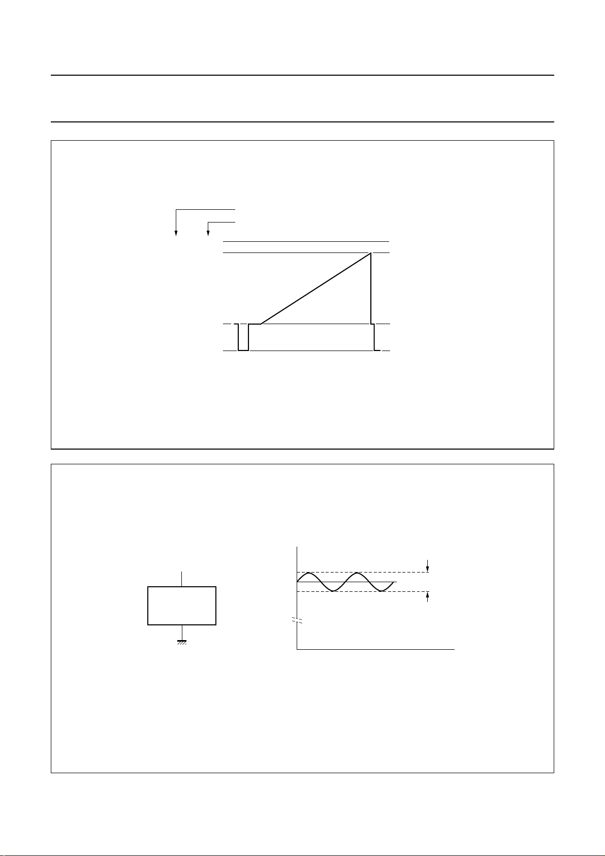
Philips Semiconductors Product specification
I2C-bus controlled multistandard alignment-free
IF-PLL demodulator with FM radio
handbook, full pagewidth
2.72 V
2.6 V
1.83 V
1.5 V
3.41 V
3.20 V
1.80 V
1.20 V
trap bypass mode
normal mode
TDA9887
zero carrier level
white level
black level
sync level
MHC115
handbook, full pagewidth
Fig.5 Typical video signal levels on output pin CVBS (sound carrier off).
V
P
VP = 5 V
TDA9887
MHC145
(V)
5
f
= 70 Hz
ripple
100 mV
t (s)
Fig.6 Ripple rejection condition.
2004 Aug 25 39
Page 40
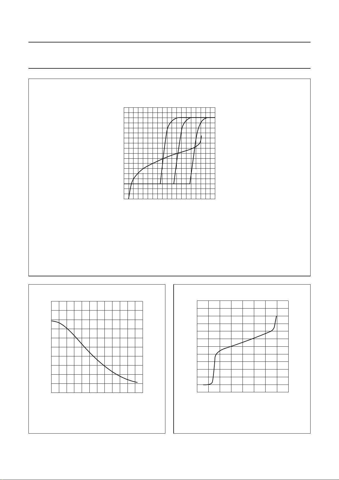
Philips Semiconductors Product specification
I2C-bus controlled multistandard alignment-free
IF-PLL demodulator with FM radio
V
VAGC
(V)
4
3
V
(4)(2) (3)(1)
i(VIF)
2
1
30 40
60
50
70 80 90 100 110
mhc116
120
(dBµV)
I
600
500
400
300
200
100
0
TDA9887
TAGC
(µA)
(1) V
(2) I
(3) I
(4) I
is VIF-AGC voltage and can only be measured at pin OP2 controlled by the I2C-bus (see Table 15).
VAGC
is tuner current in TV mode with R
TAGC
is tuner current in TV mode with R
TAGC
is tuner current in TV mode with R
TAGC
=22kΩ or setting via I2C-bus at −15 dB.
TOP
=10kΩ or setting via I2C-bus at 0 dB.
TOP
=0kΩ or setting via I2C-bus at +15 dB.
TOP
Fig.7 Typical VIF and tuner AGC characteristic.
R
TOP
mhb159
handbook, halfpage
(kΩ)
110
V
i(VIF)
(dBµV)
100
90
80
70
60
024
12820416
4
V
FMAGC
(V)
3
2
1
40 60 80 120
V
i(FMIN)
MHC148
100
(dBµV)
Fig.8 Typicaltuner takeover point as a function of
resistor R
TOP
.
2004 Aug 25 40
Fig.9 Typical FM-AGC characteristic.
Page 41
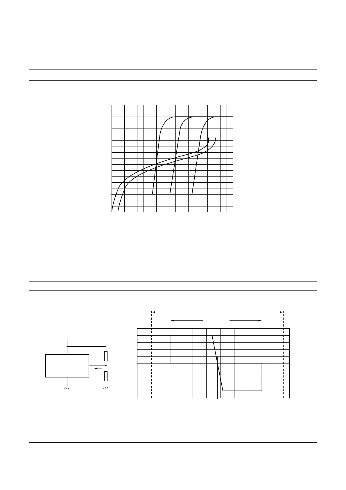
Philips Semiconductors Product specification
I2C-bus controlled multistandard alignment-free
IF-PLL demodulator with FM radio
handbook, full pagewidth
V
SAGC
(V)
4
3
2
1
30 40
50
(3) (4) (5)(2)(1)
60
70 80 90 100 110
V
i(SIF)
MHC149
120
(dBµV)
I
TAGC
(µA)
600
500
400
300
200
100
0
TDA9887
(1) V
(2) V
(3) I
(4) I
(5) I
is SIF-AGC voltage in FM mode.
SAGC
is SIF-AGC voltage in AM mode.
SAGC
is tuner current in TV mode with R
TAGC
is tuner current in TV mode with R
TAGC
is tuner current in TV mode with R
TAGC
V
P
I
AFC
TDA9887
(23)
21
=22kΩ or setting via I2C-bus at −15 dB.
TOP
=10kΩ or setting via I2C-bus at 0 dB.
TOP
=0kΩ or setting via I2C-bus at +15 dB.
TOP
Fig.10 Typical SIF and tuner AGC characteristic.
lock range without SAW filter
AFC window
5
V
AFC
(V)
4
R1
22 kΩ
V
AFC
R2
22 kΩ
3
2
1
0
36 37 38 40 41
38.9
38.71 39.09
f (MHz)
I
AFC
(µA)
−200
−100
0
+100
+200
mhc146
Pin number for TDA9887HN in parenthesis.
Fig.11 Typical analog AFC characteristic for VIF.
2004 Aug 25 41
Page 42
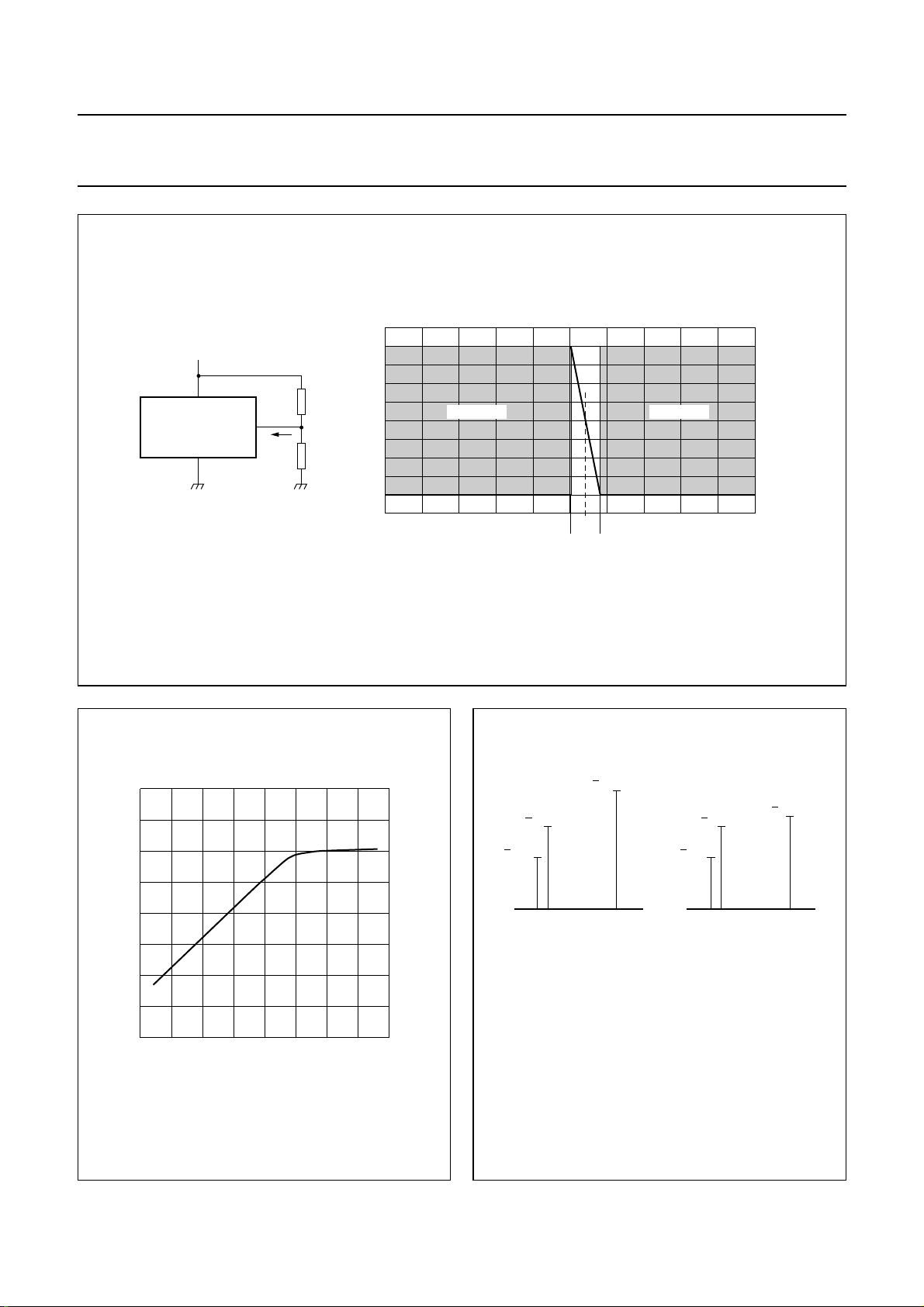
Philips Semiconductors Product specification
I2C-bus controlled multistandard alignment-free
IF-PLL demodulator with FM radio
5
V
R1
22 kΩ
V
AFC
R2
22 kΩ
AFC
(V)
4
3
2
1
0
8 9 10 121110.7 13
not defined not defined
10.5125 10.9125
V
P
TDA9887
21
(23)
I
AFC
TDA9887
f (MHz)
I
AFC
(µA)
−200
−100
0
+100
+200
mhc147
Pin number for TDA9887HN in parenthesis.
Fig.12 Typical analog AFC characteristic for RIF.
V
i(VIF)
mhc112
(dBµV)
80
S/N
(dB)
60
40
20
0
30 50 110
70 90
Fig.13 Typical signal-to-noise ratio as a functionof
VIF input voltage.
3.2 dB
13.2 dB
21 dB
SC CC PC SC CC PC
BLUE YELLOW
SC is sound carrier, with respect to sync level.
CC is chrominance carrier, with respect to sync level.
PC is picture carrier, with respect to sync level.
The sound carrier levels are taking into account a sound shelf
attenuation of 14 dB (SAW filter G1984M).
13.2 dB
21 dB
10 dB
Fig.14 Input signal conditions.
mha739
2004 Aug 25 42
Page 43
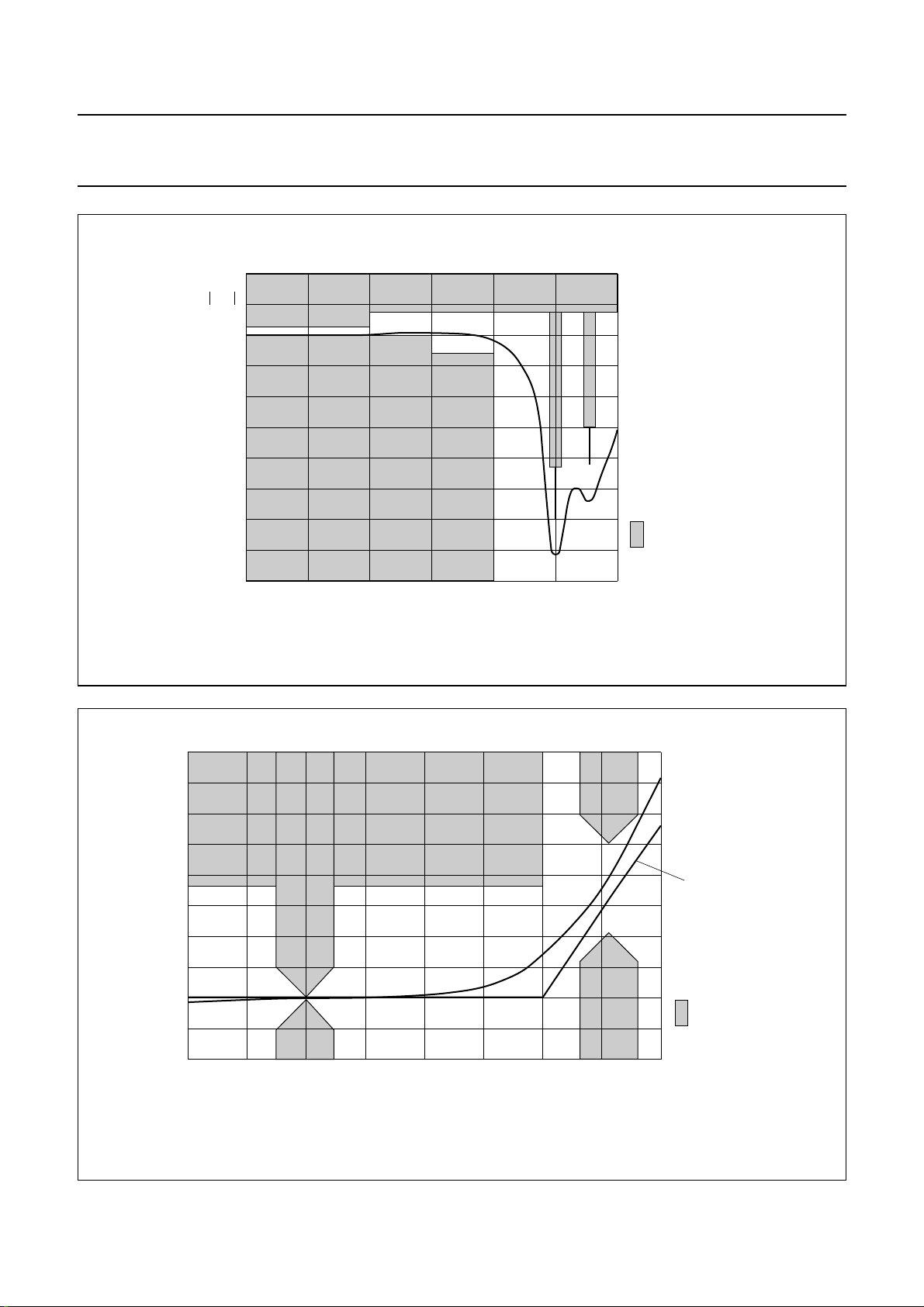
Philips Semiconductors Product specification
I2C-bus controlled multistandard alignment-free
IF-PLL demodulator with FM radio
10
H(s)
(dB)
0
−10
−20
−30
−40
2 2.5 3 3.5 4 4.5 5
TDA9887
mhc122
minimum
requirements
f (MHz)
Fig.15 Typical amplitude response for sound trap at M/N standard (including Korea).
400
group
delay
(ns)
300
200
100
0
−100
0 0.5 1.5 2 31 2.5 3.5 4
mhb167
f (MHz)
ideal characteristic
due to pre-correction
in the transmitter
minimum
requirements
Overall delay is not shown, here the maximum ripple is specified.
Fig.16 Typical group delay for sound trap at M/N standard.
2004 Aug 25 43
Page 44
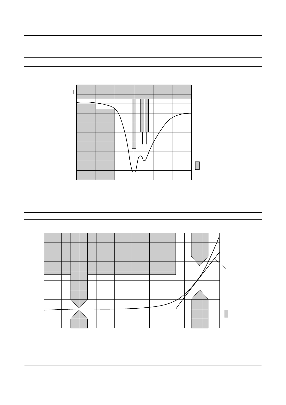
Philips Semiconductors Product specification
I2C-bus controlled multistandard alignment-free
IF-PLL demodulator with FM radio
10
H(s)
(dB)
0
−10
−20
−30
−40
4 4.5 5 5.5 6 6.5 7
TDA9887
mhb168
minimum
requirements
f (MHz)
Fig.17 Typical amplitude response for sound trap at B/G standard.
400
group
delay
(ns)
300
200
100
0
−100
0 0.5 1.5 2 31 2.5 3.5 4 4.5 5
mhb169
ideal characteristic
due to pre-correction
in the transmitter
minimum
requirements
f (MHz)
Overall delay is not shown, here the maximum ripple is specified.
Fig.18 Typical group delay for sound trap at B/G standard.
2004 Aug 25 44
Page 45
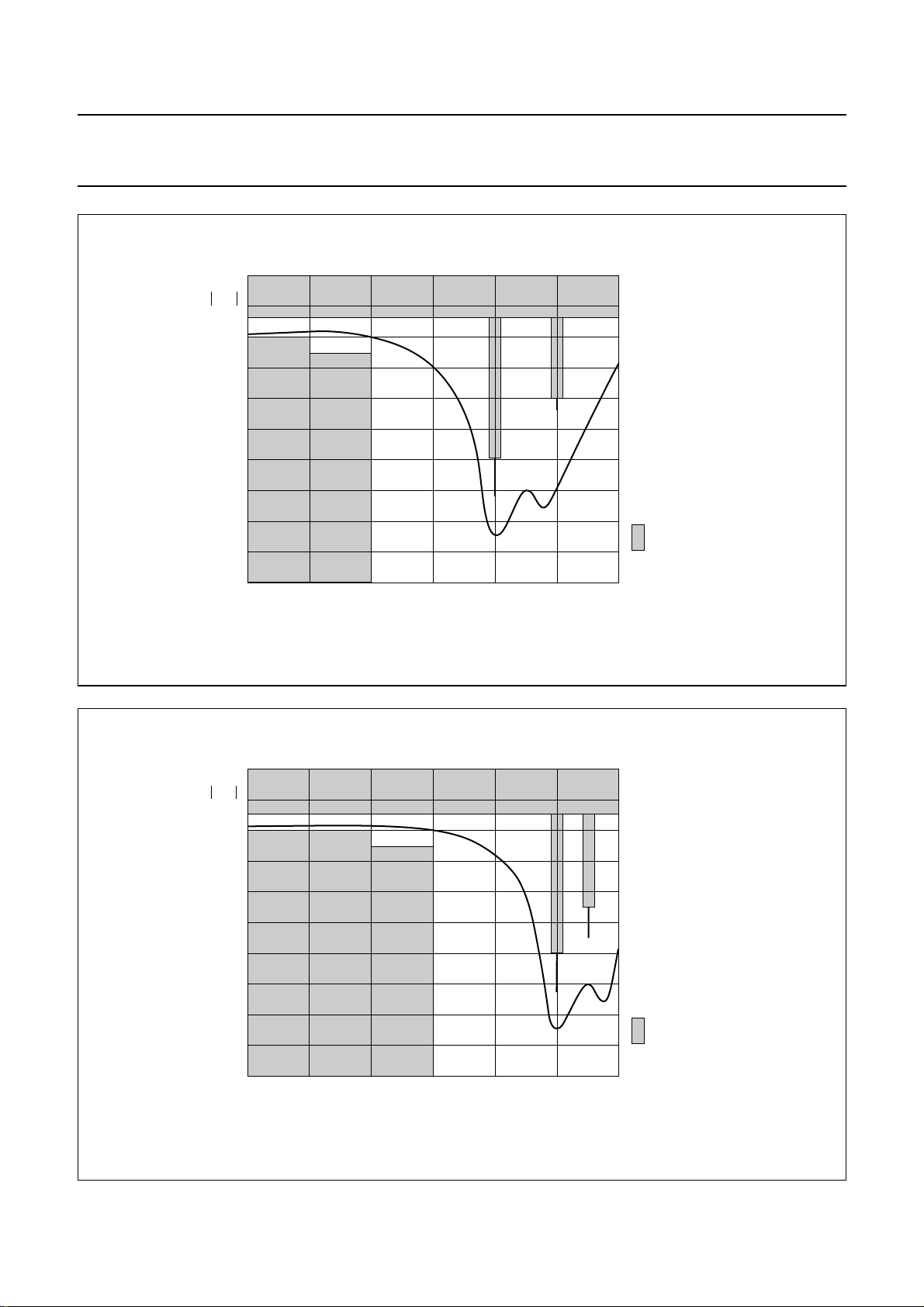
Philips Semiconductors Product specification
I2C-bus controlled multistandard alignment-free
IF-PLL demodulator with FM radio
10
H(s)
(dB)
0
−10
−20
−30
−40
4 4.5 5 5.5 6 6.5 7
TDA9887
mhc123
minimum
requirements
f (MHz)
Fig.19 Typical amplitude response for sound trap at I standard.
10
H(s)
(dB)
0
−10
−20
−30
−40
4 4.5 5 5.5 6 6.5 7
mhb171
minimum
requirements
f (MHz)
Fig.20 Typical amplitude response for sound trap at D/K standard.
2004 Aug 25 45
Page 46
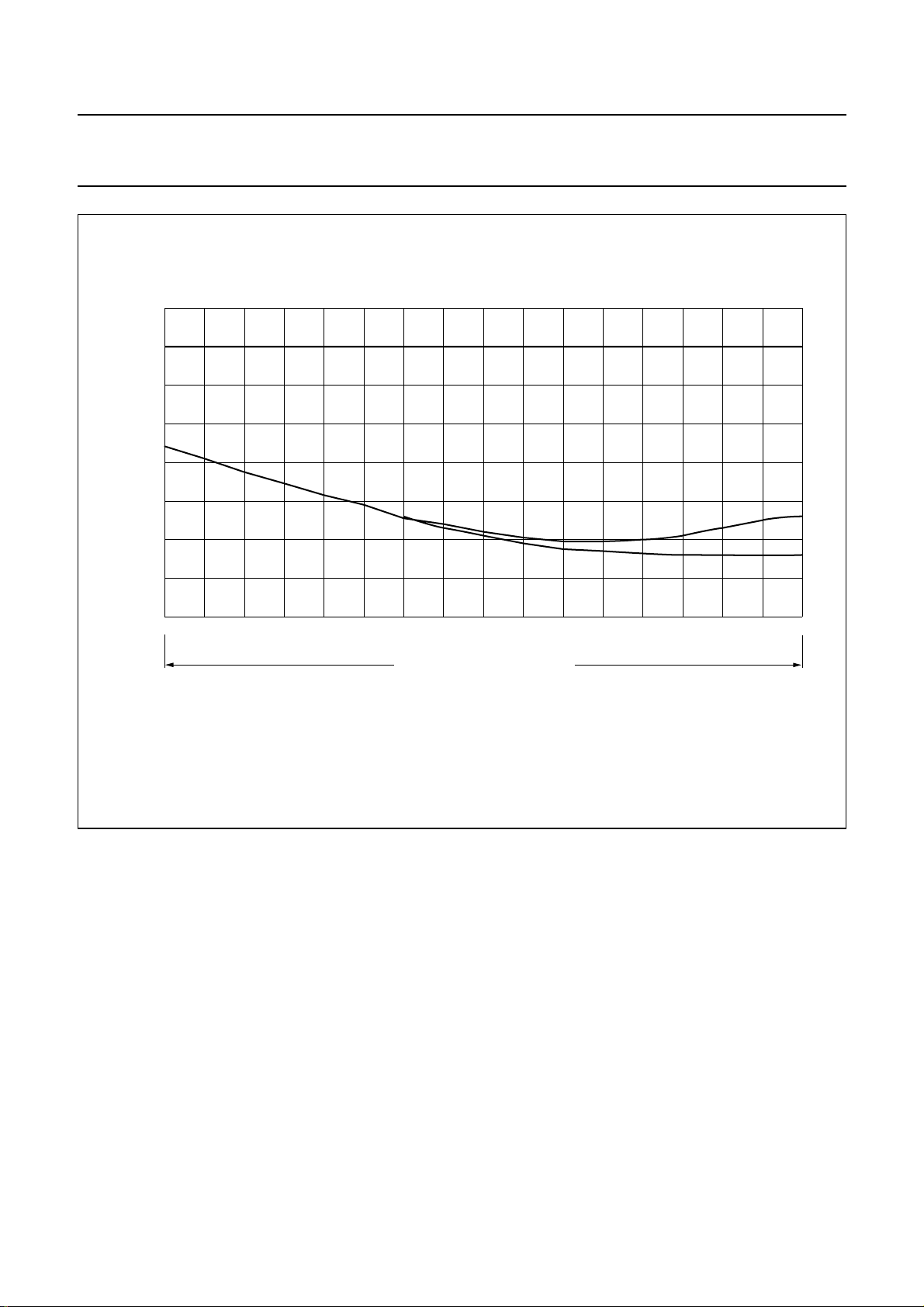
Philips Semiconductors Product specification
I2C-bus controlled multistandard alignment-free
IF-PLL demodulator with FM radio
10
0
S/N
W
(dB)
−10
−20
−30
−40
−50
−60
TDA9887
mhc118
(1)
(2)
(3)
−70
(1) Signal.
(2) Noise at H-picture (CCIR weighted quasi peak).
(3) Noise at black picture (CCIR weighted quasi peak).
4952 46 43 40 1337 10 728 2225 193134 16
gain controlled operation of FM PLL
Conditions: PC/SC ratio measured at pins VIF1 and VIF2; via transformer;
27 kHz FM deviation; 50 µs de-emphasis.
Fig.21 Audio signal-to-noise ratio as a function of picture-to-sound carrier ratio in intercarrier mode.
4
PC/SC ratio
2004 Aug 25 46
Page 47
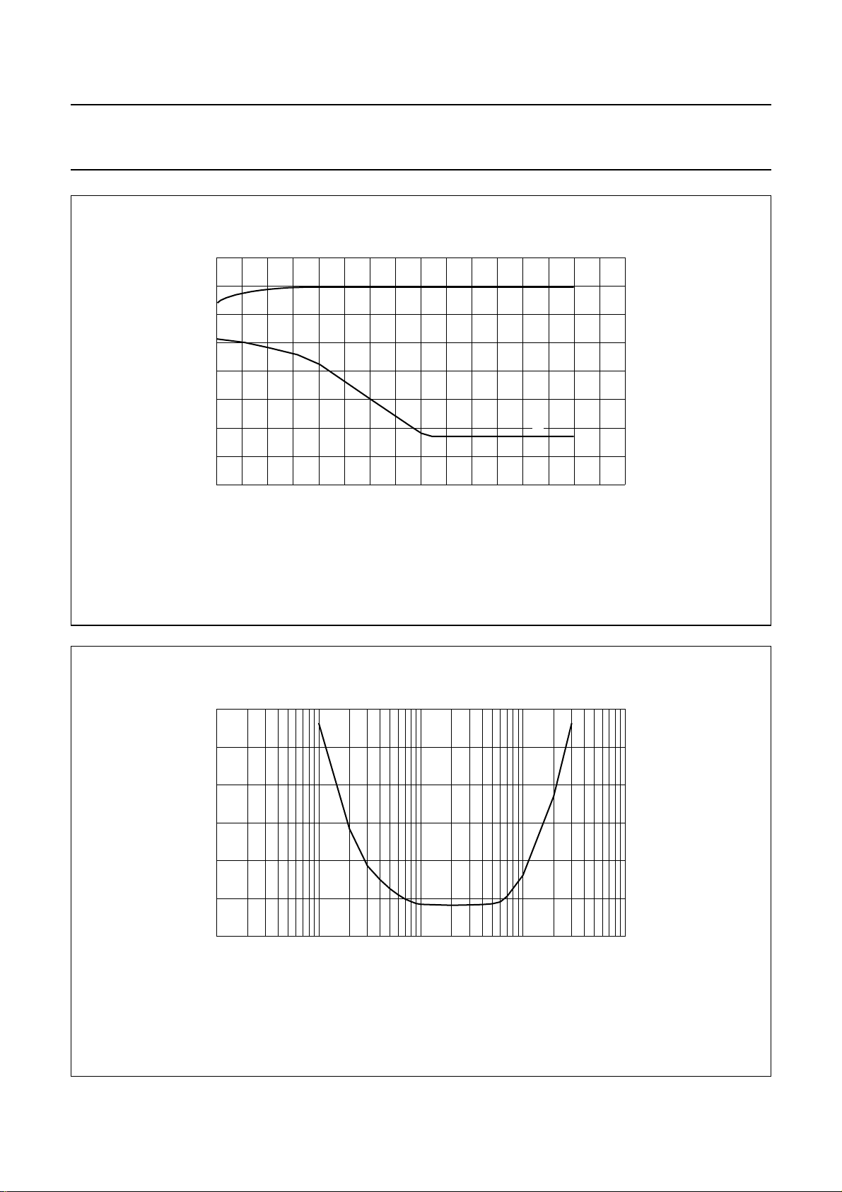
Philips Semiconductors Product specification
I2C-bus controlled multistandard alignment-free
IF-PLL demodulator with FM radio
10
S/N
W
(dB)
−10
−30
−50
−70
30 1109050 70
TDA9887
mhc119
(1)
(2)
Vi (dBµV)
(2) Noise.
Condition: m = 54 %.(1) Signal.
Fig.22 Typical takeover audio signal-to-noise ratio as a function of input signal at AM standard.
fAF (kHz)
mhc120
2
10
THD
(%)
1.5
1.0
0.5
0
−2
10
−1
1
1010
C
= 2.2 µF; m=54%.
AGC
Fig.23 Typical total harmonic distortion as a function of audio frequency at AM standard.
2004 Aug 25 47
Page 48
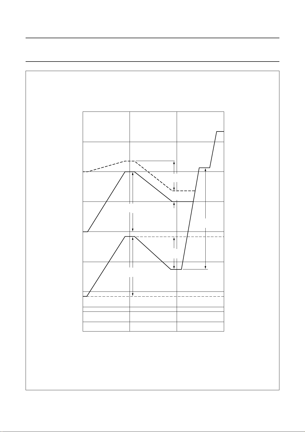
Philips Semiconductors Product specification
I2C-bus controlled multistandard alignment-free
IF-PLL demodulator with FM radio
(dBµV)
140
120
100
(1)
SAW insertion
loss 20 dB
IF slip
80
tuning gain
control range
handbook, full pagewidth
antenna input
6 dB
MHC150
TDA9887
10
IF signals
RMS value
(V)
video 2 V (p-p)
1
−1
10
−2
10
(TOP)
(1) Depends on TOP.
70 dB
VIF AGC
60
SAW insertion
loss 20 dB
40
40 dB
RF gain
20
10
VHF/UHF tuner VIF
tuner SAW filter
VIF amplifier, demodulator
and video
TDA9887
−3
10
0.66 × 10
−4
10
−5
10
0.66 × 10
−3
−5
Fig.24 Front-end level diagram.
2004 Aug 25 48
Page 49
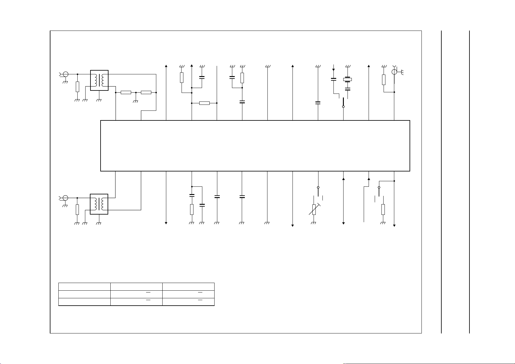
This text is here in white to force landscape pages to be rotated correctly when browsing through the pdf in the Acrobat reader.This text is here in
_white to force landscape pages to be rotated correctly when browsing through the pdf in the Acrobat reader.This text is here inThis text is here in
white to force landscape pages to be rotated correctly when browsing through the pdf in the Acrobat reader. white to force landscape pages to be ...
2004 Aug 25 49
13 TEST AND APPLICATION INFORMATION
Philips Semiconductors Product specification
IF-PLL demodulator with FM radio
I
2
C-bus controlled multistandard alignment-free
SIF
input
VIF
input
51 Ω
51 Ω
1 : 1
1 : 1
(1)
R3
SIF2 SIF1
24
(27)
(30)
1
VIF1 VIF2
(26)
(31)
16
(17)
external
reference
100
pF
470 nF
VAGCAFC VPLL
15
(16)
tuner AGC
4 MHz
C
x
output
14
(15)
51 Ω
TAGC FMINCVBS
radio test
input
13
(14)
AFC
output
22
kΩ
R2
150 kΩ150 kΩ
OP2 REF
23
22
(24)
21
(23)
22 kΩ
100
V
nF
20
(22)
VIF-PLL
(2)
P
filter
1.5
nF
V
P AGND
19
(21)
150 Ω
220 nF
18
(20)
CVBS
output
17
(18)
TDA9887
(1)
2
3
OP1 FMPLL
10 nF
5.6 kΩ
(2)
4
FM-PLL
filter
(3)
5
DEEM AFD DGND AUD
390
pF
(4)
6
10 nF
470 nF
(5)
7
(7)
8
audio
output
22 kΩ
(8)
9
(9)
10
(10)
11
SCL
MAD
select
(11)
12
SIOMADTOP SDA
R1
2.2
kΩ
(1)
intercarrier
output
mhc151
Pin numbers for TDA9887HN in parenthesis.
(1) Optional for I2C-bus address selection.
Option R1 not used R1 = 2.2 kΩ
R2 and R3 not used 1000 011 (R/
R2 = R3 = 150 kΩ 1001 011 (R/W) 1001 010 (R/W)
(2) Different VIF loop filter in comparison with the application circuit due to different input characteristics (SAW filter or transformer).
W) 1000 010 (R/W)
Fig.25 Test circuit.
TDA9887
Page 50
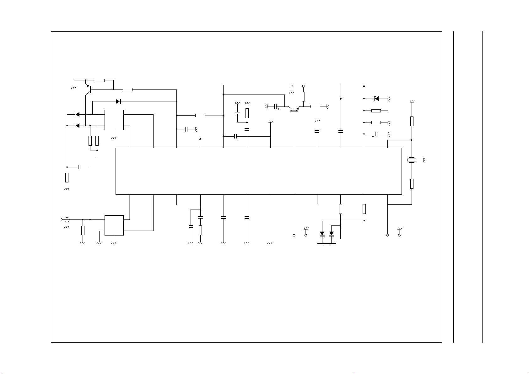
This text is here in white to force landscape pages to be rotated correctly when browsing through the pdf in the Acrobat reader.This text is here in
_white to force landscape pages to be rotated correctly when browsing through the pdf in the Acrobat reader.This text is here inThis text is here in
white to force landscape pages to be rotated correctly when browsing through the pdf in the Acrobat reader. white to force landscape pages to be ...
2004 Aug 25 50
Philips Semiconductors Product specification
IF-PLL demodulator with FM radio
I
2
C-bus controlled multistandard alignment-free
IF
input
BA277
BA277
22 kΩ
10 nF
680 kΩ
220 kΩ
BC847C
6.8
kΩ
5 V
6.8
kΩ
1
2
BA277
SAW
FILTER
K9456
3
5
4
SIF2 SIF1
24
(27)
23
(26)
22
(24)
10 nF
22 kΩ
(1)
21
(23)
5 V
1.5
nF
V
P AGND
20
(22)
10 nF
19
(21)
330 Ω
220 nF
18
(20)
10 µF
CVBS output
BC847
(18)
75 Ω
220 Ω
17
16
(17)
470 nF
VAGCAFC VPLL
f
15
(16)
tuner AGC
ref
(3)
12 kΩ
5 V
100 pF
REF
14
(15)
TAGC FMINCVBSOP2
100 kΩ
47 µF
13
(14)
330 Ω
10.7 MHz
(2)
(2)
TDA9887
(2)
330 Ω
51 Ω
1
2
SAW
FILTER
K3953
3
(30)
1
VIF1 VIF2
5
4
(31)
(1)
2
3
OP1 FMPLL
390
(2)
4
pF
10 nF
5.6 kΩ
(3)
5
(4)
6
DEEM AFD DGND AUD SCL SIOMADTOP SDA
10 nF
470 nF
(5)
7
(7)
8
AF output
(8)
9
(3)
positive supply
2
I
C-bus controller
(9)
10
(10)
11
100 Ω 100 Ω
I2C-bus
(11)
12
intercarrier
output
mhc152
Pin numbers for TDA9887HN in parenthesis.
(1) If pin OP2 outputs VIF-AGC voltage, then pin OP1 can be used for SAW switching.
(2) Only for radio mode, not needed for external FM input mode.
(3) Optional measures to improve ESD performance within a TV-set application.
Fig.26 Application circuit.
TDA9887
Page 51
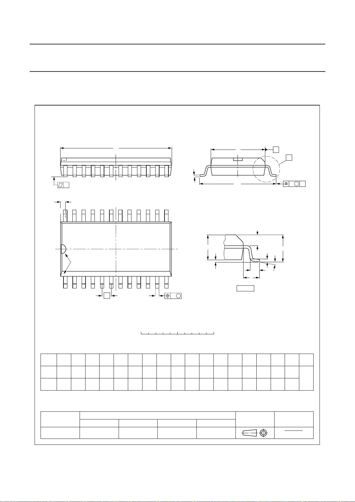
Philips Semiconductors Product specification
I2C-bus controlled multistandard alignment-free
IF-PLL demodulator with FM radio
14 PACKAGE OUTLINES
SO24: plastic small outline package; 24 leads; body width 7.5 mm
D
c
y
Z
24
13
TDA9887
SOT137-1
E
H
E
A
X
v
M
A
pin 1 index
1
e
0 5 10 mm
DIMENSIONS (inch dimensions are derived from the original mm dimensions)
mm
A
max.
2.65
0.1
A1A2A
0.3
2.45
0.1
2.25
0.012
0.096
0.004
0.089
0.25
0.01
b
3
p
0.49
0.32
0.36
0.23
0.019
0.013
0.014
0.009
UNIT
inches
Note
1. Plastic or metal protrusions of 0.15 mm (0.006 inch) maximum per side are not included.
(1)E(1) (1)
cD
15.6
15.2
0.61
0.60
12
w
b
p
M
scale
eHELLpQ
7.6
7.4
0.30
0.29
1.27
0.05
10.65
10.00
0.419
0.394
0.055
1.4
Q
A
2
A
1
detail X
1.1
1.1
1.0
0.4
0.043
0.043
0.039
0.016
0.25
0.01
L
p
L
(A )
0.25 0.1
0.01
A
3
θ
ywv θ
0.004
Z
0.9
0.4
0.035
0.016
o
8
o
0
OUTLINE
VERSION
SOT137-1
IEC JEDEC JEITA
075E05 MS-013
REFERENCES
2004 Aug 25 51
EUROPEAN
PROJECTION
ISSUE DATE
99-12-27
03-02-19
Page 52
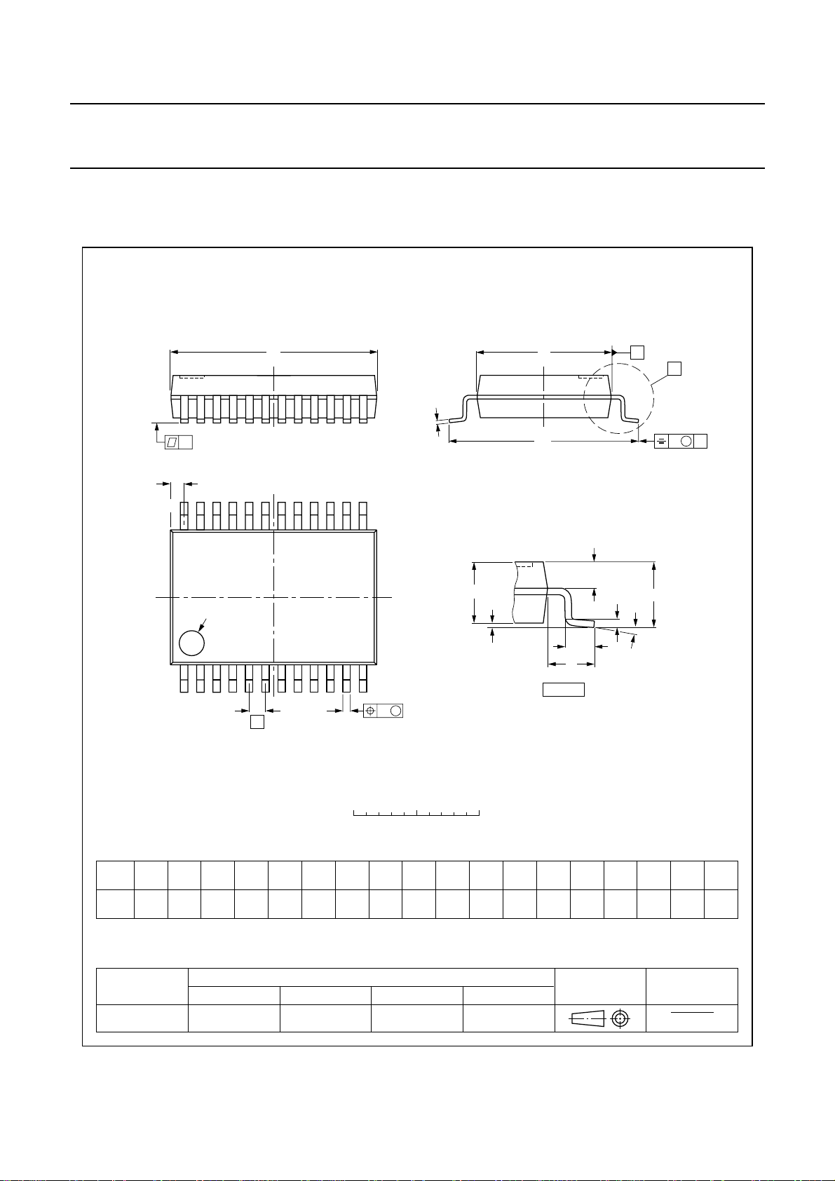
Philips Semiconductors Product specification
I2C-bus controlled multistandard alignment-free
IF-PLL demodulator with FM radio
SSOP24: plastic shrink small outline package; 24 leads; body width 5.3 mm
D
c
y
Z
24 13
TDA9887
SOT340-1
E
H
E
A
X
v
M
A
pin 1 index
112
w
b
e
DIMENSIONS (mm are the original dimensions)
UNIT A1A2A
Note
1. Plastic or metal protrusions of 0.2 mm maximum per side are not included.
A
max.
0.21
mm
2
OUTLINE
VERSION
SOT340-1 MO-150
0.05
1.80
1.65
IEC JEDEC JEITA
0.25
b
3
p
0.38
0.25
p
0 2.5 5 mm
cD
0.20
8.4
0.09
8.0
REFERENCES
M
scale
(1)E(1) (1)
5.4
0.65 1.25
5.2
Q
A
2
A
1
detail X
eHELLpQZywv θ
7.9
7.6
1.03
0.63
0.9
0.7
(A )
L
p
L
EUROPEAN
PROJECTION
A
3
θ
0.13 0.10.2
0.8
0.4
ISSUE DATE
99-12-27
03-02-19
o
8
o
0
2004 Aug 25 52
Page 53
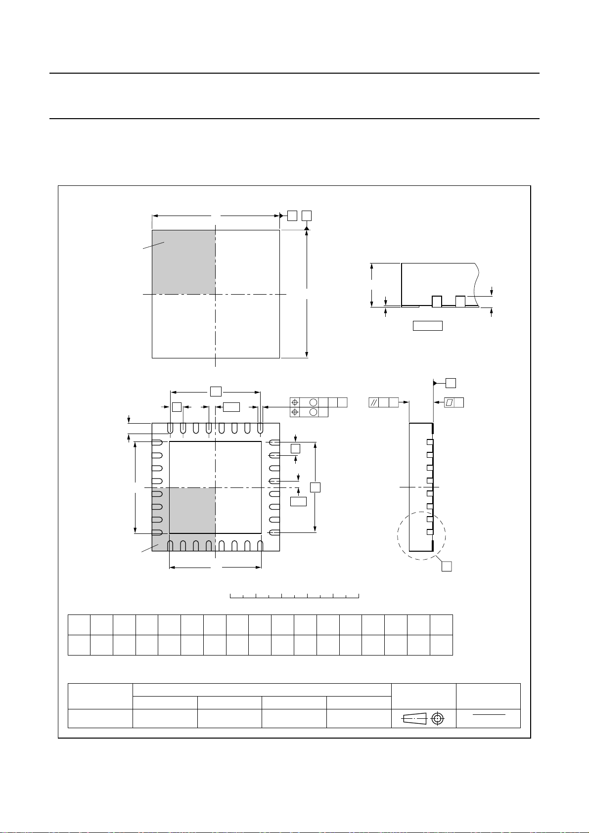
Philips Semiconductors Product specification
I2C-bus controlled multistandard alignment-free
IF-PLL demodulator with FM radio
HVQFN32: plastic thermal enhanced very thin quad flat package; no leads;
32 terminals; body 5 x 5 x 0.85 mm
A
D
terminal 1
index area
B
A
E
TDA9887
SOT617-3
A
1
detail X
c
e
1
e
916
L
8
E
h
1
terminal 1
index area
DIMENSIONS (mm are the original dimensions)
(1)
A
UNIT
mm
Note
1. Plastic or metal protrusions of 0.075 mm maximum per side are not included.
OUTLINE
VERSION
SOT617-3 MO-220- - - - - -
max.
A
0.05
0.00
1
32 25
(1)
c
b
0.30
0.18
D
5.1
0.2
4.9
IEC JEDEC JEITA
1/2
e
b
17
e
1/2
24
D
h
0 2.5 5 mm
scale
(1)
D
3.75
3.45
h
E
E
h
5.1
3.75
4.9
3.45
REFERENCES
0.51
e
3.5
C
v
M
ACCB
w
M
e
2
e
e
3.5
L
2
0.5
0.3
1
y
C
1
w
0.1v0.05
ye
0.05 0.1
EUROPEAN
PROJECTION
y
X
y
1
ISSUE DATE
02-04-18
02-10-22
2004 Aug 25 53
Page 54

Philips Semiconductors Product specification
I2C-bus controlled multistandard alignment-free
IF-PLL demodulator with FM radio
15 SOLDERING
15.1 Introduction to soldering surface mount packages
Thistextgives a very brief insighttoacomplex technology.
A more in-depth account of soldering ICs can be found in
our
“Data Handbook IC26; Integrated Circuit Packages”
(document order number 9398 652 90011).
There is no soldering method that is ideal for all surface
mount IC packages. Wave soldering can still be used for
certainsurfacemount ICs, but it is notsuitableforfinepitch
SMDs. In these situations reflow soldering is
recommended.
15.2 Reflow soldering
Reflow soldering requires solder paste (a suspension of
fine solder particles, flux and binding agent) to be applied
tothe printed-circuit board byscreenprinting, stencilling or
pressure-syringe dispensing before package placement.
Driven by legislation and environmental forces the
worldwide use of lead-free solder pastes is increasing.
Several methods exist for reflowing; for example,
convection or convection/infrared heating in a conveyor
type oven. Throughput times (preheating, soldering and
cooling) vary between 100 seconds and 200 seconds
depending on heating method.
Typical reflow peak temperatures range from
215 °C to 270 °C depending on solderpaste material. The
top-surface temperature of the packages should
preferably be kept:
• below 225 °C (SnPb process) or below 245 °C (Pb-free
process)
– for all BGA, HTSSON-T and SSOP-T packages
– for packages with a thickness ≥ 2.5 mm
– for packages with a thickness < 2.5 mm and a
volume ≥ 350 mm3 so called thick/large packages.
• below 240 °C (SnPb process) or below 260 °C (Pb-free
process) for packages with a thickness < 2.5 mm and a
volume < 350 mm3 so called small/thin packages.
Moisture sensitivity precautions, as indicated on packing,
must be respected at all times.
To overcome these problems the double-wave soldering
method was specifically developed.
If wave soldering is used the following conditions must be
observed for optimal results:
• Use a double-wave soldering method comprising a
turbulent wave with high upward pressure followed by a
smooth laminar wave.
• For packages with leads on two sides and a pitch (e):
– larger than or equal to 1.27 mm, the footprint
longitudinal axis is preferred to be parallel to the
transport direction of the printed-circuit board;
– smaller than 1.27 mm, the footprint longitudinal axis
must be parallel to the transport direction of the
printed-circuit board.
The footprint must incorporate solder thieves at the
downstream end.
• Forpackageswith leads on four sides, thefootprintmust
be placed at a 45° angle to the transport direction of the
printed-circuit board. The footprint must incorporate
solder thieves downstream and at the side corners.
During placement andbefore soldering, the package must
be fixed with a droplet of adhesive. The adhesive can be
applied by screen printing, pin transfer or syringe
dispensing. The package can be soldered after the
adhesive is cured.
Typical dwell time of the leads in the wave ranges from
3 seconds to 4 seconds at 250 °C or 265 °C, depending
on solder material applied, SnPb or Pb-free respectively.
A mildly-activated flux will eliminate the need for removal
of corrosive residues in most applications.
15.4 Manual soldering
Fix the component by first soldering two
diagonally-opposite end leads. Use a low voltage (24 V or
less) soldering iron applied to the flat part of the lead.
Contact time must be limited to 10 seconds at up to
300 °C.
When using a dedicated tool, all other leads can be
soldered in one operation within 2 seconds to 5 seconds
between 270 °C and 320 °C.
TDA9887
15.3 Wave soldering
Conventional single wave soldering is not recommended
forsurfacemount devices (SMDs) or printed-circuit boards
with a high component density, as solder bridging and
non-wetting can present major problems.
2004 Aug 25 54
Page 55

Philips Semiconductors Product specification
I2C-bus controlled multistandard alignment-free
TDA9887
IF-PLL demodulator with FM radio
15.5 Suitability of surface mount IC packages for wave and reflow soldering methods
(1)
(3)
, TFBGA,
not suitable suitable
BGA, HTSSON..T
PACKAGE
(3)
, LBGA, LFBGA, SQFP, SSOP..T
USON, VFBGA
DHVQFN, HBCC, HBGA, HLQFP, HSO, HSOP, HSQFP, HSSON,
not suitable
HTQFP, HTSSOP, HVQFN, HVSON, SMS
(5)
PLCC
, SO, SOJ suitable suitable
LQFP, QFP, TQFP not recommended
SSOP, TSSOP, VSO, VSSOP not recommended
CWQCCN..L
(8)
, PMFP
(9)
, WQCCN..L
(8)
not suitable not suitable
Notes
1. Formoredetailed information on the BGApackages refer to the
“(LF)BGAApplication Note
from your Philips Semiconductors sales office.
2. All surface mount (SMD) packages are moisture sensitive. Depending upon the moisture content, the maximum
temperature (with respect to time) and body size of the package, there is a risk that internal or external package
cracks may occur due to vaporization of the moisture in them (the so called popcorn effect). For details, refer to the
Drypack information in the
“Data Handbook IC26; Integrated Circuit Packages; Section: Packing Methods”
3. These transparent plastic packages are extremely sensitive to reflow soldering conditions and must on no account
be processed through more than one soldering cycle or subjectedto infrared reflow soldering with peak temperature
exceeding 217 °C ± 10 °C measured in the atmosphere of the reflow oven. The package body peak temperature
must be kept as low as possible.
4. These packages are not suitable for wave soldering. On versions with the heatsink on the bottom side, the solder
cannot penetrate between the printed-circuit board and the heatsink. On versions with the heatsink on the top side,
the solder might be deposited on the heatsink surface.
5. If wave soldering is considered, then the package must be placed at a 45° angle to the solder wave direction.
The package footprint must incorporate solder thieves downstream and at the side corners.
6. Wavesoldering is suitable for LQFP, TQFP and QFP packages with a pitch (e) larger than 0.8 mm; it is definitely not
suitable for packages with a pitch (e) equal to or smaller than 0.65 mm.
7. Wave soldering is suitable for SSOP, TSSOP, VSO and VSSOP packages with a pitch (e) equal to or larger than
0.65 mm; it is definitely not suitable for packages with a pitch (e) equal to or smaller than 0.5 mm.
8. Image sensor packages in principle should not be soldered. They are mounted in sockets or delivered pre-mounted
on flex foil. However, the image sensor package can be mounted by the client on a flex foil by using a hot bar
soldering process. The appropriate soldering profile can be provided on request.
9. Hot bar or manual soldering is suitable for PMFP packages.
SOLDERING METHOD
WAVE REFLOW
(4)
(5)(6)
(7)
suitable
suitable
suitable
”(AN01026); order a copy
(2)
.
2004 Aug 25 55
Page 56

Philips Semiconductors Product specification
I2C-bus controlled multistandard alignment-free
TDA9887
IF-PLL demodulator with FM radio
16 DATA SHEET STATUS
LEVEL
I Objective data Development This data sheet contains data from the objective specification for product
II Preliminary data Qualification This data sheet contains data from the preliminary specification.
III Product data Production This data sheet contains data from the product specification. Philips
Notes
1. Please consult the most recently issued data sheet before initiating or completing a design.
2. The product status of the device(s) described in this data sheet may have changed since this data sheet was
3. Fordata sheets describing multiple type numbers, the highest-level product status determinesthe data sheet status.
DATA SHEET
STATUS
published. The latest information is available on the Internet at URL http://www.semiconductors.philips.com.
(1)
PRODUCT
STATUS
(2)(3)
DEFINITION
development. Philips Semiconductors reserves the right to change the
specification in any manner without notice.
Supplementary data will be published at a later date. Philips
Semiconductors reserves the right to change the specification without
notice, in order to improve the design and supply the best possible
product.
Semiconductors reserves the right to make changes at any time in order
to improve the design, manufacturing and supply. Relevant changes will
be communicated via a Customer Product/Process Change Notification
(CPCN).
17 DEFINITIONS Short-form specification The data in a short-form
specification is extracted from a full data sheet with the
same type number and title. For detailed information see
the relevant data sheet or data handbook.
Limiting values definition Limiting values given are in
accordance with the Absolute Maximum Rating System
(IEC 60134). Stress above one or more of the limiting
values may cause permanent damage to the device.
These are stress ratings only and operation of the device
atthese or at any otherconditionsabovethose given in the
Characteristics sections of the specification is not implied.
Exposure to limiting values for extended periods may
affect device reliability.
Application information Applications that are
described herein for any of these products are for
illustrative purposes only. Philips Semiconductors make
norepresentationorwarranty that such applications will be
suitable for the specified use without further testing or
modification.
18 DISCLAIMERS Life support applications These products are not
designed for use in life support appliances, devices, or
systems where malfunction of these products can
reasonably be expected to result in personal injury. Philips
Semiconductorscustomersusingorselling these products
for use in such applications do so at their own risk and
agree to fully indemnify Philips Semiconductors for any
damages resulting from such application.
Right to make changes Philips Semiconductors
reserves the right to make changes in the products including circuits, standard cells, and/or software described or contained herein in order to improve design
and/or performance. Whenthe product is in fullproduction
(status ‘Production’), relevant changes will be
communicated via a Customer Product/Process Change
Notification (CPCN). Philips Semiconductors assumes no
responsibility or liability for the use of any of these
products, conveys no licence or title under any patent,
copyright, or mask work right to these products, and
makes no representations or warranties that these
products are free from patent, copyright, or mask work
right infringement, unless otherwise specified.
2004 Aug 25 56
Page 57

Philips Semiconductors Product specification
I2C-bus controlled multistandard alignment-free
IF-PLL demodulator with FM radio
19 PURCHASE OF PHILIPS I2C COMPONENTS
Purchase of Philips I2C components conveys a license under the Philips’ I2C patent to use the
components in the I2C system provided the system conforms to the I2C specification defined by
Philips. This specification can be ordered using the code 9398 393 40011.
TDA9887
2004 Aug 25 57
Page 58

Philips Semiconductors – a w orldwide compan y
Contact information
For additional information please visit http://www.semiconductors.philips.com. Fax: +31 40 27 24825
For sales offices addresses send e-mail to: [email protected].
© Koninklijke Philips Electronics N.V. 2004
All rights are reserved. Reproduction in whole or in part is prohibited without the prior written consent of the copyright owner.
The information presented in this document does not form part of any quotation or contract, is believed to be accurate and reliable and may be changed
without notice. No liability will be accepted by the publisher for any consequence of its use. Publication thereof does not convey nor imply any license
under patent- or other industrial or intellectual property rights.
Printed in The Netherlands R25/03/pp58 Date of release: 2004 Aug 25 Document order number: 9397 750 13539
SCA76
 Loading...