

INTEGRATED CIRCUITS
DATA SH EET
TDA9853H
2
I
C-bus controlled economic BTSC
stereo decoder and audio
processor
Product specification
File under Integrated Circuits, IC02
2000 Dec 11

Philips Semiconductors Product specification
I2C-bus controlled economic BTSC stereo
decoder and audio processor
FEATURES
• Voltage Controlled Amplifier (VCA) noise reduction
circuit
• Stereo or mono selectable at the AF outputs
• Stereo pilot PLL circuit with ceramic resonator
• Automatic pilot cancellation
• I2C-bus transceiver.
Audio processor
• Selector for internal and external signals (line in)
• Automatic Volume Level (AVL) control
(control range +6 to −15 dB)
• Volume control (control range +12 to −63 dB)
• Mute control via I2C-bus
• 4 fixed tone settings.
ORDERING INFORMATION
GENERAL DESCRIPTION
The TDA9853H is a bipolar-integrated BTSC stereo
decoder and audio processor for application in TV sets,
VCRs and multimedia PCs.
TDA9853H
TYPE
NUMBER
TDA9853H QFP44 plastic quad flat package; 44 leads (lead length 2.35 mm); body 14 × 14 × 2.2 mm SOT205-1
NAME DESCRIPTION VERSION
PACKAGE
2000 Dec 11 2
Philips Semiconductors Product specification
I2C-bus controlled economic BTSC stereo
TDA9853H
decoder and audio processor
QUICK REFERENCE DATA
SYMBOL PARAMETER CONDITIONS MIN. TYP. MAX. UNIT
V
CC
I
CC
V
o(rms)
α
csL,R
THD
S/N signal-to-noise ratioat line out
V
I, O(rms)
AVL AVL control range −15 − +6 dB
G
c
L
linear
L
bass(max)
L
bass(min)
L
treble(max)
L
treble(min)
supply voltage 7.8 8 9 V
supply current 25 33 45 mA
output voltage (RMS value) composite input voltage 250 mV (RMS)
− 500 − mV
for 100% modulation L + R
stereo channel separation
(25 kHz deviation); f
14% modulation; fL= 300 Hz; fR= 3 kHz 15 20 − dB
mod
= 300 Hz
L and R
total harmonic distortion
L,R
100% modulation L or R; f
= 1 kHz − 0.2 1 %
mod
L and R
2
C-bus; referenced to 500 mV
and at AF output
mono via I
output signal; volume 0 dB
CCIR 468-2 weighted; quasi peak 50 60 − dB
DIN noise weighting filter (RMS value) − 73 − dBA
signal handling (RMS value) THD < 0.5% 2 −−V
volume control range −63 − +12 dB
linear tone control − 0 − dB
tone control with maximum
bass
tone control with minimum
bass
tone control with maximum
treble
tone control with minimum
treble
referenced to linear position;
f
=20Hz
mod
referenced to linear position;
f
=20Hz
mod
referenced to linear position;
f
=20kHz
mod
referenced to linear position;
f
=20kHz
mod
10 12 − dB
3.5 5 − dB
68−dB
−−1.5 − dB
2000 Dec 11 3
This text is here in white to force landscape pages to be rotated correctly when browsing through the pdf in the Acrobat reader.This text is here in
_white to force landscape pages to be rotated correctly when browsing through the pdf in the Acrobat reader.This text is here inThis text is here in
white to force landscape pages to be rotated correctly when browsing through the pdf in the Acrobat reader. white to force landscape pages to be ...
2000 Dec 11 4
C3
C2
R1
C4
Q1
C6C5
handbook, full pagewidth
External Input Right
(EIR)
C7
C8
C9
C10
C11
C12
BLOCK DIAGRAM
Philips Semiconductors Product specification
decoder and audio processor
I
2
C-bus controlled economic BTSC stereo
composite
baseband
input
C1
COMP
R2
FDO
R3
FDI
CP2CP1C
342
4
STEREO DECODER
35
33
DETECTOR
VOLTAGE CONTROLLED
AND
AMPLIFIER
32
BPU
C22C23
C
AV
29
AUTOMATIC
VOLUME
AND
LEVEL CONTROL
I2C-BUS
TRANSCEIVER
MAD
SCL SDA
DGND
VAR VIR
37383940
11
VAL VIL
VOLUME
RIGHT
CONTROL
VOLUME
LEFT
CONTROL
C16
TC1R21TC2R
2423
TONE
RIGHT
CONTROL
TONE
LEFT
CONTROL
10
TC1L13TC2L
C15
BCR
19
20
18
16
14
15
BCL
C14
C13
OUTR
OUTL
MHB789
41
V
CC
C
MO
5
DEMATRIX
MODE SELECT
SUPPLY
28
V
CAP
C19
CER
PH
432
L + R
L − R
31
C
W
C21
30
TW
C20
AND
C
6
AGND36V
LOR
SS
25
27
9
LOL
ref
External Input Left
(EIL)
LIR
26
INPUT
SELECT
FILTER
AND
REFERENCE
8
LIL
C17C18
TDA9853H
7
R
FR
R4
TDA9853H
Fig.1 Block diagram.
Philips Semiconductors Product specification
I2C-bus controlled economic BTSC stereo
TDA9853H
decoder and audio processor
Component list
Electrolytic capacitors ±20%; foil capacitors ±10%; resistors ±5%; unless otherwise specified; see Fig.1.
COMPONENT VALUE TYPE REMARK
C1 2.2 µF electrolytic 63 V
C2 220 nF foil
C3 2.2 µF electrolytic 63 V
C4 220 nF foil
C5 2.2 µF electrolytic 63 V
C6 2.2 µF electrolytic 63 V
C7 2.2 µF electrolytic 63 V
C8 4.7 µF electrolytic 63 V ±10%
C9 2.2 µF electrolytic 63 V
C10 3.3 nF foil
C11 150 pF foil
C12 56 nF foil
C13 56 nF foil
C14 150 pF foil
C15 3.3 nF foil
C16 2.2 µF electrolytic 63 V
C17 2.2 µF electrolytic 63 V
C18 100 µF electrolytic 16 V
C19 100 µF electrolytic 16 V
C20 10 µF electrolytic 63 V
C21 1 µF electrolytic 63 V
C22 4.7 nF foil
C23 22 nF foil
R1 3.3 kΩ
R2 15 kΩ
R3 1.3 kΩ
R4 100 kΩ
Q1 CSB503F58 radial leads
CSB503JF958 alternative as SMD
2000 Dec 11 5
Philips Semiconductors Product specification
I2C-bus controlled economic BTSC stereo
decoder and audio processor
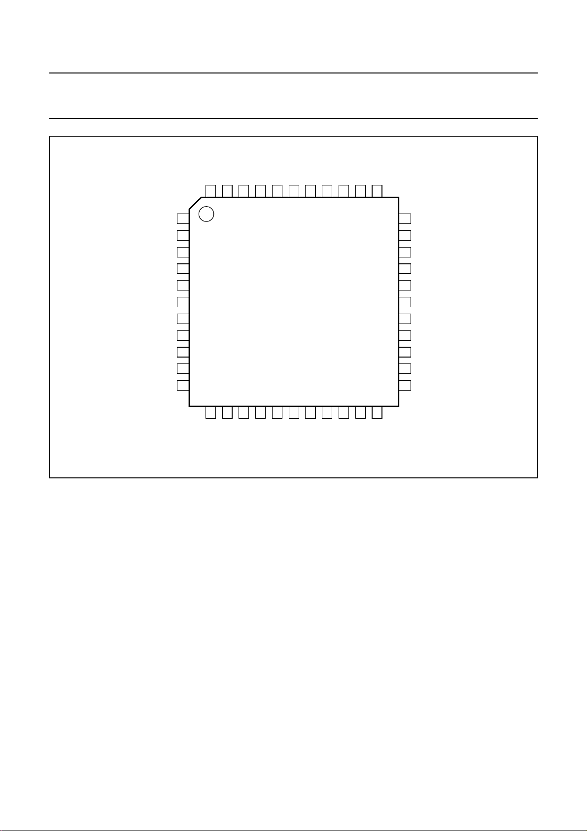
PINNING
SYMBOL PIN DESCRIPTION
n.c. 1 not connected
C
P2
C
P1
COMP 4 composite input signal
C
MO
C
SS
R
FR
LIL 8 line input; left channel
LOL 9 line output; left channel
VIL 10 volume control input; left channel
VAL 11 AVL output; left channel
n.c. 12 not connected
TC1L 13 treble capacitor 1; left channel
TC2L 14 treble capacitor 2; left channel
BCL 15 bass capacitor; left channel
OUTL 16 left channel output
n.c. 17 not connected
OUTR 18 right channel output
BCR 19 bass capacitor; right channel
TC2R 20 treble capacitor 2; right channel
TC1R 21 treble capacitor 1; right channel
n.c. 22 not connected
VAR 23 AVL output; right channel
2 connector 2 for pilot detector capacitor
3 connector 1 for pilot detector capacitor
5 capacitor for DC-decoupling mono
6 capacitor for DC-decoupling stereo
7 resistor for filter reference
TDA9853H
SYMBOL PIN DESCRIPTION
VIR 24 volume control input; right channel
LOR 25 line output; right channel
LIR 26 line input; right channel
V
ref
V
CAP
C
AV
TW 30 capacitor timing
C
W
BPU 32 band-pass filter upper corner
FDO 33 fixed de-emphasis output
n.c. 34 not connected
FDI 35 fixed de-emphasis input
AGND 36 analog ground
DGND 37 digital ground
SDA 38 serial data input/output
MAD 39 programmable address bit
SCL 40 serial clock input
V
CC
C
PH
CER 43 ceramic resonator
n.c. 44 not connected
27 reference voltage (0.5VCC)
28 capacitor for electronic filtering of
supply
29 capacitor for AVL
31 capacitor for VCA and band-pass filter
lower corner frequency
frequency
(module address)
41 supply voltage
42 capacitor for phase detector
2000 Dec 11 6
Philips Semiconductors Product specification
I2C-bus controlled economic BTSC stereo
decoder and audio processor
n.c.
CER
handbook, full pagewidth
n.c.
C
P2
C
P1
COMP
C
MO
C
SS
R
FR
LIL
LOL
VIL
VAL
44
1
2
3
4
5
6
7
8
9
10
11
CPHVCCSCL
43
42
41
40
TDA9853H
MAD
39
SDA
38
DGND
37
AGND
36
FDI
35
n.c.
34
TDA9853H
33
FDO
32
BPU
31
C
W
30
TW
29
C
AV
28
V
CAP
27
V
ref
26
LIR
25
LOR
24
VIR
23
VAR
12
13
14
15
n.c.
TC1L
TC2L
BCL
Fig.2 Pin configuration.
FUNCTIONAL DESCRIPTION
Stereo decoder
The composite signal is fed into a pilot detector/pilot
cancellation circuit and into the MPX demodulator. The
main L + R signal passes a 75 µs fixed de-emphasis filter
andisfedinto the dematrix circuit. Thedecodedsub-signal
L − R is applied to the Volume Controlled Amplifier (VCA)
circuit. To generatethe pilot signalthe stereo demodulator
uses a PLL circuit including a ceramic resonator.
Mode selection
The L − R signal is fed via the internal VCA circuit to the
dematrix/switching circuit. Mode selection is achieved via
the I2C-bus (see Table 9).
The dematrix outputs can be muted via the I2C-bus
(see Table 14).
16
17
18
19
20
21
22
MHB790
OUTL
n.c.
OUTR
BCR
TC2R
TC1R
n.c.
Automatic volume level control
The automatic volume level stage controls its output
voltage to a constant level of typically 200 mV (RMS) from
an input voltage range between 0.1 to 1.1 V (RMS). The
circuitadjustsvariationsinmodulationduringbroadcasting
and because of changes in the programme material; this
functioncan be switchedoff. To avoid audibleplops during
the permanent operation of the AVL circuit a soft blending
scheme has been applied between the different gain
stages. A capacitor (4.7 µF) at pin CAV determines the
attack and decay time constants. In addition the ratio of
attack and decay times can be changed via the I2C-bus.
Integrated filters
The filter functions necessary for stereo demodulation are
provided on-chip using transconductor circuits. The filter
frequencies are controlled bythe filter reference circuit via
the external resistor R4.
2000 Dec 11 7
Philips Semiconductors Product specification
I2C-bus controlled economic BTSC stereo
decoder and audio processor
Audio processor
SELECTOR
Theselectorenablesthe selection of either theinternalline
output signals LOR and LOL (dematrix output) or the
external line input signals LIR and LIL (see Table 16). The
input signal capability of the line inputs (LIR/LIL) is
2 V (RMS). The output of the selector is DC-coupled to the
automatic volume level control circuit.
VOLUME
The volume control range is from +12 dB to −63 dB in
steps of 1 dB and ends with a mute step (see Table 8).
Balance control is achieved by the independent volume
control of each channel.
BASS FUNCTION
A single external 56 nF capacitor for each channel in
combinationwith a linearoperational amplifier andinternal
resistors provides a bass range of +12 dB for high bass
and +5 dB for low bass.
TDA9853H
TREBLE FUNCTION
Two external capacitors C15 = 3.3 nF and C14 = 150 pF
for each channel in combination with a linear operational
amplifier and internal resistors provide a treble range of
+8 dB for high treble and −1.5 dB for low treble.
MUTE
The mute functioncan be activatedindependently with the
last step of volume control at the left or right output. By
setting the general mute bit GMU the audio outputs OUTL
and OUTR are muted.
LIMITING VALUES
In accordance with the Absolute Maximum Rating System (IEC 60134).
SYMBOL PARAMETER CONDITIONS MIN. MAX. UNIT
V
CC
V
SDA, VSCL
V
n
T
amb
T
stg
V
es
supply voltage − 9.5 V
voltage at pins SDA and SCL referenced
to GND
voltage of all other pins to GND 0 V
VCC≤ 9V −0.3 +V
V
>9V −0.3 +9 V
CC
CC
CC
V
V
ambient temperature −20 +70 °C
storage temperature −65 +150 °C
electrostatic handling voltage note 1 −200 +200 V
note 2 −2000 +2000 V
Notes
1. Machine model class B, equivalent to discharging a 200 pF capacitor through a 0 Ω series resistor (‘0 Ω’ is actually
0.75 µH+10Ω).
2. Human body model class B, equivalent to discharging a 100 pF capacitor through a 1500 Ω series resistor.
THERMAL CHARACTERISTICS
SYMBOL PARAMETER CONDITIONS VALUE UNIT
R
th(j-a)
thermal resistance from junction to ambient in free air 70 K/W
2000 Dec 11 8
Philips Semiconductors Product specification
I2C-bus controlled economic BTSC stereo
TDA9853H
decoder and audio processor
CHARACTERISTICS
All voltages are measured relative to GND; VCC=8V; Rs= 600 Ω; AC-coupled; RL=10kΩ; CL= 2.5 nF; f
mono signal; composite input voltage 250 mV (RMS) for 100% modulation L + R (25 kHz deviation); pilot 50 mV (RMS);
Gv= 0 dB; linear tone control; AVL off; T
=25°C; see Fig.1; unless otherwise specified.
amb
SYMBOL PARAMETER CONDITIONS MIN. TYP. MAX. UNIT
Supplies
V
CC
I
CC
V
ref
supply voltage 7.8 8 9 V
supply current 25 33 45 mA
internal reference voltage at
pin V
ref
0.45VCC0.5V
CC
0.55VCCV
Input stage
V
i(max)(rms)
maximum input voltage
2 −−V
(RMS value)
Z
i
input impedance 20 25 32 kΩ
Stereo decoder
HR headroom for L + R, L and R f
V
pil(rms)
nominal stereo pilot voltage
= 300 Hz; THD < 15% 9 −−dB
mod
− 50 − mV
(RMS value)
V
th(on)(rms)
pilot threshold voltage, stereo
−− 35 mV
on (RMS value)
V
th(off)(rms)
pilot threshold voltage, stereo
15 −−mV
off (RMS value)
hys hysteresis − 2.5 − dB
V
o(rms)
α
cs(L,R)
THD
L,R
S/N signal-to-noise ratio at line
output voltage (RMS value) 100% modulation L + R;
f
= 300 Hz
mod
stereo channel separation
L and R
total harmonic distortion
L and R
output and AF output
14% modulation; fL= 300 Hz;
fR= 3 kHz
100% modulation L or R;
f
= 1 kHz
mod
2
mono via I
C-bus; referenced
to 500 mV output signal
CCIR 468-2 weighted;
− 500 − mV
15 20 − dB
− 0.2 1 %
50 60 − dB
quasi peak
DIN noise weighting filter
− 73 − dBA
(RMS value)
α
mute
mute attenuation atLOL, LOR,
VAL and VAR
100% modulation L + R;
f
= 300 Hz; mute via bit E6
mod
63 −−dB
Stereo decoder, oscillator (VCXO); note 1
f
∆f
∆f
o
fr
cr
nominal VCXO output
frequency (32fH)
spread of free-running
frequency
with nominal ceramic
resonator
with nominal ceramic
resonator
− 503.5 − kHz
500 − 507 kHz
capture range frequency nominal pilot ±190 ±265 − Hz
mod
= 1 kHz
2000 Dec 11 9
 Loading...