


INTEGRATED CIRCUITS
DATA SH EET
TDA9851
2
I
C-bus controlled economic BTSC
stereo decoder
Product specification
File under Integrated Circuits, IC02
1997 Nov 12
Philips Semiconductors Product specification
I2C-bus controlled economic BTSC stereo
TDA9851
decoder
FEATURES
• Voltage Controlled Amplifier (VCA) noise reduction
circuit
• Stereo or mono selectable at the AF outputs
• Stereo pilot PLL circuit with ceramic resonator
• Automatic pilot cancellation
• Automatic Volume Level (AVL) control (+6 to −15 dB)
• I2C-bus transceiver.
GENERAL DESCRIPTION
The TDA9851 is a bipolar-integrated BTSC stereo
decoder for application in TV sets, VCRs and multimedia
PCs.
QUICK REFERENCE DATA
SYMBOL PARAMETER CONDITIONS MIN. TYP. MAX. UNIT
V
CC
I
CC
V
o(rms)
α
csL,R
THD
S/N signal-to-noise ratio mono mode; referenced to 500 mV
supply voltage 8 9 9.5 V
supply current − 30 40 mA
output voltage (RMS value) composite input voltage
− 500 − mV
250 mV (RMS) for
100% modulation L + R
(25 kHz deviation); f
stereo channel separation
L and R
total harmonic distortion L and R 100% modulation L or R;
L,R
14% modulation; fL= 300 Hz;
= 3 kHz
f
R
f
= 1 kHz
mod
mod
= 300 Hz
− 20 − dB
− 0.2 1.0 %
output signal
CCIR 468-2 weighted;
50 60 − dB
quasi peak
DIN noise weighting filter
− 73 − dBA
(RMS value)
ORDERING INFORMATION
PACKAGE
TYPE NUMBER
NAME DESCRIPTION VERSION
TDA9851 SDIP24 plastic shrink dual in-line package; 24 leads (400 mil) SOT234-1
TDA9851T SO24 plastic small outline package; 24 leads; body width 7.5 mm SOT137-1
1997 Nov 12 2
Philips Semiconductors Product specification
I2C-bus controlled economic BTSC stereo
decoder
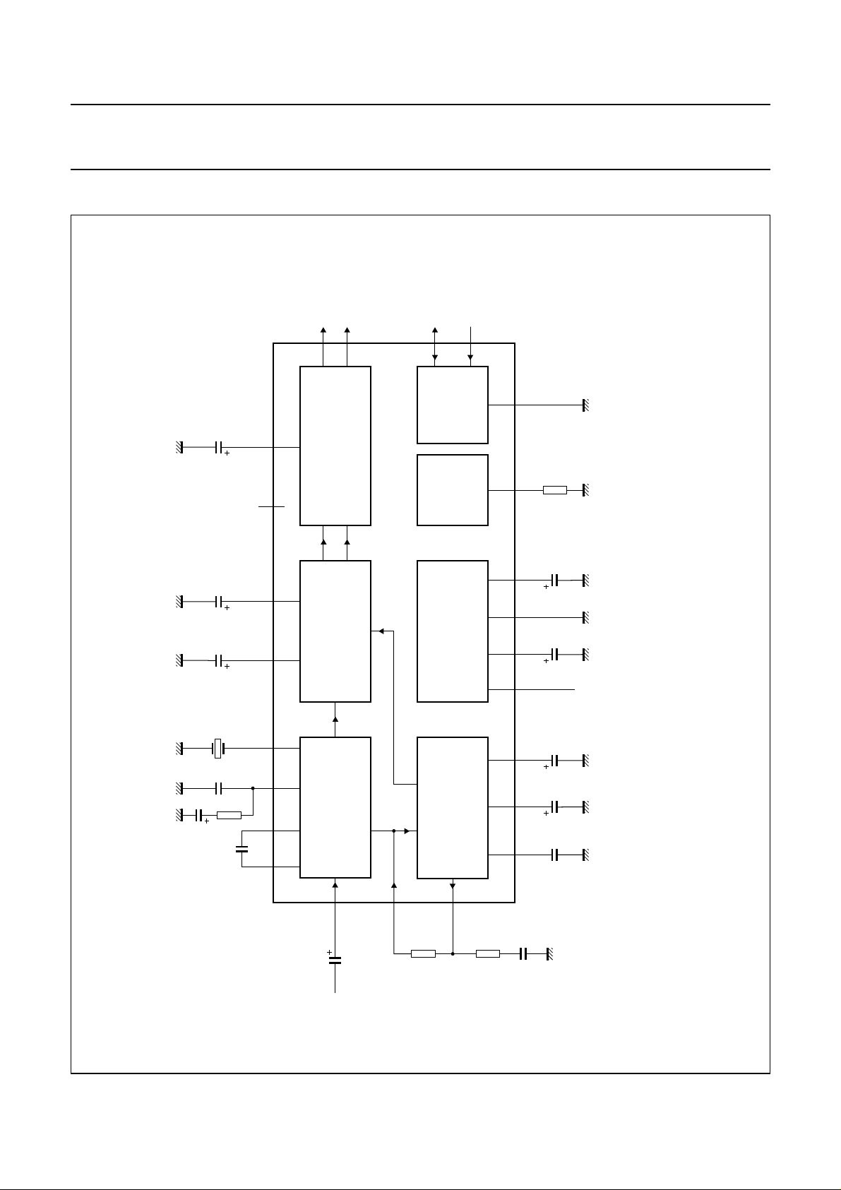
BLOCK DIAGRAM
OUTL
OUTR
12
13
n.c.
AV
1611
C
LEVEL
VOLUME
AUTOMATIC
C7
SDA
24
C-BUS
2
I
AND
FILTER
SCL
1
23
TRANSCEIVER
10
REFERENCE
DGND
FR
R
TDA9851
MHA969
R4
ook, full pagewidth
C3
C6
C5
Q1
C4
C2
R1
SS
C
MO
C
89
4
CER
PH
3
C
P2
6
C
P1
5
C
AND
DEMATRIX
MODE SELECT
L + R
STEREO DECODER
7COMP
C1
TDA9851
L − R
21FDI
SUPPLY
AND
VOLTAGE
DETECTOR
20FDO
R2
14
21522
AMPLIFIER
CONTROLLED
19 18 17
R3
ref
AGND V
CAP
V
TW
W
BPU C
C9
C15
C14
C10 C11 C13
V
CC
Fig.1 Block diagram.
composite
baseband
input
1997 Nov 12 3

Philips Semiconductors Product specification
I2C-bus controlled economic BTSC stereo
decoder
Component list
Electrolytic capacitors ±20%; foil capacitors ±10%; resistors ±5%; unless otherwise specified; see Fig.1.
COMPONENT VALUE TYPE REMARK
C1 2.2 µF electrolytic 63 V
C2 220 nF foil
C3 2.2 µF electrolytic 63 V
C4 220 nF foil
C5 2.2 µF electrolytic 63 V
C6 2.2 µF electrolytic 63 V
C7 4.7 µF electrolytic 63 V ±10%
C9 22 nF foil
C10 4.7 nF foil
C11 1 µF electrolytic 63 V
C13 10 µF electrolytic 63 V
C14 100 µF electrolytic 16 V
C15 100 µF electrolytic 16 V
R1 3.3 kΩ
R2 15 kΩ
R3 1.3 kΩ
R4 100 kΩ
Q1 CSB503F58 radial leads
CSB503JF958 alternative as SMD
TDA9851
1997 Nov 12 4
Philips Semiconductors Product specification
I2C-bus controlled economic BTSC stereo
decoder
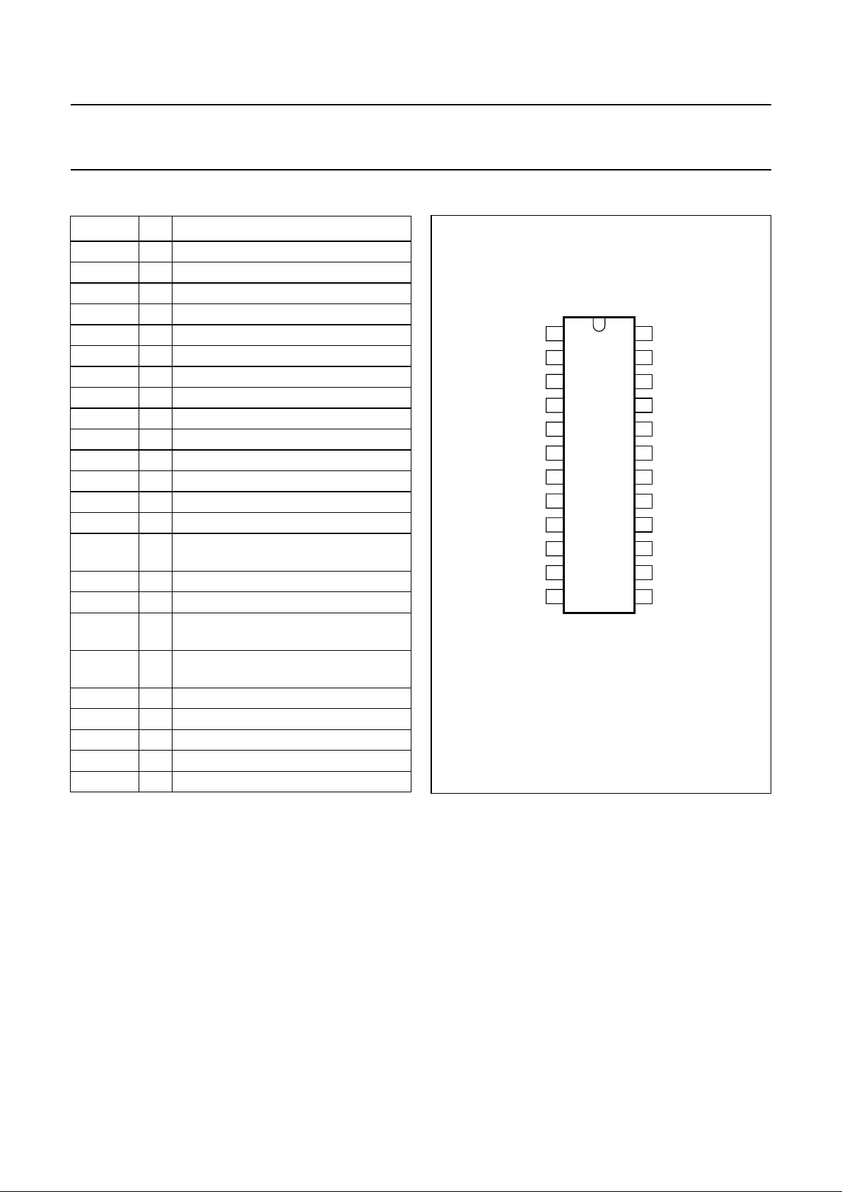
PINNING
SYMBOL PIN DESCRIPTION
2
SCL 1 serial clock input (I
V
CC
C
PH
2 supply voltage
3 capacitor for phase detector
CER 4 ceramic resonator
C
P1
C
P2
5 capacitor for pilot detector
6 capacitor for pilot detector
COMP 7 composite input signal
C
MO
C
SS
R
FR
8 capacitor DC-decoupling mono
9 capacitor DC-decoupling stereo
10 resistor for filter reference
n.c. 11 not connected
OUTL 12 output, left channel
OUTR 13 output, right channel
V
V
C
ref
CAP
AV
14 reference voltage 0.5V
capacitor for electronic filtering of
15
supply
16 automatic volume control capacitor
TW 17 capacitor timing
C
W
BPU
capacitor for VCA and band-pass filter
18
lower corner frequency
band-pass filter upper corner
19
frequency
FDO 20 fixed de-emphasis output
FDI 21 fixed de-emphasis input
AGND 22 analog ground
DGND 23 digital ground
SDA 24 serial data input/output (I
C-bus)
CC
2
C-bus)
handbook, halfpage
SCL
1
V
2
CC
C
3
PH
CER
4
C
5
P1
C
6
P2
COMP
C
MO
C
SS
R
FR
n.c.
OUTL
7
8
9
10
11
12
TDA9851
MHA968
Fig.2 Pin configuration.
TDA9851
SDA
24
DGND
23
AGND
22
FDI
21
FDO
20
19
BPU
C
18
W
TW
17
C
16
AV
V
15
CAP
V
14
ref
OUTR
13
1997 Nov 12 5
Philips Semiconductors Product specification
I2C-bus controlled economic BTSC stereo
decoder
FUNCTIONAL DESCRIPTION
Stereo decoder
The composite signal is fed into a pilot detector/pilot
cancellation circuit and into the MPX demodulator.
The main L + R signal passes a 75 µs fixed de-emphasis
filter and is fed into the dematrix circuit. The decoded
sub-signal L − R is sent to the VCA circuit. To generate the
pilot signal the stereo demodulator uses a PLL circuit
including a ceramic resonator.
Mode selection
The L − R signal is fed via the internal VCA circuit to the
dematrix/switching circuit. Mode selection is achieved via
2
C-bus.
the I
Automatic volume level control
The automatic volume level stage controls its output
voltage to a constant level of typically 200 mV (RMS) from
TDA9851
an input voltage range between 0.1 to 1.1 V (RMS).
The circuit adjusts variations in modulation during
broadcasting and because of changes in the programme
material. The function can be switched off. To avoid
audible plops during the permanent operation of the AVL
circuit a soft blending scheme has been applied between
the different gain stages. A capacitor (4.7 µF) at pin C
determines the attack and decay time constants.
In addition the ratio of attack and decay times can be
changed via the I2C-bus.
Integrated filters
The filter functions necessary for stereo demodulation are
provided on-chip using transconductor circuits. The filter
frequencies are controlled by the filter reference circuit via
the external resistor R4.
AV
LIMITING VALUES
In accordance with the Absolute Maximum Rating System (IEC 134).
SYMBOL PARAMETER CONDITIONS MIN. MAX. UNIT
V
CC
V
, V
SDA
SCL
V
n
T
amb
T
stg
V
es
supply voltage 0 9.9 V
voltage of SDA and SCL to GND VCC<9V 0 V
≥ 9V09V
V
CC
voltage of all other pins to GND 0 V
CC
CC
operating ambient temperature Tj< 125 °C −20 +70 °C
storage temperature −65 +150 °C
electrostatic handling note 1 −−V
Note
1. Machine model class B.
THERMAL CHARACTERISTICS
SYMBOL PARAMETER CONDITIONS VALUE UNIT
R
th(j-a)
thermal resistance from junction to ambient in free air
TDA9851 (SOT234-1; SDIP24) 55 K/W
TDA9851T (SOT137-1; SO24) 90 K/W
V
V
1997 Nov 12 6
 Loading...