

Philips tda9850 DATASHEETS

INTEGRATED CIRCUITS
DATA SH EET
TDA9850
2
I
C-bus controlled BTSC
stereo/SAP decoder
Preliminary specification
File under Integrated Circuits, IC02
1995 Jun 19
Philips Semiconductors Preliminary specification
I2C-bus controlled BTSC stereo/SAP decoder
FEATURES
• Quasi alignment-free application due to automatic
adjustment of channel separation via I2C-bus
• Dbx noise reduction circuit
• Dbx decoded stereo, Second Audio Program (SAP) or
mono selectable at the AF outputs
• Additional SAP output without dbx, including
de-emphasis
• High integration level with automatically tuned
integrated filters
2
• Input level adjustment I
C-bus controlled
• Alignment-free SAP processing
• Stereo pilot PLL circuit with ceramic resonator,
automatic adjustment procedure for stereo channel
separation, two pilot thresholds selectable via I2C-bus
• Automatic pilot cancellation
• Composite input noise detector with I2C-bus selectable
thresholds for stereo and SAP off
• I2C-bus transceiver.
GENERAL DESCRIPTION
The TDA9850 is a bipolar-integrated BTSC stereo/SAP
decoder (I
VCRs and multimedia.
TDA9850
2
C-bus controlled) for application in TV sets,
QUICK REFERENCE DATA
SYMBOL PARAMETER CONDITIONS MIN. TYP. MAX. UNIT
V
CC
I
CC
V
comp(rms)
V
oR(rms)
V
oL(rms)
G
LA
α
cs
THD
supply voltage 8.5 9 9.5 V
supply current − 58 75 mA
input signal voltage (RMS value) 100% modulation L + R; fi= 300 Hz − 250 − mV
;
output signal voltage (RMS value) 100% modulation L + R; fi= 300 Hz − 500 − mV
input level adjustment control −3.5 − +4.0 dB
stereo channel separation fL= 300 Hz; fR= 3 kHz 25 35 − dB
total harmonic distortion L + R fi= 1 kHz − 0.2 − %
L,R
S/N signal-to-noise ratio 500 mV (RMS) mono output signal
CCIR noise weighting filter
− 60 − dB
(peak value)
DIN noise weighting filter
− 73 − dBA
(RMS value)
ORDERING INFORMATION
PACKAGE
TYPE NUMBER
NAME DESCRIPTION VERSION
TDA9850 SDIP32 plastic shrink dual in-line package; 32 leads (400 mil) SOT232-1
TDA9850T SO32 plastic small outline package; 32 leads; body width 7.5 mm SOT287-1
1995 Jun 19 2

Philips Semiconductors Preliminary specification
I2C-bus controlled BTSC stereo/SAP decoder
License information
A license is required for the use of this product. For further information, please contact:
COMPANY BRANCH ADDRESS
THAT Corporation Licensing Operations 734 Forest St.
Marlborough, MA 01752
USA
Tel.: (508) 229-2500
Fax: (508) 229-2590
Tokyo Office 405 Palm House, 1-20-2 Honmachi
Shibuya-ku, Tokyo 151
Japan
Tel.: (03) 3378-0915
Fax: (03) 3374-5191
TDA9850
1995 Jun 19 3
Philips Semiconductors Preliminary specification
I2C-bus controlled BTSC stereo/SAP decoder
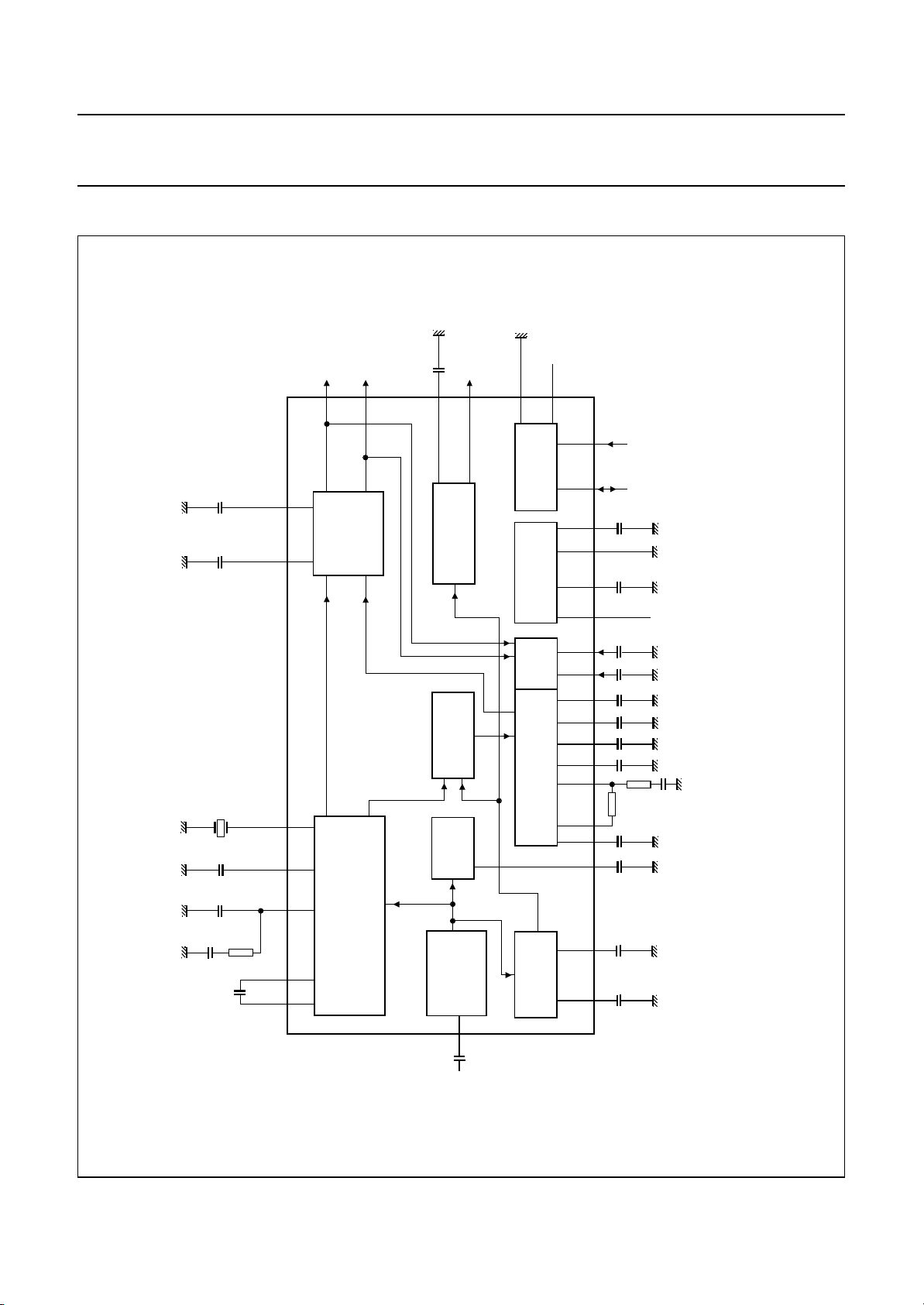
BLOCK DIAGRAM
stereo
mono
SAP
to
audio
processing
OUTL
ok, full pagewidth
+
C7
+
C6
ceramic
resonator
Q1
C5
+
C4
+
C3
C2
R1
OUTR
27
21
19
+
MODE
DEMATRIX
SELECT
L−R/SAP
18
L+R
TDA9850
17
16
15
STEREO DECODER
14
13
C8
22
DE-EMPHASIS
STEREO/SAP
NOISE
INPUT
11
+
SAP without DBX
23
SWITCH
DETECTOR
LEVEL
ADJUST
C1
7
C-
2
LOGIC, I
TRANSCEIVER
SUPPLY
ADJUST
STEREO
DBX
SAP
DEMODULATOR
28
MAD
MHA010
98
24
6
12
10
20
25
29
30
31
32
2
1
3
26
4
5
R2
TDA9850
SDA SCL
C18
+
C19
+
+
+
+
+
+
+
+
C17
C15
C16
+
R
C
L
C
C9
C10
C11
C12
C14
R3
ref
V
CAP
V
CC
V
only during
adjustment
C13
Fig.1 Block, application and test diagram.
1995 Jun 19 4
composite
baseband
input

Philips Semiconductors Preliminary specification
I2C-bus controlled BTSC stereo/SAP decoder
COMPONENT LIST
Electrolytic capacitors ±20%; foil capacitors ±10%; resistors ±5%; unless otherwise specified; see Fig.1.
COMPONENT VALUE TYPE REMARK
C1 10 µF electrolytic 63 V
C2 470 nF foil
C3 4.7 µF electrolytic 63 V
C4 220 nF foil
C5 10 µF electrolytic 63 V; I
C6 4.7 µF electrolytic 63 V
C7 4.7 µF electrolytic 63 V
C8 15 nF foil
C9 10 µF electrolytic 63 V ±10%
C10 10 µF electrolytic 63 V ±10%
C11 1 µF electrolytic 63 V
C12 1 µF electrolytic 63 V
C13 47 nF foil ±5%
C14 10 µF electrolytic 63 V
C15 100 nF foil
C16 4.7 µF electrolytic 63 V
C17 100 nF foil
C18 100 µF electrolytic 16 V
C19 100 µF electrolytic 16 V
CR 2.2 µF electrolytic 63 V
CL 2.2 µF electrolytic 63 V
R1 2.2 kΩ
R2 8.2 kΩ±2%
R3 160 Ω±2%
Q1 CSB503F58 radial leads
CSB503JF958 alternative as SMD
leak
< 1.5 µA
TDA9850
1995 Jun 19 5
Philips Semiconductors Preliminary specification
I2C-bus controlled BTSC stereo/SAP decoder
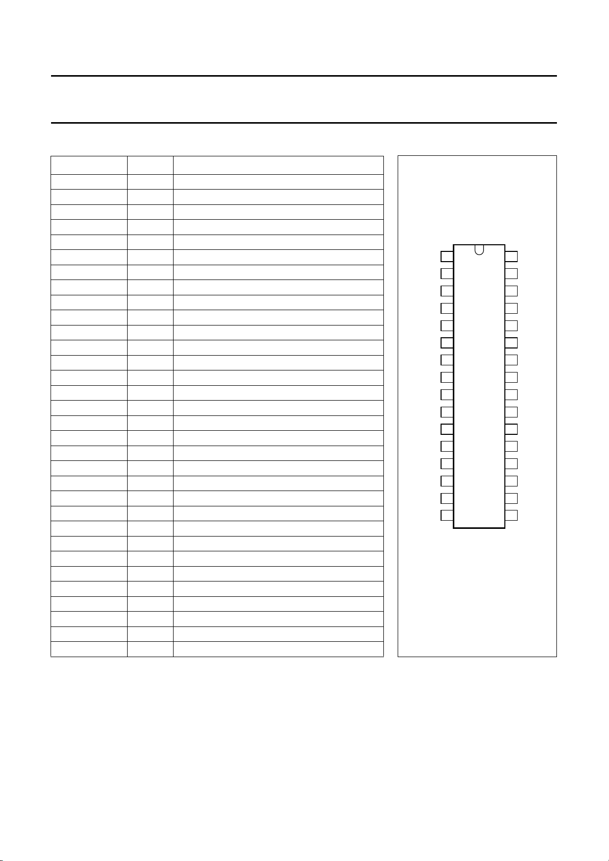
PINNING
SYMBOL PIN DESCRIPTION
VEO 1 variable emphasis output for dbx
VEI 2 variable emphasis input for dbx
C
NR
C
M
C
DEC
AGND 6 analog ground
DGND 7 digital ground
SDA 8 serial data input/output
SCL 9 serial clock input
V
CC
COMP 11 composite input signal
V
CAP
C
P1
C
P2
C
PH
C
ADJ
CER 17 ceramic resonator
C
MO
C
SS
C
R
OUTR 21 output, right channel
C
SDE
SAP 23 SAP output
V
ref
C
L
C
ND
OUTL 27 output, left channel
MAD 28 programmable address bit
C
TW
C
TS
C
W
C
S
3 capacitor noise reduction for dbx
4 capacitor mute for SAP
5 capacitor DC-decoupling for SAP
10 supply voltage (+9 V)
12 capacitor for electronic filtering of supply
13 capacitor for pilot detector
14 capacitor for pilot detector
15 capacitor for phase detector
16 capacitor for filter adjustment
18 capacitor DC-decoupling mono
19 capacitor DC-decoupling stereo/SAP
20 adjustment capacitor, right channel
22 capacitor SAP de-emphasis
24 reference voltage 0.5 × (VCC− 1.5 V)
25 adjustment capacitor, left channel
26 noise detector capacitor
29 capacitor timing wideband for dbx
30 capacitor timing spectral for dbx
31 capacitor wideband for dbx
32 capacitor spectral for dbx
TDA9850
page
1
VEO
2
VEI
C
3
NR
C
4
M
C
5
DEC
AGND OUTL
6
7
DGND
8
SDA
SCL
V
CC
COMP
V
CAP
C
P1
C
P2
C
PH
C
ADJ
9
10
11
12
13
14
15
16
TDA9850
MHA012
Fig.2 Pin configuration.
C
32
S
C
31
W
C
30
TS
C
29
TW
MAD
28
27
C
26
ND
C
25
L
V
24
ref
SAP
23
C
22
SDE
OUTR
21
C
20
R
C
19
SS
C
18
MO
CER
17
1995 Jun 19 6

Philips Semiconductors Preliminary specification
I2C-bus controlled BTSC stereo/SAP decoder
FUNCTIONAL DESCRIPTION
Input level adjustment
The composite input signal is fed to the input level
adjustment stage. The control range is from
−3.5 to +4.0 dB in steps of 0.5 dB. The subaddress
control 4 of Tables 5 and 6 and the level adjust setting of
Table 10 allows an optimum signal adjustment during the
set alignment. The maximum input signal voltage is
2 V (RMS).
Stereo decoder
The output signal of the level adjustment stage is coupled
to a low-pass filter which suppresses the baseband noise
above 125 kHz. The composite signal is then fed into a
pilot detector/pilot cancellation circuit and into the MPX
demodulator. The main L + R signal passes a 75 µs fixed
de-emphasis filter and is fed into the dematrix circuit. The
decoded sub-signal L − R is sent to the stereo/SAP switch.
To generate the pilot signal the stereo demodulator uses a
PLL circuit including a ceramic resonator. The stereo
channel separation is adjusted by an automatic procedure
to be performed during set production. For a detailed
description see Section “Adjustment procedure”. The
stereo identification can be read by the I
(see Table 2). Two different pilot thresholds (data
STS = 1; STS = 0) can be selected via the I2C-bus
(see Table 14).
SAP demodulator
2
C-bus
Noise detector
The composite input noise increases with decreasing
antenna signal. This makes it necessary to switch stereo
or SAP off at certain thresholds. These thresholds can be
set via the I
stereo threshold can be selected and with SP0 to SP3 the
SAP threshold. A hysteresis can be achieved via software
by making the threshold dependent of the identification
bits STP and SAPP (see Table 2).
Mode selection
The stereo/SAP switch feeds either the L − R signal or the
SAP demodulator output signal via the internal dbx noise
reduction circuit to the dematrix/switching circuit. Table 8
shows the different switch modes provided at the output
pins OUTR and OUTL.
dbx decoder
The dbx circuit includes all blocks required for the noise
reduction system in accordance with the BTSC system
specification. The output signal is fed through a 73 µs fixed
de-emphasis circuit to the dematrix block.
SAP output
Independent of the stereo/SAP switch, the SAP signal is
also available at pin SAP. At SAP, the SAP signal is not
dbx decoded. The capacitor at SDE provides a
recommended de-emphasis (150 µs) at SAP.
TDA9850
2
C-bus. With ST0 to ST3 (see Table 6) the
The composite signal is fed from the output of the input
level adjustment stage to the SAP demodulator circuit
through a 5f
automatically controlled. The SAP demodulator includes
an internal field strength detector that mutes the SAP
output in the event of insufficient signal conditions. The
SAP identification signal can be read by the I2C-bus
(see Table 2).
1995 Jun 19 7
band-pass filter. The demodulator level is
H
Integrated filters
The filter functions necessary for stereo and SAP
demodulation and part of the dbx filter circuits are provided
on-chip using transconductor circuits. The required filter
accuracy is attained by an automatic filter alignment
circuit.

Philips Semiconductors Preliminary specification
I2C-bus controlled BTSC stereo/SAP decoder
Adjustment procedure
C
OMPOSITE INPUT LEVEL ADJUSTMENT
Feed in from FM demodulator the composite signal with
100% modulation (25 kHz deviation) L + R; fi= 300 Hz.
Set input level control via I2C-bus monitoring OUTL or
OUTR (500 mV ±20 mV). Store the setting in a
non-volatile memory.
A
UTOMATIC ADJUSTMENT PROCEDURE
• Connect 2.2 µF capacitors from ACR and ACL to
ground.
• Composite input signal L = 300 Hz, R = 3.1 kHz,
14% modulation for each channel.
• Mode selection setting bits: STEREO = 1, SAP = 0
(see Table 8).
• Start adjustment by transmission ADJ = 1 in register
ALI3. The decoder will align itself.
• After 1 second minimum stop alignment by transmitting
ADJ = 0 in register ALI3 read the alignment data by an
I2C-bus read operation from ALR1 and ALR2
(see Chapter “I2C-bus protocol”) and store it in a
non-volatile memory. The alignment procedure
overwrites the previous data stored in ALI1 and ALI2.
• The capacitors from ACR and ACL may be
disconnected after alignment.
M
ANUAL ADJUSTMENT
Manual adjustment is necessary when no dual tone
generator is available (e.g. for service).
• Spectral and wideband data have to be set to 10000
(middle position for adjustment range)
• Composite input L = 300 Hz; 14% modulation
• Adjust channel separation by varying wideband data
• Composite input L = 3 kHz; 14% modulation
• Adjust channel separation by varying spectral data
• Iterative spectral/wideband operation for optimum
adjustment
• Store data in non-volatile memory.
After every power-on, the alignment data and the input
level adjustment data must be loaded from the non-volatile
memory.
IMING CURRENT FOR RELEASE RATE
T
Due to possible internal and external spreading, the timing
current can be adjusted via I2C-bus, see Table 9, as
recommended by dbx.
TDA9850
1995 Jun 19 8
Philips Semiconductors Preliminary specification
I2C-bus controlled BTSC stereo/SAP decoder
TDA9850
LIMITING VALUES
In accordance with the Absolute Maximum Rating System (IEC 134).
SYMBOL PARAMETER CONDITIONS MIN. MAX. UNIT
V
V
V
V
V
V
T
T
V
CC
VCAP
VEO
SDA
SCL
n
amb
stg
es
supply voltage 0 10 V
voltage of V
voltage of VEO to GND 0
to GND 0 V
CAP
CC
1
⁄2V
CC
V
V
voltage of SDA to GND 0 8.5 V
voltage of SCL to GND 0 8.5 V
voltage of all other pins to GND VCC≥ 8.5 V 0 8.5 V
< 8.5 V 0 V
V
CC
CC
V
operating ambient temperature Tj< 125 °C −20 +70 °C
storage temperature −65 +150 °C
electrostatic handling HBM; note 1
Note
1. Human Body Model (HBM): C = 100 pF; R = 1.5 kΩ; V = 2 kV; charge device model: C = 200 pF; R = 0 Ω;
V = 300 V.
THERMAL CHARACTERISTICS
SYMBOL PARAMETER VALUE UNIT
R
th j-a
thermal resistance from junction to ambient in free air
SOT232-1 55 K/W
SOT287-1 68 K/W
1995 Jun 19 9
 Loading...